ICGOO在线商城 > 集成电路(IC) > 线性 - 放大器 - 仪表,运算放大器,缓冲器放大器 > AD585SQ
 Datasheet下载
- 型号: AD585SQ
- 制造商: Analog
- 库位|库存: xxxx|xxxx
- 要求:
| 数量阶梯 | 香港交货 | 国内含税 |
| +xxxx | $xxxx | ¥xxxx |
查看当月历史价格
查看今年历史价格
AD585SQ产品简介:
ICGOO电子元器件商城为您提供AD585SQ由Analog设计生产,在icgoo商城现货销售,并且可以通过原厂、代理商等渠道进行代购。 AD585SQ价格参考¥636.30-¥736.46。AnalogAD585SQ封装/规格:线性 - 放大器 - 仪表,运算放大器,缓冲器放大器, 采样和保持 放大器 1 电路 14-CERDIP。您可以下载AD585SQ参考资料、Datasheet数据手册功能说明书,资料中有AD585SQ 详细功能的应用电路图电压和使用方法及教程。
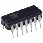
AD585SQ 是 Analog Devices Inc.(ADI)生产的一款高精度、低漂移的双极性运算放大器,属于线性放大器类别中的仪表、运算放大器及缓冲器放大器。该器件具有低输入偏置电流、低失调电压和高开环增益等特性,适用于对精度和稳定性要求较高的模拟信号处理场合。

AD585SQ 的典型应用场景包括:

1. 精密测量系统:如高精度传感器信号调理电路,用于温度、压力、重量等物理量的测量。
2. 工业控制设备:用于工业自动化系统中模拟信号的放大与处理,确保信号的高保真传输。
3. 医疗仪器:如心电图机、监护仪等设备中用于放大微弱生物电信号。
4. 测试与测量设备:如万用表、示波器前端信号处理电路,提供高精度和低噪声性能。
5. 音频设备:用于高端音频放大器中,提供低失真和高动态范围的音频信号放大。
6. 缓冲器与电压跟随器电路:利用其高输入阻抗和低输出阻抗特性,实现信号隔离与驱动。

AD585SQ 采用 8 引脚 SOIC 封装(SQ 后缀),适合在工业级温度范围内工作,具备良好的温度稳定性和长期可靠性,广泛应用于要求高性能模拟信号处理的场合。
| 参数 | 数值 |
| -3db带宽 | 2MHz |
| 产品目录 | 集成电路 (IC)半导体 |
| 描述 | IC OPAMP SAMPLE HOLD 2MHZ 14CDIP采样&保持放大器 IC HI SPD SAMPLE/ HOLD AMP |
| 产品分类 | Linear - Amplifiers - Instrumentation, OP Amps, Buffer Amps集成电路 - IC |
| 品牌 | Analog Devices |
| 产品手册 | |
| 产品图片 |
|
| rohs | 否不符合限制有害物质指令(RoHS)规范要求 |
| 产品系列 | 放大器 IC,采样&保持放大器,Analog Devices AD585SQ- |
| 数据手册 | |
| 产品型号 | AD585SQ |
| 产品 | Operational Amplifiers |
| 产品培训模块 | http://www.digikey.cn/PTM/IndividualPTM.page?site=cn&lang=zhs&ptm=30008http://www.digikey.cn/PTM/IndividualPTM.page?site=cn&lang=zhs&ptm=26202 |
| 产品种类 | 采样&保持放大器 |
| 供应商器件封装 | 14-CERDIP |
| 包装 | 管件 |
| 压摆率 | 10 V/µs |
| 商标 | Analog Devices |
| 增益带宽积 | - |
| 安装类型 | 通孔 |
| 安装风格 | Through Hole |
| 封装 | Tube |
| 封装/外壳 | 14-CDIP(0.300",7.62mm) |
| 封装/箱体 | CDIP-14 |
| 工作温度 | -55°C ~ 125°C |
| 工厂包装数量 | 25 |
| 捕获时间 | 3 us |
| 放大器类型 | 采样和保持 |
| 最大工作温度 | + 125 C |
| 最小双重电源电压 | - 10.8 V/5 V |
| 最小工作温度 | - 55 C |
| 标准包装 | 1 |
| 电压-电源,单/双 (±) | ±5 V ~ 18 V |
| 电压-输入失调 | 2mV |
| 电流-电源 | 10mA |
| 电流-输入偏置 | 2nA |
| 电流-输出/通道 | 50mA |
| 电源电压-最大 | 15 V |
| 电源电压-最小 | - 15 V |
| 电路数 | 1 |
| 系列 | AD585 |
| 视频文件 | http://www.digikey.cn/classic/video.aspx?PlayerID=1364138032001&width=640&height=505&videoID=2245193153001http://www.digikey.cn/classic/video.aspx?PlayerID=1364138032001&width=640&height=505&videoID=2245193159001 |
| 输出类型 | - |
| 通道数量 | 1 Channel |


- 商务部:美国ITC正式对集成电路等产品启动337调查
- 曝三星4nm工艺存在良率问题 高通将骁龙8 Gen1或转产台积电
- 太阳诱电将投资9.5亿元在常州建新厂生产MLCC 预计2023年完工
- 英特尔发布欧洲新工厂建设计划 深化IDM 2.0 战略
- 台积电先进制程称霸业界 有大客户加持明年业绩稳了
- 达到5530亿美元!SIA预计今年全球半导体销售额将创下新高
- 英特尔拟将自动驾驶子公司Mobileye上市 估值或超500亿美元
- 三星加码芯片和SET,合并消费电子和移动部门,撤换高东真等 CEO
- 三星电子宣布重大人事变动 还合并消费电子和移动部门
- 海关总署:前11个月进口集成电路产品价值2.52万亿元 增长14.8%


PDF Datasheet 数据手册内容提取
a High Speed, Precision Sample-and-Hold Amplifier AD585 FEATURES FUNCTIONAL BLOCK DIAGRAM 3.0 (cid:109)s Acquisition Time to (cid:54)0.01% max Low Droop Rate: 1.0 mV/ms max DIP LCC/PLCC Package Sample/Hold Offset Step: 3 mV max Aperture Jitter: 0.5 ns Extended Temperature Range: –55(cid:56)C to +125(cid:56)C Internal Hold Capacitor Internal Application Resistors (cid:54)12 V or (cid:54)15 V Operation Available in Surface Mount APPLICATIONS Data Acquisition Systems Data Distribution Systems Analog Delay & Storage Peak Amplitude Measurements MIL-STD-883 Compliant Versions Available The AD585 is available in three performance grades. The JP PRODUCT DESCRIPTION grade is specified for the 0(cid:176) C to +70(cid:176) C commercial temperature The AD585 is a complete monolithic sample-and-hold circuit range and packaged in a 20-pin PLCC. The AQ grade is speci- consisting of a high performance operational amplifier in series fied for the –25(cid:176) C to +85(cid:176) C industrial temperature range and is with an ultralow leakage analog switch and a FET input inte- packaged in a 14-pin cerdip. The SQ and SE grades are speci- grating amplifier. An internal holding capacitor and matched fied for the –55(cid:176) C to +125(cid:176) C military temperature range and applications resistors have been provided for high precision and are packaged in a 14-pin cerdip and 20-pin LCC. applications flexibility. The performance of the AD585 makes it ideal for high speed PRODUCT HIGHLIGHTS 10- and 12-bit data acquisition systems, where fast acquisition 1. The fast acquisition time (3 m s) and low aperture jitter time, low sample-to-hold offset, and low droop are critical. The (0.5 ns) make it the first choice for very high speed data AD585 can acquire a signal to – 0.01% in 3 m s maximum, and acquisition systems. then hold that signal with a maximum sample-to-hold offset of 2. The droop rate is only 1.0 mV/ms so that it may be used in 3 mV and less than 1 mV/ms droop, using the on-chip hold slower high accuracy systems without the loss of accuracy. capacitor. If lower droop is required, it is possible to add a larger external hold capacitor. 3. The low charge transfer of the analog switch keeps sample-to hold offset below 3 mV with the on-chip 100 pF hold capaci- The high speed analog switch used in the AD585 exhibits tor, eliminating the trade-off between acquisition time and aperture jitter of 0.5 ns, enabling the device to sample full scale S/H offset required with other SHAs. (20 V peak-to-peak) signals at frequencies up to 78 kHz with 12-bit precision. 4. The AD585 has internal pretrimmed application resistors for applications versatility. The AD585 can be used with any user-defined feedback net- work to provide any desired gain in the sample mode. On-chip 5. The AD585 is complete with an internal hold capacitor for precision thin-film resistors can be used to provide gains of +1, ease of use. Capacitance can be added externally to reduce –1, or +2. Output impedance in the hold mode is sufficiently the droop rate when long hold times and high accuracy are low to maintain an accurate output signal even when driving the required. dynamic load presented by a successive-approximation A/D 6. The AD585 is recommended for use with 10- and 12-bit converter. However, the output is protected against damage successive-approximation A/D converters such as AD573, from accidental short circuits. AD574A, AD674A, AD7572 and AD7672. The control signal for the HOLD command can be either active 7. The AD585 is available in versions compliant with MIL-STD- high or active low. The differential HOLD signal is compatible 883. Refer to the Analog Devices Military Products Databook with all logic families, if a suitable reference level is provided. An or current AD585/883B data sheet for detailed specifications. on-chip TTL reference level is provided for TTL compatibility. REV.A Information furnished by Analog Devices is believed to be accurate and reliable. However, no responsibility is assumed by Analog Devices for its use, nor for any infringements of patents or other rights of third parties which may result from its use. No license is granted by implication or One Technology Way, P.O. Box 9106, Norwood, MA 02062-9106, U.S.A. otherwise under any patent or patent rights of Analog Devices. Tel: 617/329-4700 Fax: 617/326-8703
AD585–SPECIFICATIONS(typical @ +25(cid:56)C and V = (cid:54)12 V or (cid:54)15 V, and C = Internal, A = +1, S H HOLD active unless otherwise noted) Model AD585J AD585A AD585S Min Typ Max Min Typ Max Min Typ Max Units SAMPLE/HOLD CHARACTERISTICS Acquisition Time, 10 V Step to 0.01% 3 3 3 m s 20 V Step to 0.01% 5 5 5 m s Aperture Time, 20 V p-p Input, HOLD 0 V 35 35 35 ns Aperture Jitter, 20 V p-p Input, HOLD 0 V 0.5 0.5 0.5 ns Settling Time, 20 V p-p Input, HOLD 0 V, to 0.01% 0.5 0.5 0.5 m s Droop Rate 1 1 1 mV/ms Droop Rate T to T Doubles Every 10(cid:176)C Double Every 10(cid:176)C Doubles Every 10(cid:176)C MIN MAX Charge Transfer 0.3 0.3 0.3 pC Sample-to-Hold Offset –3 3 –3 3 –3 3 mV Feedthrough 20 V p-p, 10 kHz Input 0.5 0.5 0.5 mV TRANSFER CHARACTERISTICS1 Open Loop Gain V = 20 V p-p, R = 2k 200,000 200,000 200,000 V/V OUT L Application Resistor Mismatch 0.3 0.3 0.3 % Common-Mode Rejection V = – 10 V 80 80 80 dB CM Small Signal Gain Bandwidth V = 100 mV p-p 2.0 2.0 2.0 MHz OUT Full Power Bandwidth V = 20 V p-p 160 160 160 kHz OUT Slew Rate V = 20 V p-p 10 10 10 V/m s OUT Output Resistance (Sample Mode) I = – 10 mA 0.05 0.05 0.05 W OUT Output Short Circuit Current 50 50 50 mA Output Short Circuit Duration Indefinite Indefinite Indefinite ANALOG INPUT CHARACTERISTICS Offset Voltage 5 2 2 mV Offset Voltage, T to T 6 3 3 mV MIN MAX Bias Current 2 2 2 nA Bias Current, T to T 5 5 20 502 nA MIN MAX Input Capacitance, f = 1 MHz 10 10 10 pF Input Resistance, Sample or Hold 20 V p-p Input, A = +1 1012 1012 1012 W DIGITAL INPUT CHARACTERISTICS TTL Reference Output 1.2 1.4 1.6 1.2 1.4 1.6 1.2 1.4 1.6 V Logic Input High Voltage T to T 2.0 2.0 2.0 V MIN MAX Logic Input Low Voltage T to T 0.8 0.8 0.7 V MIN MAX Logic Input Current (Either Input) 50 50 50 m A POWER SUPPLY CHARACTERISTICS Operating Voltage Range +5, –10.8 – 18 +5, –10.8 – 18 +5, –10.8 – 18 V Supply Current, R = ¥ 6 10 6 10 6 10 mA L Power Supply Rejection, Sample Mode 70 70 70 dB TEMPERATURE RANGE Specified Performance 0 +70 –25 +85 –55 +125 (cid:176)C PACKAGE OPTIONS3, 4 Cerdip (Q-14) AD585AQ AD585SQ LCC (E-20A) AD585SE PLCC (P-20A) AD585JP NOTES Specifications subject to change without notice. 1Maximum input signal is the minimum supply minus a headroom voltage of 2.5 V. 2Not tested at –55(cid:176)C. Specifications shown in boldface are tested on all production units at final electrical 3E = Leadless Ceramic Chip Carrier; P = Plastic Leaded Chip Carrier; Q = Cerdip. test. Results from those tests are used to calculate outgoing quality levels. 4For AD585/883B specifications, refer to Analog Devices Military Products Databook. All min and max specifications are guaranteed, although only those shown in boldface are tested on all production units. –2– REV. A
AD585 ABSOLUTE MAXIMUM RATINGS Supplies (+V , –V ) . . . . . . . . . . . . . . . . . . . . . . . . . . . . .– 18 V S S Logic Inputs . . . . . . . . . . . . . . . . . . . . . . . . . . . . . . . . . . . – V S Analog Inputs . . . . . . . . . . . . . . . . . . . . . . . . . . . . . . . . . . – V S R , R Pins . . . . . . . . . . . . . . . . . . . . . . . . . . . . . . . . . . . – V IN FB S Storage Temperature . . . . . . . . . . . . . . . . . . .–65(cid:176) C to +150(cid:176) C Lead Temperature (Soldering) . . . . . . . . . . . . . . . . . . . 300(cid:176) C Output Short Circuit to Ground . . . . . . . . . . . . . . . .Indefinite TTL Logic Reference Short Circuit to Ground . . . . . . . . . . . . . . . . . . . . . . . . .Indefinite Figure 2.Acquisition Time vs. Hold Capacitance (10 V Step to 0.01%) REV. A –3–
AD585 SAMPLED DATA SYSTEMS (cid:177)(cid:40)(cid:78) +(cid:49)(cid:41) (cid:50) In sampled data systems there are a number of limiting factors (cid:102) = in digitizing high frequency signals accurately. Figure 9 shows (cid:77)(cid:65)(cid:88) p (cid:40)(cid:65)(cid:112)(cid:101)(cid:114)(cid:116)(cid:117)(cid:114)(cid:101) (cid:74)(cid:105)(cid:116)(cid:116)(cid:101)(cid:114)(cid:41) pictorially the sample-and-hold errors that are the limiting fac- tors. In the following discussions of error sources the errors will For an application with a 10-bit A/D converter with a 10 V full be divided into the following groups: 1. Sample-to-Hold Transi- scale to a 1/2 LSB error maximum. tion, 2. Hold Mode and 3. Hold-to-Sample Transition. (cid:177)(cid:40)(cid:49)(cid:48)+(cid:49)(cid:41) (cid:50) (cid:102) = (cid:77)(cid:65)(cid:88) p (cid:40)(cid:48)(cid:46)(cid:53)· (cid:49)(cid:48)(cid:177)(cid:57)(cid:41) (cid:102) =(cid:51)(cid:49)(cid:48)(cid:46)(cid:56)(cid:107)(cid:72)(cid:122)(cid:46) (cid:77)(cid:65)(cid:88) For an application with a 12-bit A/D converter with a 10 V full scale to a 1/2 LSB error maximum: (cid:177)(cid:40)(cid:49)(cid:50)+(cid:49)(cid:41) (cid:50) (cid:102) = (cid:77)(cid:65)(cid:88) p (cid:40)(cid:48)(cid:46)(cid:53)· (cid:49)(cid:48)(cid:177)(cid:57)(cid:41) (cid:102) =(cid:55)(cid:55)(cid:46)(cid:55)(cid:107)(cid:72)(cid:122)(cid:46) (cid:77)(cid:65)(cid:88) Figure 11 shows the entire range of errors induced by aperture Figure 9.Pictorial Showing Various S/H Characteristics jitter with respect to the input signal frequency. SAMPLE-TO-HOLD TRANSITION The aperture delay time is the time required for the sample-and- hold amplifier to switch from sample to hold. Since this is effec- tively a constant then it may be tuned out. If however, the aperture delay time is not accounted for then errors of the mag- nitude as shown in Figure 10 will result. Figure 11.Aperture Jitter Error vs. Frequency Sample-to-hold offset is caused by the transfer of charge to the holding capacitor via the gate capacitance of the switch when switching into hold. Since the gate capacitance couples the switch control voltage applied to the gate on to the hold capaci- tor, the resulting sample-to-hold offset is a function of the logic level . Figure 10.Aperture Delay Error vs. Frequency The logic inputs were designed for application flexibility and, To eliminate the aperture delay as an error source the sample- therefore, a wide range of logic thresholds. This was achieved by to-hold command may be advanced with respect to the input using a differential input stage for HOLD and HOLD. Figure 1 signal . shows the change in the sample-to-hold offset voltage based Once the aperture delay time has been eliminated as an error upon an independently programmed reference voltage. Since source then the aperture jitter which is the variation in aperture the input stage is a differential configuration, the offset voltage delay time from sample-to-sample remains. The aperture jitter is is a function of the control voltage range around the pro- a true error source and must be considered. The aperture jitter grammed threshold voltage. is a result of noise within the switching network which modu- The sample-to-hold offset can be reduced by adding capacitance lates the phase of the hold command and is manifested in the to the internal 100 pF capacitor and by using HOLD instead of variations in the value of the analog input that has been held. HOLD. This may be easily accomplished by adding an external The aperture error which results from this jitter is directly re- capacitor between Pins 7 and 8. The sample-to-hold offset is lated to the dV/dT of the analog input. then governed by the relationship: The error due to aperture jitter is easily calculated as shown be- ( ) (cid:67)(cid:104)(cid:97)(cid:114)(cid:103)(cid:101) (cid:112)(cid:67) low. The error calculation takes into account the desired accu- (cid:83)(cid:47)(cid:72) (cid:79)(cid:102)(cid:102)(cid:115)(cid:101)(cid:116)(cid:40)(cid:86)(cid:41)= racy corresponding to the resolution of the N-bit A/D converter. (cid:67)(cid:72) (cid:84)(cid:111)(cid:116)(cid:97)(cid:108)(cid:40)(cid:112)(cid:70)(cid:41) –4– REV. A
AD585 For the AD585 in particular it becomes: HOLD-TO-SAMPLE TRANSITION The Nyquist theorem states that a band-limited signal which is (cid:48)(cid:46)(cid:51)(cid:32)(cid:112)(cid:67) (cid:83)(cid:47)(cid:72) (cid:79)(cid:102)(cid:102)(cid:115)(cid:101)(cid:116)(cid:40)(cid:86)(cid:41)=(cid:49)(cid:48)(cid:48) (cid:112)(cid:70) +((cid:67) ) scaamn pblee dre acto na srtartuec taetd l ewasitth towuitc elo tshse o mf ianxfiomrmumat isoingn. aTl hfrise qmueeanncsy (cid:69)(cid:88)(cid:84) that a sampled data system must sample, convert and acquire The addition of an external hold capacitor also affects the acqui- the next point at a rate at least twice the signal frequency. Thus sition time of the AD585. The change in acquisition time with the maximum input frequency is equal to respect to the C is shown graphically in Figure 2. EXT (cid:49) (cid:102) = HOLD MODE (cid:77)(cid:65)(cid:88) (cid:50)((cid:84) +(cid:84) +(cid:84) ) In the hold mode there are two important specifications that (cid:65)(cid:67)(cid:81) (cid:67)(cid:79)(cid:78)(cid:86) (cid:65)(cid:80) must be considered; feedthrough and the droop rate. Feedthrough Where T is the acquisition time of the sample-to-hold ACQ errors appear as an attenuated version of the input at the output amplifier, T is the maximum aperture time (small enough to AP while in the hold mode. Hold-Mode feedthrough varies with fre- be ignored) and T is the conversion time of the A/D CONV quency, increasing at higher frequencies. Feedthrough is an im- converter. portant specification when a sample and hold follows an analog multiplexer that switches among many different channels. DATA ACQUISITION SYSTEMS Hold-mode droop rate is the change in output voltage per unit The fast acquisition time of the AD585 when used with a high of time while in the hold mode. Hold-mode droop originates as speed A/D converter allows accurate digitization of high fre- leakage from the hold capacitor, of which the major leakage quency signals and high throughput rates in multichannel data current contributors are switch leakage current and bias current. acquisition systems. The AD585 can be used with a number of The rate of voltage change on the capacitor dV/dT is the ratio of different A/D converters to achieve high throughput rates. Fig- the total leakage current I to the hold capacitance C . ures 12 and 13 show the use of an AD585 with the AD578 and L H AD574A. (cid:100)(cid:86) (cid:73) (cid:40)(cid:112)(cid:65)(cid:41) (cid:68)(cid:114)(cid:111)(cid:111)(cid:112) (cid:82)(cid:97)(cid:116)(cid:101)= (cid:79)(cid:85)(cid:84) (cid:40)(cid:86)(cid:111)(cid:108)(cid:116)(cid:115)(cid:47)(cid:83)(cid:101)(cid:99)(cid:41) = (cid:76) (cid:100)(cid:84) (cid:67) (cid:40)(cid:112)(cid:70)(cid:41) (cid:72) For the AD585 in particular; (cid:49)(cid:48)(cid:48) (cid:112)(cid:65) (cid:68)(cid:114)(cid:111)(cid:111)(cid:112) (cid:82)(cid:97)(cid:116)(cid:101) = (cid:49)(cid:48)(cid:48) (cid:112)(cid:70) +(cid:40)(cid:67) (cid:41) (cid:69)(cid:88)(cid:84) Additionally the leakage current doubles for every 10(cid:176) C increase in temperature above 25(cid:176) C; therefore, the hold-mode droop rate characteristic will also double in the same fashion. The hold-mode droop rate can be traded-off with acquisition time to provide the best combination of droop error and acquisition time. The tradeoff is easily accomplished by varying the value of C . EXT Since a sample and hold is used typically in combination with Figure 12.A/D Conversion System, 117.6 kHz Throughput an A/D converter, then the total droop in the output voltage has 58.8 kHz max Signal Input to be less than 1/2 LSB during the period of a conversion. The maximum allowable signal change on the input of an A/D converter is: (cid:70)(cid:117)(cid:108)(cid:108)(cid:45)(cid:83)(cid:99)(cid:97)(cid:108)(cid:101)(cid:32)(cid:86)(cid:111)(cid:108)(cid:116)(cid:97)(cid:103)(cid:101) D (cid:86) (cid:109)(cid:97)(cid:120)(cid:61) ((cid:78)+(cid:49)) (cid:50) Once the maximum D V is determined then the conversion time of the A/D converter (T ) is required to calculate the maxi- CONV mum allowable dV/dT. (cid:100)(cid:86) D (cid:86)(cid:109)(cid:97)(cid:120) (cid:109)(cid:97)(cid:120) = (cid:100)(cid:116) (cid:84) (cid:67)(cid:79)(cid:78)(cid:86) (cid:100)(cid:86) (cid:109)(cid:97)(cid:120) The maximum as shown by the previous equation is (cid:100)(cid:84) the limit not only at 25(cid:176) C but at the maximum expected operat- ing temperature range. Therefore, over the operating temperature Figure 13.12-Bit A/D Conversion System, 26.3 kHz range the following criteria must be met (T –25(cid:176) C) OPERATION Throughput Rate, 13.1 kHz max Signal Input = D T. (D (cid:84)(cid:176)(cid:67)) (cid:100)(cid:86) (cid:50)(cid:53)(cid:176) (cid:67) · (cid:50) (cid:49)(cid:48)(cid:176)(cid:67) £ (cid:100)(cid:86) (cid:109)(cid:97)(cid:120) (cid:100)(cid:84) (cid:100)(cid:84) REV. A –5–
AD585 LOGIC INPUT ence between the voltage being measured and the voltage previ- The sample-and-hold logic control was designed for versatile ously measured determines the fraction by which the logic interfacing. The HOLD and HOLD inputs may be used dielectric absorption figure is multiplied. It is impossible to with both low and high level CMOS, TTL and ECL logic sys- readily correct for this error source. The only solution is to use a tems. Logic threshold programmability was achieved by using a capacitor with dielectric absorption less than the maximum differential amplifier as the input stage for the digital inputs. A tolerable error. Capacitor types such as polystyrene, polypropy- predictable logic threshold may be programmed by referencing lene or Teflon are recommended. 9 either HOLD or HOLD to the appropriate threshold voltage. 8 4/ For example, if the internal 1.4 V reference is applied to HOLD GROUNDING 5– – an input signal to HOLD between +1.8 V and +V will place Many data-acquisition components have two or more ground c S 1 the AD585 in the hold mode. The AD585 will go into the pins which are not connected together within the device. These 85 C sample mode for this case when the input is between –V and “grounds” are usually referred to as the Logic Power Return S +1.0 V. The range of references which may be applied is from Analog Common (Analog Power Return), and Analog Signal (–V +4 V) to (+V –3 V). Ground. These grounds must be tied together at one point, S S usually at the system power-supply ground. Ideally, a single OPTIONAL CAPACITOR SELECTION solid ground would be desirable. However, since current flows If an additional capacitor is going to be used in conjunction through the ground wires and etch stripes of the circuit cards, with the internal 100 pF capacitor it must have a low dielectric and since these paths have resistance and inductance, hundreds absorption. Dielectric absorption is just that; it is the charge of millivolts can be generated between the system ground point absorbed into the dielectric that is not immediately added to or and the ground pin of the AD585. Separate ground returns removed from the capacitor when rapidly charged or discharged. should be provided to minimize the current flow in the path The capacitor with dielectric absorption is modeled in Figure 14. from sensitive points to the system ground point. In this way supply currents and logic-gate return currents are not summed into the same return path as analog signals where they would cause measurement errors. Figure 14.Capacitor Model with Dielectric Absorption If the capacitor is charged slowly, C will eventually charge to DA the same value as C. But unfortunately, good dielectrics have very high resistances, so while C may be small, R is large and DA X the time constant R C typically runs into the millisecond X DA range. In fast charge, fast-discharge situations the effect of di- electric absorption resembles “memory”. In a data acquisition system where many channels with widely varying data are being sampled the effect is to have an ever changing offset which ap- pears as a very nonlinear sample-to-hold offset since the differ- Figure 15.Basic Grounding Practice OUTLINE DIMENSIONS Dimensions shown in inches and (mm). 14-Pin Cerdip (Q-14) 20-Terminal LCC (E-20A) 20-Terminal PLCC (P-20A) A. S. U. N D I E T N RI P –6– REV. A