ICGOO在线商城 > 集成电路(IC) > PMIC - 电压基准 > AD580LH
 Datasheet下载
- 型号: AD580LH
- 制造商: Analog
- 库位|库存: xxxx|xxxx
- 要求:
| 数量阶梯 | 香港交货 | 国内含税 |
| +xxxx | $xxxx | ¥xxxx |
查看当月历史价格
查看今年历史价格
AD580LH产品简介:
ICGOO电子元器件商城为您提供AD580LH由Analog设计生产,在icgoo商城现货销售,并且可以通过原厂、代理商等渠道进行代购。 AD580LH价格参考。AnalogAD580LH封装/规格:PMIC - 电压基准, 系列 电压基准 IC ±0.4% 10mA TO-52-3。您可以下载AD580LH参考资料、Datasheet数据手册功能说明书,资料中有AD580LH 详细功能的应用电路图电压和使用方法及教程。
AD580LH是Analog Devices Inc.(现为亚德诺半导体,ADI)生产的一款高精度、低温漂电压基准芯片,属于PMIC(电源管理集成电路)中的电压基准类别。它广泛应用于需要高精度电压参考的场合,以下是其主要应用场景:

1. 精密测量仪器:AD580LH因其高精度和低温度系数特性,非常适合用于精密电压表、电流表、功率计等测量设备中,确保测量结果的准确性。

2. 数据采集系统:在数据采集系统中,AD580LH可以用作模数转换器(ADC)或数模转换器(DAC)的参考电压源,提供稳定可靠的基准电压,从而提高系统的整体精度和稳定性。

3. 自动测试设备(ATE):在自动化测试环境中,AD580LH可以为各种测试模块提供稳定的电压基准,确保测试结果的一致性和可靠性,特别是在对精度要求极高的半导体测试设备中。

4. 工业控制系统:在工业自动化领域,AD580LH可用于传感器信号调理电路中,作为电压基准源,帮助实现精确的信号放大和处理,适用于温度、压力、流量等物理量的精确测量和控制。

5. 医疗设备:在医疗电子设备中,如心电图机、血压计等,AD580LH可以提供高精度的电压基准,确保设备能够准确地检测和记录生理信号,保障诊断结果的可靠性。

6. 通信设备:在通信基站和终端设备中,AD580LH可以用作射频前端模块的电压基准,确保信号发射和接收的稳定性和精度,特别是在需要高动态范围和低噪声的应用中。

7. 航空航天与国防:在这些领域的高精度导航、雷达和卫星通信系统中,AD580LH的高可靠性和稳定性使其成为理想的选择,确保关键任务系统的性能和安全性。

总之,AD580LH凭借其卓越的性能和可靠性,在众多对电压基准有严格要求的应用场景中发挥着重要作用。
| 参数 | 数值 |
| 产品目录 | 集成电路 (IC)半导体 |
| 描述 | IC VREF SERIES PREC 2.5V TO-52-3参考电压 HI PREC 2.5V IC REF |
| 产品分类 | |
| 品牌 | Analog Devices |
| 产品手册 | |
| 产品图片 |
|
| rohs | 符合RoHS无铅 / 符合限制有害物质指令(RoHS)规范要求 |
| 产品系列 | 电源管理 IC,参考电压,Analog Devices AD580LH- |
| 数据手册 | |
| 产品型号 | AD580LH |
| 产品目录页面 | |
| 产品种类 | 参考电压 |
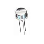
| 供应商器件封装 | TO-52-3 |
| 初始准确度 | 0.4 % |
| 包装 | 散装 |
| 参考类型 | Series Precision References |
| 商标 | Analog Devices |
| 安装类型 | 通孔 |
| 安装风格 | Through Hole |
| 容差 | ±0.4% |
| 封装 | Bulk |
| 封装/外壳 | TO-205AA,TO-5-3 金属罐 |
| 封装/箱体 | TO-52-3 |
| 工作温度 | 0°C ~ 70°C |
| 工厂包装数量 | 100 |
| 平均温度系数—典型值 | 25 PPM / C |
| 最大工作温度 | + 125 C |
| 最小工作温度 | - 55 C |
| 标准包装 | 1 |
| 温度系数 | 25ppm/°C |
| 电压-输入 | 4.5 V ~ 30 V |
| 电压-输出 | 2.5V |
| 电流-输出 | 10mA |
| 电流-阴极 | - |
| 电流-静态 | 1.5mA |
| 系列 | AD580 |
| 输出电压 | 2.5 V |
| 通道数 | 1 |


- 商务部:美国ITC正式对集成电路等产品启动337调查
- 曝三星4nm工艺存在良率问题 高通将骁龙8 Gen1或转产台积电
- 太阳诱电将投资9.5亿元在常州建新厂生产MLCC 预计2023年完工
- 英特尔发布欧洲新工厂建设计划 深化IDM 2.0 战略
- 台积电先进制程称霸业界 有大客户加持明年业绩稳了
- 达到5530亿美元!SIA预计今年全球半导体销售额将创下新高
- 英特尔拟将自动驾驶子公司Mobileye上市 估值或超500亿美元
- 三星加码芯片和SET,合并消费电子和移动部门,撤换高东真等 CEO
- 三星电子宣布重大人事变动 还合并消费电子和移动部门
- 海关总署:前11个月进口集成电路产品价值2.52万亿元 增长14.8%


PDF Datasheet 数据手册内容提取
High Precision, 2.5 V IC Reference AD580 FUNCTIONAL BLOCK DIAGRAM FEATURES Laser-trimmed to high accuracy: 2.500 V ±0.4% +E 3-terminal device: voltage in/voltage out Excellent temperature stability: 10 ppm/°C (AD580M, U) BOTTOM EOUT Excellent long-term stability: 250 μV (25 μV/month) VIEW Low quiescent current: 1.5 mA maximum SMmILa-lSl,T hDe-r8m83e tcioc mICp pliaacnkta vgeer:s TioOn-s5 2a vcaainla ble –E 00525-B-001 Figure 1. GENERAL DESCRIPTION PRODUCT HIGHLIGHTS 1. Laser-trimming of the thin film resistors minimizes the The AD580 is a 3-terminal, low cost, temperature-compensated, AD580 output error. For example, the AD580L output bandgap voltage reference, which provides a fixed 2.5 V output tolerance is ±10 mV. for inputs between 4.5 V and 30 V. A unique combination of 2. The three-terminal voltage in/voltage out operation of the advanced circuit design and laser-wafer trimmed thin film AD580 provides regulated output voltage without any resistors provide the AD580 with an initial tolerance of ±0.4%, a external components. temperature stability of better than 10 ppm/°C, and long-term 3. The AD580 provides a stable 2.5 V output voltage for input stability of better than 250 μV. In addition, the low quiescent voltages between 4.5 V and 30 V. The capability to provide current drain of 1.5 mA maximum offers a clear advantage over a stable output voltage using a 5 V input makes the AD580 classical Zener techniques. an ideal choice for systems that contain a single logic The AD580 is recommended as a stable reference for all 8-, 10-, power supply. and 12-bit D/A converters that require an external reference. In 4. Thin film resistor technology and tightly controlled bipolar addition, the wide input range of the AD580 allows operation processing provide the AD580 with temperature stabilities with 5 volt logic supplies, making the AD580 ideal for digital to 10 ppm/°C and long-term stability better than 250 μV. panel meter applications or whenever only a single logic power 5. The low quiescent current drain of the AD580 makes it supply is available. ideal for CMOS and other low power applications. 6. The AD580 is available in versions compliant with MIL- The AD580J, K, L, and M are specified for operation over the STD-883. Refer to the Analog Devices Military Products 0°C to +70°C temperature range; the AD580S, T, and U are Data Book or the current AD580/AD883B data sheet for specified for operation over the extended temperature range of detailed specifications. –55°C to +125°C. Rev. B Information furnished by Analog Devices is believed to be accurate and reliable. However, no responsibility is assumed by Analog Devices for its use, nor for any infringements of patents or other rights of third parties that may result from its use. One Technology Way, P.O. Box 9106, Norwood, MA 02062-9106, U.S.A. Specifications subject to change without notice. No license is granted by implication or otherwise under any patent or patent rights of Analog Devices. Trademarks and Tel: 781.329.4700 www.analog.com registered trademarks are the property of their respective owners. Fax: 781.326.8703 © 2004 Analog Devices, Inc. All rights reserved.
AD580 TABLE OF CONTENTS Specifications.....................................................................................3 The AD580 as a Current Limiter.................................................6 Absolute Maximum Ratings............................................................4 The AD580 as a Low Power, Low Voltage, Precision Reference for Data Converters.......................................................................7 AD580 Chip Dimensions And Pad Layout...............................4 Outline Dimensions..........................................................................8 ESD Caution..................................................................................4 Ordering Guide.............................................................................8 Theory of Operation........................................................................5 Voltage Variation versus Temperature.......................................5 Noise Performance.......................................................................6 REVISION HISTORY 8/04—Changed from Rev. A to Rev. B Updated Format................................................................Universal Rev. B | Page 2 of 8
AD580 SPECIFICATIONS Table 1. V = 15 V and 25°C IN AD580J AD580K AD580L AD580M Model Min Typ Max Min Typ Max Min Typ Max Min Typ Max Units OUTPUT VOLTAGE TOLERANCE Error from Nominal 2.500 V Output ±75 ±25 ±10 ±10 mV OUTPUT VOLTAGE CHANGE T to T 15 7 4.3 1.75 mV MIN MAX 85 40 25 10 ppm/°C LINE REGULATION 7 V ≤ V ≤ 30 V 1.5 61 1.5 4 2 2 mV IN 4.5 V ≤ V ≤ 7 V 0.3 3 0.3 2 1 1 mV IN LOAD REGULATION ∆I = 10 mA 10 10 10 10 mV QUIESCENT CURRENT 1.0 1.5 1.0 1.5 1.0 1.5 1.0 1.5 mA NOISE (0.1 Hz to 10 Hz) 8 8 8 8 µV p-p STABILITY Long Term 250 250 250 250 µV Per Month 25 25 25 25 µV TEMPERATURE PERFORMANCE Specified 0 +70 0 +70 0 +70 0 +70 °C Operating –55 +125 –55 +125 –55 +125 –55 +125 °C Storage –65 +175 –65 +175 –65 +175 –65 +175 °C PACKAGE OPTION2 TO-52 (H-03A) AD580JH AD580KH AD580LH AD580MH Table 2. AD580S AD580T AD580U Model Min Typ Max Min Typ Max Min Typ Max Units OUTPUT VOLTAGE TOLERANCE Error from Nominal 2.500 V Output ±251 ±10 ±10 mV OUTPUT VOLTAGE CHANGE T to T 25 11 4.5 mV MIN MAX 55 25 10 ppm/°C LINE REGULATION 7 V ≤ V ≤ 30 V 1.5 6 2 2 mV IN 4.5 V ≤ V ≤ 7 V 0.3 3 1 1 mV IN LOAD REGULATION ∆I = 10 mA 10 10 10 mV QUIESCENT CURRENT 1.0 1.5 1.0 1.5 1.0 1.5 mA NOISE (0.1 Hz to 10 Hz) 8 8 8 µV p-p STABILITY Long Term 250 250 250 µV Per Month 25 25 25 µV TEMPERATURE PERFORMANCE Specified –55 +125 –55 +125 –55 +125 °C Operating –55 +150 –55 +150 –55 +150 °C Storage –65 +175 –65 +175 –65 +175 °C PACKAGE OPTION2 TO-52 (H-03A) AD580SH AD580TH AD580UH 1 Specifications shown in boldface are tested on all production units at final electrical test. Results from those tests are used to calculate outgoing quality levels. All min and max specifications are guaranteed, although only those shown in boldface are tested on all production units. 2 H = Metal Can. Rev. B | Page 3 of 8
AD580 ABSOLUTE MAXIMUM RATINGS Table 3. AD580 CHIP DIMENSIONS AND PAD LAYOUT Parameter Rating Dimensions shown in inches and (millimeters). Input Voltage 40 V 0.075 (1.90) Power Dissipation @ 25°C Ambient Temperature 350 mW Derate above 25°C 2.8 mW/°C +E Lead Temperature (Soldering 300°C 10 sec) 0.046 (1.16) Thermal Resistance Junction-to-Case 100°C Junction-to-Ambient 360°C/W Stresses above those listed under Absolute Maximum Ratings *BOTHE EOOUUTT* PADS MUST BE CONNECTED TO– ETHE OUTPUT. 00525-B-002 may cause permanent damage to the device. This is a stress Figure 2. rating only; functional operation of the device at these or any The AD580 is also available in chip form. Consult the factory other conditions above those listed in the operational sections for specifications and applications information. of this specification is not implied. Exposure to absolute maximum rating conditions for extended periods may affect device reliability. ESD CAUTION ESD (electrostatic discharge) sensitive device. Electrostatic charges as high as 4000 V readily accumulate on the human body and test equipment and can discharge without detection. Although this product features proprietary ESD protection circuitry, permanent damage may occur on devices subjected to high energy electrostatic discharges. Therefore, proper ESD precautions are recommended to avoid performance degradation or loss of functionality. Rev. B | Page 4 of 8
AD580 THEORY OF OPERATION The AD580 family (AD580, AD581, AD584, AD589) uses the +VIN R8 R7 bandgap concept to produce a stable, low temperature coef- ficient voltage reference suitable for high accuracy data acqui- I2≅I1 VOUT = VZ 1 +RR45 = 2.5V sition components and systems. The device makes use of the R4 Q2 Q1 underlying physical nature of a silicon transistor base-emitter 8A A VZ= VBE + V1 voltage in the forward-biased operating region. All such tran- ∆VBE R2 VBE (Q1) R5 = VBE + 2RR12∆VBE suoifns ttsohureist athebmalvep ef eoarrpa putursoree xd icimhreaacrtteallcyyt aeasr i–as2t li ocm woV fT /a°CnC yr teoefnmerepe onefrc ateht. uEersxeet crdaoepevofifcliaectsiie otnont , 2CI1O=M I1+ I2 R1 V1= 2RR12∆VBE == V1.B2E0 5+V 2RR12kqTlnJJ12 00525-B-004 absolute zero (with an emitter current propor-tional to the Figure 4. Basic Bandgap-Reference Regulator Circuit absolute temperature), however, reveals that it will go to a V of BE 1.205 V at 0 K, as shown in Figure 3. Thus, if a voltage could be +E developed with an opposing temperature coefficient to sum R12 R13 with VBE to total 1.205 V, a 0 TC reference would result and Q14 Q13 operation from a single, low voltage supply would be possible. Q4 The AD580 circuit provides such a compensating voltage, V1 in Figure 4, by driving two transistors at different current densities Q3 Q7 and amplifying the resulting V difference (∆V —which now BE BE R8 R7 R6 has a positive TC). The sum, V , is then buffered and amplified Z Q10 Q11 Q12 up to 2.5 V to provide a usable reference-voltage output. Figure Q6 5 shows the schematic diagram of the AD580. Q8 Q9 Q15 Q5 R9 2.5V OUT The AD580 operates as a 3-terminal reference, meaning that no Q2 R3 Q1 C1 R10 R4 additional components are required for biasing or current 8A A setting. The connection diagram, Figure 6, is quite simple. R2 R5 R11 COM R1 –E 00525-B-005 1.5 Figure 5. Schematic Diagram CONSTANT SUM = 1.205V 1.205 FOR BOTH +E E (V) 1.0 DEVICES 4.5≤VIN≤30V G A OLT AD580 EOUT ON V VFOBER V TSW. OTE TMYPPEICRAALTURE LOAD JUNCTI 0.5 DEVICES (IEαT) –E 00525-B-006 Figure 6. Connection Diagram REQUIRED 0 CVSOAOMLMTEPA EDGNEESV–AICTEIOSN 00525-B-003 VOLTAGE VARIATION VER SUS TEMPERATURE –273°C –200°C –100°C 0°C 100°C 0K 73K 173K 273K 373K Some confusion exists in the area of defining and specifying TEMPERATURE reference voltage error over temperature. Historically, references Figure 3. Extrapolated Variation of Base-Emitter Voltage with Temperature are characterized using a maximum deviation per degree (IEαT), and Required Compensation, Shown for Two Different Devices Centigrade; i.e., 10 ppm/°C. However, because of the inconsistent nonlinearities in Zener references (butterfly or S type characteristics), most manufacturers use a maximum limit error band approach to characterize their references. This technique measures the output voltage at 3 to 5 different temperatures and guarantees that the output voltage deviation will fall within the guaranteed error band at these discrete temperatures. This approach, of course, makes no mention or guarantee of performance at any other temperature within the operating temperature range of the device. Rev. B | Page 5 of 8
AD580 The consistent voltage versus temperature performance of a 1mV typical AD580 is shown in Figure 7. Note that the characteristic is quasi-parabolic, not the possible S type characteristics of classical Zener references. This parabolic characteristic permits E a maximum output deviation specification over the device’s full OIS100µV N operating temperature range, rather than just at 3 to 5 discrete K A temperatures. PE O- 2.51 K-T A 10µV E P 2.50 GE (V)2.49 MAXIMUM 0 00525-B-009 TA VOLTAGE CHANGE 100 1k 10k 100k 1M OL FROM 0°C TO 70°C FREQUENCY (Hz) V Figure 9. Peak-to-Peak Output Noise vs. Frequency UT 2.48 P T U O 2.47 2.46 00525-B-007 –55 –30 0 25 50 75 100 125 TEMPERATURE (°C) Figure 7. Typical AD580K Output Voltage vs. Temperature The AD580M guarantees a maximum deviation of 1.75 mV over the 0°C to 70°C temperature range. This can be shown to be equivalent to 10 ppm/°C average maximum; i.e., 1.757m0V°Cmax×2.51V =10ppm/°C max average 5V 500µA 00525-B-010 Figure 10. Input Current vs. Input Voltage (Integral Loads) The AD580 typically exhibits a variation of 1.5 mV over the power supply range of 7 V to 30 V. Figure 8 is a plot of AD580 THE AD580 AS A CURRENT LIMITER line rejection versus frequency. The AD580 represents an excellent alternative to current limiter NOISE PERFORMANCE diodes that require factory selection to achieve a desired Figure 9 represents the peak-to-peak noise of the AD580 from current. This approach often results in temperature coefficients 1 Hz (3 dB point) to a 3 dB high end shown on the horizontal of 1%/C. The AD580 approach is not limited to a specially axis. Peak-to-peak noise from 1 Hz to 1 MHz is approximately selected factory set current limit; it can be programmed from 600 µV. 1 mA to 10 mA with the insertion of a single external resistor. The approximate temperature coefficient of current limit for the 140 AD580 used in this mode is 0.13%/°C for ILIM = 1 mA and 130 0.01%/°C for I = 13 mA (see Figure 11). Figure 10 displays e = 23V p-p LIM 120 the high output impedance of the AD580 used as a current 110 E = 18.5V AD580 k e OUT p-p limiter for I = 1, 2, 3, 4, and 5 mA. 100 LIM V) 90 E IN COMPOSITE (17V≤VIN≤30V) m 80 p-p ( 70 V+ , T 60 U O AD580 E 50 40 OUTPUT 2.5V 30 i≅2.5V+ 1mA 1200010 Figu1r0e0 8. ALIDN5E8 F0R LEiQn1kUe ERNeCjeYc t(iHozn) P1lo0tk 100k00525-B-008 B2RIN.OE5 TFVTOE TPR-O5REM2EN CCVCAIISEESI WOCEN IORCFUITV– LORAD R 00525-B-011 Figure 11. A Two-Component Precision Current Limiter Rev. B | Page 6 of 8
AD580 THE AD580 AS A LOW POWER, LOW VOLTAGE, output amplifier is also low power, requiring only 2.5 mA PRECISION REFERENCE FOR DATA CONVERTERS quiescent current. Its laser-trimmed offset voltage preserves the ±1/2 LSB linearity of the AD7542KN without user trims, and it The AD580 has a number of features that make it ideally suited typically settles to ±1/2 LSB in less than 3 µs. It will provide the for use with A/D and D/A data converters used in complex 0 V to –2.5 V output swing from ±5 V supplies. microprocessor-based systems. The calibrated 2.500 V output minimizes user trim requirements and allows operation from a +5V single, low voltage supply. Low power consumption (1 mA +E quiescent current) is commensurate with that of CMOS-type AD580 EOUT ddeecvriceeass,i nwgh ciloes tth aen ldo wsi zceo ostf athned lsamteastll cpoancvkeargtee rcso. mplements the 8-BISTY DSATTEAM BUS VDD14 –E 500Ω15VREGAFDAJINUSRTFB 200Ω 22pF DD01 76 16 1 IOUT1 F12ig-ubrite C1M2 sOhoSw DsA thCe w AiDth5 c8o0m upseledt ea sm ai crreofeprreonccees sfoorr itnhtee rAfaDc7e5. 42 DD23 54 AD7542 3 2 IOUT2 AD544L AINNPAULTOG 13 10 11 9 8 12 AGND The AD580 and the AD7542 are specified to operate from a AD7 AD0 CLR A0 A1 WR CS –5V single 5 V supply, thus eliminating the need to provide a 15 V FROM SYSTEM RESET DGND A0 FROM ADDRESS BUS pAoDw7e5r4 s2u ipnpcllyu dfoers tthher eseo l4e- bpiutr dpaotsae r oefg iospteerrsa, tain 1g2 -ab riet fDerAenCc e. The FROM ADDRESS DFRECOOMD WEARR1 00525-B-012 Figure 12. Low Power, Low Voltage Reference for the AD7542 register, and address decoding logic. It may thus be interfaced Microprocessor-Compatible, 12-Bit DAC directly to a 4-, 8- or 16-bit data bus. Only 8 mA of quiescent current from the single 5 volt supply is required to operate the AD7542 which is packaged in a small, 16-pin DIP. The AD544 Rev. B | Page 7 of 8
AD580 OUTLINE DIMENSIONS 0.500 (12.70) 0.150 (3.81) MIN 0.115 (2.92) 0.250 (6.35) MIN 0.050 (1.27) T.P. 0.050 (1.27) MAX 0.048 (1.22) 84)31) 95)52) 0.100 3 0.028 (0.71) 230 (5.209 (5. 195 (4.178 (4. (2T..5P4.) 2 0.046 (1.17) 0.0. 0.0. 0.019 (0.48) 0.050 1 0.036 (0.91) (1.27) 0.016 (0.41) T.P. 0.030 (0.76) MAX 0.021 (0.53) MAX 45° T.P. BASE & SEATING PLANE CONTROLLING DIMENSIONS ARE IN INCHES; MILLIMETERS DIMENSIONS (IN PARENTHESES) ARE ROUNDED-OFF INCH EQUIVALENTS FOR REFERENCE ONLY AND ARE NOT APPROPRIATE FOR USE IN DESIGN Figure 13. TO–52 Package Dimensions shown in inches and (millimeters) ORDERING GUIDE Output Voltage Temperature Operating Package Model Tolerance Coefficient Temperature Range Package Option Description AD580JH ±75 mV 85 ppm/°C –55°C to +125°C TO–52 H (Metal Can) AD580KH ±25 mV 40 ppm/°C –55°C to +125°C TO–52 H (Metal Can) AD580LH ±10 mV 25 ppm/°C –55°C to +125°C TO–52 H (Metal Can) AD580LMH ±10 mV 10 ppm/°C –55°C to +125°C TO–52 H (Metal Can) AD580SH ±25 mV 55 ppm/°C –55°C to +125°C TO–52 H (Metal Can) AD580SH/883B ±25 mV 55 ppm/°C –55°C to +125°C TO–52 H (Metal Can) AD580TH ±10 mV 25 ppm/°C –55°C to +125°C TO–52 H (Metal Can) AD580UH ±10 mV 10 ppm/°C –55°C to +125°C TO–52 H (Metal Can) AD580UH/883B ±10 mV 10 ppm/°C –55°C to +125°C TO–52 H (Metal Can) AD580TCHIPS ±10 mV DIE © 2004 Analog Devices, Inc. All rights reserved. Trademarks and registered trademarks are the property of their respective owners. C00525-0-8/04(B) Rev. B | Page 8 of 8
Mouser Electronics Authorized Distributor Click to View Pricing, Inventory, Delivery & Lifecycle Information: A nalog Devices Inc.: 5962-8686101XA AD580SH AD580UH AD580SH/883B AD580KH AD580TH 5962-8686103XA AD580JH AD580LH 5962-8686102XA AD580UH/883B