ICGOO在线商城 > 集成电路(IC) > 数据采集 - 数模转换器 > AD5752AREZ
 Datasheet下载
- 型号: AD5752AREZ
- 制造商: Analog
- 库位|库存: xxxx|xxxx
- 要求:
| 数量阶梯 | 香港交货 | 国内含税 |
| +xxxx | $xxxx | ¥xxxx |
查看当月历史价格
查看今年历史价格
AD5752AREZ产品简介:
ICGOO电子元器件商城为您提供AD5752AREZ由Analog设计生产,在icgoo商城现货销售,并且可以通过原厂、代理商等渠道进行代购。 AD5752AREZ价格参考。AnalogAD5752AREZ封装/规格:数据采集 - 数模转换器, 16 位 数模转换器 2 24-TSSOP-EP。您可以下载AD5752AREZ参考资料、Datasheet数据手册功能说明书,资料中有AD5752AREZ 详细功能的应用电路图电压和使用方法及教程。
AD5752AREZ 是由 Analog Devices Inc.(ADI)生产的一款高性能双通道 16 位数模转换器(DAC),属于数据采集系统中的核心器件之一。它具有低功耗、高精度和灵活的输出范围等特性,适用于多种工业自动化、仪器仪表和通信领域。

 应用场景:

1. 工业自动化与过程控制
   AD5752AREZ 可用于工业控制系统中,实现对电机速度、温度、压力等参数的精确调节。例如,在可编程逻辑控制器(PLC)或分布式控制系统(DCS)中,该 DAC 能够将数字信号转换为模拟电压或电流输出,驱动执行器或传感器。

2. 测试与测量设备
   在精密测试仪器(如信号发生器、示波器校准设备)中,AD5752AREZ 提供高分辨率和准确度的信号输出,满足复杂波形生成需求。其双通道设计允许同时生成两个独立信号,适合多路测量应用。

3. 通信系统
   该器件可用于无线基站或其他通信设备中的信号调制部分,提供稳定的基带信号输出,支持高效的数据传输。

4. 医疗设备
   在医疗成像设备(如超声、CT 扫描仪)或生命体征监测仪中,AD5752AREZ 的高精度输出确保了图像质量和诊断数据的可靠性。

5. 航空航天与国防
   其卓越的性能使其成为航空电子系统、雷达以及导航设备的理想选择,能够处理苛刻环境下的关键任务。

6. 电源管理与能源监控
   AD5752AREZ 可用于太阳能逆变器、储能系统等新能源领域,通过精确控制功率转换来优化效率。

总之,AD5752AREZ 凭借其优异的技术指标和多功能性,广泛应用于需要高精度模拟信号输出的各种场合。
| 参数 | 数值 |
| 产品目录 | 集成电路 (IC)半导体 |
| 描述 | IC DAC DUAL 16BIT SERIAL 24TSSOP数模转换器- DAC IC Dual 16-Bit VOut |
| 产品分类 | |
| 品牌 | Analog Devices |
| 产品手册 | |
| 产品图片 |
|
| rohs | 符合RoHS无铅 / 符合限制有害物质指令(RoHS)规范要求 |
| 产品系列 | 数据转换器IC,数模转换器- DAC,Analog Devices AD5752AREZ- |
| 数据手册 | |
| 产品型号 | AD5752AREZ |
| 产品培训模块 | http://www.digikey.cn/PTM/IndividualPTM.page?site=cn&lang=zhs&ptm=19145http://www.digikey.cn/PTM/IndividualPTM.page?site=cn&lang=zhs&ptm=18614http://www.digikey.cn/PTM/IndividualPTM.page?site=cn&lang=zhs&ptm=26125http://www.digikey.cn/PTM/IndividualPTM.page?site=cn&lang=zhs&ptm=26140http://www.digikey.cn/PTM/IndividualPTM.page?site=cn&lang=zhs&ptm=26150http://www.digikey.cn/PTM/IndividualPTM.page?site=cn&lang=zhs&ptm=26147 |
| 产品目录页面 | |
| 产品种类 | 数模转换器- DAC |
| 位数 | 16 |
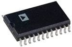
| 供应商器件封装 | 24-TSSOP-EP |
| 分辨率 | 16 bit |
| 包装 | 管件 |
| 商标 | Analog Devices |
| 安装类型 | 表面贴装 |
| 安装风格 | SMD/SMT |
| 封装 | Tube |
| 封装/外壳 | 24-TSSOP(0.173",4.40mm 宽)裸焊盘 |
| 封装/箱体 | TSSOP-24 |
| 工作温度 | -40°C ~ 85°C |
| 工厂包装数量 | 62 |
| 建立时间 | 10µs |
| 接口类型 | SPI |
| 数据接口 | 串行 |
| 最大功率耗散 | 190 mW |
| 最大工作温度 | + 85 C |
| 最小工作温度 | - 40 C |
| 标准包装 | 62 |
| 电压参考 | External |
| 电压源 | 模拟和数字,双 ± |
| 电源电压-最大 | 5.5 V |
| 电源电压-最小 | 2.7 V |
| 积分非线性 | +/- 16 LSB |
| 稳定时间 | 10 us |
| 系列 | AD5752 |
| 结构 | Resistor String |
| 设计资源 | |
| 转换器数 | 2 |
| 转换器数量 | 2 |
| 输出数和类型 | 2 电压,单极2 电压,双极 |
| 输出类型 | Voltage |
| 采样比 | 1 MSPs |
| 采样率(每秒) | * |


- 商务部:美国ITC正式对集成电路等产品启动337调查
- 曝三星4nm工艺存在良率问题 高通将骁龙8 Gen1或转产台积电
- 太阳诱电将投资9.5亿元在常州建新厂生产MLCC 预计2023年完工
- 英特尔发布欧洲新工厂建设计划 深化IDM 2.0 战略
- 台积电先进制程称霸业界 有大客户加持明年业绩稳了
- 达到5530亿美元!SIA预计今年全球半导体销售额将创下新高
- 英特尔拟将自动驾驶子公司Mobileye上市 估值或超500亿美元
- 三星加码芯片和SET,合并消费电子和移动部门,撤换高东真等 CEO
- 三星电子宣布重大人事变动 还合并消费电子和移动部门
- 海关总署:前11个月进口集成电路产品价值2.52万亿元 增长14.8%


PDF Datasheet 数据手册内容提取
Complete, Dual, 12-/14-/16-Bit, Serial Input, Unipolar/Bipolar, Voltage Output DACs Data Sheet AD5722/AD5732/AD5752 FEATURES GENERAL DESCRIPTION Complete, dual, 12-/14-/16-bit digital-to-analog converter (DAC) The AD5722/AD5732/AD5752 are dual, 12-/14-/16-bit, serial Operates from single/dual supplies input, voltage output, digital-to-analog converters. They operate Software programmable output range from single-supply voltages from +4.5 V up to +16.5 V or dual- +5 V, +10 V, +10.8 V, ±5 V, ±10 V, ±10.8 V supply voltages from ±4.5 V up to ±16.5 V. Nominal full-scale INL error: ±16 LSB maximum, DNL error: ±1 LSB maximum output range is software-selectable from +5 V, +10 V, +10.8 V, Total unadjusted error (TUE): 0.1% FSR maximum ±5 V, ±10 V, or ±10.8 V. Integrated output amplifiers, reference Settling time: 10 μs typical buffers, and proprietary power-up/power-down control circuitry Integrated reference buffers are also provided. Output control during power-up/brownout The parts offer guaranteed monotonicity, integral nonlinearity Simultaneous updating via LDAC (INL) of ±16 LSB maximum, low noise, and 10 μs typical Asynchronous CLR to zero scale or midscale settling time. DSP-/microcontroller-compatible serial interface 24-lead TSSOP The AD5722/AD5732/AD5752 use a serial interface that Operating temperature range: −40°C to +85°C operates at clock rates up to 30 MHz and are compatible with iCMOS process technology1 DSP and microcontroller interface standards. Double buffering allows the simultaneous updating of all DACs. The input coding APPLICATIONS is user-selectable twos complement or offset binary for a bipolar Industrial automation output (depending on the state of Pin BIN/2sComp), and Closed-loop servo control, process control straight binary for a unipolar output. The asynchronous clear Automotive test and measurement function clears all DAC registers to a user-selectable zero-scale Programmable logic controllers or midscale output. The parts are available in a 24-lead TSSOP and offer guaranteed specifications over the −40°C to +85°C industrial temperature range. The AD5722/AD5732/AD5752 are pin compatible with the AD5724/AD5734/AD5754, which are complete, quad, 12-/14-/ 16-bit, serial input, unipolar/bipolar voltage output DACs. FUNCTIONAL BLOCK DIAGRAM AVSS AVDD REFIN DVCC AD5722/AD5732/AD5752 REFERENCE CLR BUFFERS BIN/2sCOMP 12/14/16 12/14/16 INPUT DAC SDIN INPUTSHIFT REGISTER A REGISTER A DACA VOUTA REGISTER SCLK AND SYNC CONTROL INPUT DAC 12/14/16 LOGIC REGISTER B REGISTER B DACB VOUTB SDO GND LDAC DAC_GND (2) SIG_GND (2) 06467-001 Figure 1. 1 For analog systems designers within industrial/instrumentation equipment OEMs who need high performance ICs at higher voltage levels, iCMOS® is a technology platform that enables the development of analog ICs capable of 30 V and operating at ±15 V supplies while allowing dramatic reductions in power consumption and package size, as well as increased ac and dc performance. Rev. F Document Feedback Information furnished by Analog Devices is believed to be accurate and reliable. However, no responsibility is assumed by Analog Devices for its use, nor for any infringements of patents or other One Technology Way, P.O. Box 9106, Norwood, MA 02062-9106, U.S.A. rights of third parties that may result from its use. Specifications subject to change without notice. No license is granted by implication or otherwise under any patent or patent rights of Analog Devices. Tel: 781.329.4700 ©2008–2017 Analog Devices, Inc. All rights reserved. Trademarks and registered trademarks are the property of their respective owners. Technical Support www.analog.com
AD5722/AD5732/AD5752 Data Sheet TABLE OF CONTENTS Features .............................................................................................. 1 Transfer Function ....................................................................... 20 Applications ....................................................................................... 1 Input Shift Register .................................................................... 24 General Description ......................................................................... 1 DAC Register .............................................................................. 25 Functional Block Diagram .............................................................. 1 Output Range Select Register ................................................... 25 Revision History ............................................................................... 2 Control Register ......................................................................... 26 Specifications ..................................................................................... 3 Power Control Register ............................................................. 26 AC Performance Characteristics ................................................ 5 Design Features ............................................................................... 27 Timing Characteristics ................................................................ 5 Analog Output Control ............................................................. 27 Timing Diagrams .......................................................................... 6 Power-Down Mode .................................................................... 27 Absolute Maximum Ratings ............................................................ 8 Overcurrent Protection ............................................................. 27 ESD Caution .................................................................................. 8 Thermal Shutdown .................................................................... 27 Pin Configuration and Function Descriptions ............................. 9 Applications Information .............................................................. 28 Typical Performance Characteristics ........................................... 10 +5 V/±5 V Operation ................................................................ 28 Terminology .................................................................................... 16 Alternative Power-Up Sequence Support ............................... 28 Theory of Operation ...................................................................... 18 Layout Guidelines....................................................................... 28 Architecture ................................................................................. 18 Galvanically Isolated Interface ................................................. 29 Power-Up Sequence ................................................................... 18 Voltage Reference Selection ...................................................... 29 Serial Interface ............................................................................ 18 Microprocessor Interfacing ....................................................... 29 Load DAC (LDAC) ..................................................................... 20 Outline Dimensions ....................................................................... 31 Asynchronous Clear (CLR) ....................................................... 20 Ordering Guide .......................................................................... 31 Configuring the AD5722/AD5732/AD5752 .......................... 20 REVISION HISTORY 2/2017—Rev. E to Rev. F 3/2011—Rev. B to Rev. C Added Power-Up Sequence Section ............................................. 18 Changes to Configuring the AD5722/AD5732/AD5752 Section .. 20 Changes to Table 7 and Table 8 ..................................................... 21 Changes to Table 10 and Table 11 ................................................ 22 8/2010—Rev. A to Rev. B Changes to Table 13 and Table 14 ................................................ 23 Changes to Table 27 ....................................................................... 26 Changes to Analog Output Control Section ............................... 27 Added Alternative Power-Up Sequence Support Section, 5/2010—Rev. 0 to Rev. A Figure 43, and Figure 44; Renumbered Sequentially ................. 28 Changes to Junction Temperature, T max Parameter, Table 4 ... 8 J Changes to Exposed Paddle Description, Table 5 ......................... 9 2/2016—Rev. D to Rev. E Changes to Ordering Guide .......................................................... 30 Changes to Table 1 ............................................................................ 3 10/08—Revision 0: Initial Version 7/2011—Rev. C to Rev. D Changes to Table 3: t7, t8, t10 Limits ...................................................... 5 Rev. F | Page 2 of 31
Data Sheet AD5722/AD5732/AD5752 SPECIFICATIONS AV = 4.5 V1 to 16.5 V; AV = −4.5 V1 to −16.5 V, or AV = 0 V; GND = 0 V; REFIN = 2.5 V; DV = 2.7 V to 5.5 V; R = 2 kΩ; DD SS SS CC LOAD C = 200 pF; all specifications T to T , unless otherwise noted. LOAD MIN MAX Table 1. Parameter Min Typ Max Unit Test Conditions/Comments ACCURACY Outputs unloaded Resolution AD5752 16 Bits AD5732 14 Bits AD5722 12 Bits Total Unadjusted Error (TUE) B Version −0.1 +0.1 % FSR ±10 V range A Version −0.3 +0.3 % FSR ±10 V range Integral Nonlinearity (INL)2 AD5752 A, B Versions −16 +16 LSB AD5732 A Version −4 +4 LSB AD5722 A Version −1 +1 LSB Differential Nonlinearity (DNL) −1 +1 LSB All models, all versions, guaranteed monotonic Bipolar Zero Error −6 +6 mV ±10 V range, T = 25°C, error at other temperatures A obtained using bipolar zero TC Bipolar Zero TC3 ±4 ppm FSR/°C Zero-Scale Error −6 +6 mV ±10 V range, T = 25°C, error at other temperatures A obtained using zero-scale TC Zero-Scale TC3 ±4 ppm FSR/°C Offset Error −6 +6 mV +10 V range, T = 25°C, error at other temperatures A obtained using zero-scale TC Offset Error TC ±4 ppm FSR/°C Gain Error −0.025 +0.025 % FSR ±10 V range, T = 25°C, error at other temperatures A obtained using gain TC Gain Error3 −0.065 0 +10 V and +5 V ranges, T = 25°C, error at other A temperatures obtained using gain TC Gain Error3 0 0.08 ±5 V range, T = 25°C, error at other temperatures A obtained using gain TC Gain TC3 ±4 ppm FSR/°C DC Crosstalk3 120 μV REFERENCE INPUT3 Reference Input Voltage 2.5 V ±1% for specified performance DC Input Impedance 1 5 MΩ Input Current −2 ±0.5 +2 μA Reference Range 2 3 V OUTPUT CHARACTERISTICS3 Output Voltage Range −10.8 +10.8 V AV /AV = ±11.7 V min, REFIN = +2.5 V DD SS −12 +12 V AV /AV = ±12.9 V min, REFIN = +3 V DD SS Headroom Required 0.5 0.9 V Output Voltage TC ±4 ppm FSR/°C Output Voltage Drift vs. Time ±50 ppm FSR Drift after 1000 hours of life test @ 125°C Short-Circuit Current 20 mA Load 2 kΩ For specified performance Capacitive Load Stability 4000 pF DC Output Impedance 0.5 Ω Rev. F | Page 3 of 31
AD5722/AD5732/AD5752 Data Sheet Parameter Min Typ Max Unit Test Conditions/Comments DIGITAL INPUTS3 DV = 2.7 V to 5.5 V, JEDEC compliant CC Input High Voltage, V 2 V IH Input Low Voltage, V 0.8 V IL Input Current ±1 μA Per pin Pin Capacitance 5 pF Per pin DIGITAL OUTPUTS (SDO)3 Output Low Voltage, V 0.4 V DV = 5 V ± 10%, sinking 200 μA OL CC Output High Voltage, V DV − 1 V DV = 5 V ± 10%, sourcing 200 μA OH CC CC Output Low Voltage, V 0.4 V DV = 2.7 V to 3.6 V, sinking 200 μA OL CC Output High Voltage, V DV − 0.5 V DV = 2.7 V to 3.6 V, sourcing 200 μA OH CC CC High Impedance Leakage −1 +1 μA Current High Impedance Output 5 pF Capacitance POWER REQUIREMENTS AV 4.5 16.5 V DD AV −4.5 −16.5 V SS DV 2.7 5.5 V CC Power Supply Sensitivity3 ∆V /∆ΑV −65 dB OUT DD AI 3.25 mA/channel Outputs unloaded DD 2.4 mA/channel AV = 0 V, outputs unloaded SS AI 2.5 mA/channel Outputs unloaded SS DI 0.5 3 μA V = DV , V = GND CC IH CC IL Power Dissipation 190 mW ±16.5 V operation, outputs unloaded 79 mW 16.5 V operation, AV = 0 V, outputs unloaded SS Power-Down Currents AI 40 μA DD AI 40 μA SS D 300 nA ICC 1 For specified performance, the maximum headroom requirement is 0.9 V. 2 INL is the relative accuracy. It is measured from Code 512, Code 128, and Code 32 for the AD5752, the AD5732, and the AD5722, respectively. 3 Guaranteed by characterization; not production tested. Rev. F | Page 4 of 31
Data Sheet AD5722/AD5732/AD5752 AC PERFORMANCE CHARACTERISTICS AV = 4.5 V1 to 16.5 V; AV = −4.5 V to −16.5 V, or AV = 0 V; GND = 0 V; REFIN = 2.5 V; DV = 2.7 V to 5.5 V; R = 2 kΩ; DD SS SS CC LOAD C = 200 pF; all specifications T to T , unless otherwise noted. LOAD MIN MAX Table 2. Parameter2 Min Typ Max Unit Test Conditions/Comments DYNAMIC PERFORMANCE Output Voltage Settling Time 10 12 μs 20 V step to ±0.03% FSR 7.5 8.5 μs 10 V step to ±0.03% FSR 5 μs 512 LSB step settling (16-bit resolution) Slew Rate 3.5 V/μs Digital-to-Analog Glitch Energy 13 nV-sec Glitch Impulse Peak Amplitude 35 mV Digital Crosstalk 10 nV-sec DAC-to-DAC Crosstalk 10 nV-sec Digital Feedthrough 0.6 nV-sec Output Noise 0.1 Hz to 10 Hz Bandwidth 15 μV p-p 0x8000 DAC code 100 kHz Bandwidth 80 μV rms Output Noise Spectral Density 320 nV/√Hz Measured at 10 kHz, 0x8000 DAC code 1 For specified performance, the maximum headroom requirement is 0.9 V. 2 Guaranteed by design and characterization; not production tested. TIMING CHARACTERISTICS AV = 4.5 V to 16.5 V; AV = −4.5 V to −16.5 V, or AV = 0 V; GND = 0 V; REFIN = 2.5 V; DV = 2.7 V to 5.5 V; R = 2 kΩ; C = DD SS SS CC LOAD LOAD 200 pF; all specifications t to t , unless otherwise noted. MIN MAX Table 3. Parameter1, 2, 3 Limit at t , t Unit Description MIN MAX t 33 ns min SCLK cycle time 1 t 13 ns min SCLK high time 2 t 13 ns min SCLK low time 3 t 13 ns min SYNC falling edge to SCLK falling edge setup time 4 t 13 ns min SCLK falling edge to SYNC rising edge 5 t 100 ns min Minimum SYNC high time (write mode) 6 t 7 ns min Data setup time 7 t 2 ns min Data hold time 8 t 20 ns min LDAC falling edge to SYNC falling edge 9 t 130 ns min SYNC rising edge to LDAC falling edge 10 t 20 ns min LDAC pulse width low 11 t 10 μs max DAC output settling time 12 t 20 ns min CLR pulse width low 13 t 2.5 μs max CLR pulse activation time 14 t 4 13 ns min SYNC rising edge to SCLK falling edge 15 t 4 40 ns max SCLK rising edge to SDO valid (C 5 = 15 pF) 16 L SDO t 200 ns min Minimum SYNC high time (readback/daisy-chain mode) 17 1 Guaranteed by characterization; not production tested. 2 All input signals are specified with tR = tF = 5 ns (10% to 90% of DVCC) and timed from a voltage level of 1.2 V. 3 See Figure 2, Figure 3, and Figure 4. 4 Daisy-chain and readback mode. 5 CL SDO = capacitive load on SDO output. Rev. F | Page 5 of 31
AD5722/AD5732/AD5752 Data Sheet TIMING DIAGRAMS t1 SCLK 1 2 24 t6 t3 t2 t4 t5 SYNC t8 t7 SDIN DB23 DB0 t9 t10 t11 LDAC t12 VOUTx t12 VOUTx CLR t13 t14 VOUTx 06467-002 Figure 2. Serial Interface Timing Diagram t1 SCLK 24 48 t17 t3 t2 t5 t4 t15 SYNC t8 t7 SDIN D32B D0B D32B D0B INPUT WORD FOR DAC N INPUT WORD FOR DAC N – 1 t16 SDO DB23 DB0 UNDEFINED INPUT WORD FOR DAC N t10 t11 LDAC 06467-003 Figure 3. Daisy-Chain Timing Diagram Rev. F | Page 6 of 31
Data Sheet AD5722/AD5732/AD5752 SCLK 1 24 1 24 t17 SYNC SDIN DB23 DB0 DB23 DB0 INPUT WORD SPECIFIES NOP CONDITION REGISTER TO BE READ SDO DB23 DB0 DB23 DB0 UNDEFINED SELECCTLEOD CRKEEGDIS OTUETR DATA 06467-004 Figure 4. Readback Timing Diagram Rev. F | Page 7 of 31
AD5722/AD5732/AD5752 Data Sheet ABSOLUTE MAXIMUM RATINGS T = 25°C unless otherwise noted. A Stresses at or above those listed under Absolute Maximum Transient currents of up to 100 mA do not cause SCR latch-up. Ratings may cause permanent damage to the product. This is a stress rating only; functional operation of the product at these Table 4. or any other conditions above those indicated in the operational Parameter Rating section of this specification is not implied. Operation beyond AV to GND −0.3 V to +17 V DD the maximum operating conditions for extended periods may AV to GND +0.3 V to −17 V SS affect product reliability. DV to GND −0.3 V to +7 V CC Digital Inputs to GND −0.3 V to DV + 0.3 V or 7 V CC ESD CAUTION (whichever is less) Digital Outputs to GND −0.3 V to DV + 0.3 V or 7 V CC (whichever is less) REFIN to GND −0.3 V to +5 V V A or V B to GND AV to AV OUT OUT SS DD DAC_GND to GND −0.3 V to +0.3 V SIG_GND to GND −0.3 V to +0.3 V Operating Temperature Range, T A Industrial −40°C to +85°C Storage Temperature Range −65°C to +150°C Junction Temperature, T max 150°C J 24-Lead TSSOP Package θ Thermal Impedance 42°C/W JA θ Thermal Impedance 9°C/W JC Power Dissipation (T max − T )/θ J A JA Lead Temperature JEDEC industry standard Soldering J-STD-020 ESD (Human Body Model) 3.5 kV Rev. F | Page 8 of 31
Data Sheet AD5722/AD5732/AD5752 PIN CONFIGURATION AND FUNCTION DESCRIPTIONS AVSS 1 24 AVDD NC 2 23 VOUTB VOUTA 3 AADD55772322// 22 NC NC 4 AD5752 21 SIG_GND BIN/2sCOMP 5 20 SIG_GND TOP VIEW NC 6 (Not to Scale) 19 DAC_GND SYNC 7 18 DAC_GND SCLK 8 17 REFIN SDIN 9 16 SDO LDAC 10 15 GND CLR 11 14 DVCC NC 12 13 NC NOTES 1. NC = NO CONNECT 2. IT IS RECOMMENDED THAT THE EXPOSEDPAD BE THERMALLY CFPOEORRNF NEOENRCHMTAEANDNCCTEEOD. AT HCEORPMPAELR PLANE 06467-005 Figure 5. Pin Configuration Table 5. Pin Function Descriptions Pin No. Mnemonic Description 1 AV Negative Analog Supply. Voltage ranges from −4.5 V to −16.5 V. This pin can be connected to 0 V if output SS ranges are unipolar. 2, 4, 6, 12, NC Do not connect to these pins. 13, 22 3 V A Analog Output Voltage of DAC A. The output amplifier is capable of directly driving a 2 kΩ, 4000 pF load. OUT 5 BIN/2sCOMP Determines the DAC coding for a bipolar output range. This pin should be hardwired to either DV or GND. CC When hardwired to DV , input coding is offset binary. When hardwired to GND, input coding is twos CC complement. (For unipolar output ranges, coding is always straight binary.) 7 SYNC Active Low Input. This is the frame synchronization signal for the serial interface. While SYNC is low, data is transferred on the falling edge of SCLK. Data is latched on the rising edge of SYNC. 8 SCLK Serial Clock Input. Data is clocked into the shift register on the falling edge of SCLK. This operates at clock speeds up to 30 MHz. 9 SDIN Serial Data Input. Data must be valid on the falling edge of SCLK. 10 LDAC Load DAC, Logic Input. This is used to update the DAC registers and, consequently, the analog outputs. When this pin is tied permanently low, the addressed DAC register is updated on the rising edge of SYNC. If LDAC is held high during the write cycle, the DAC input register is updated, but the output update is held off until the falling edge of LDAC. In this mode, all analog outputs can be updated simultaneously on the falling edge of LDAC. The LDAC pin should not be left unconnected. 11 CLR Active Low Input. Asserting this pin sets the DAC registers to zero-scale code or midscale code (user-selectable). 14 DV Digital Supply. Voltage ranges from 2.7 V to 5.5 V. CC 15 GND Ground Reference. 16 SDO Serial Data Output. Used to clock data from the serial register in daisy-chain or readback mode. Data is clocked out on the rising edge of SCLK and is valid on the falling edge of SCLK. 17 REFIN External Reference Voltage Input. Reference input range is 2 V to 3 V. REFIN = 2.5 V for specified performance. 18, 19 DAC_GND Ground Reference for the Two Digital-to-Analog Converters (DACs). 20, 21 SIG_GND Ground Reference for the Two Output Amplifiers. 23 V B Analog Output Voltage of DAC B. The output amplifier is capable of directly driving a 2 kΩ, 4000 pF load. OUT 24 AV Positive Analog Supply. Voltage ranges from 4.5 V to 16.5 V. DD Exposed This exposed paddle should be connected to the potential of the AV pin, or alternatively, it can be left electrically SS Paddle unconnected. It is recommended that the paddle be thermally connected to a copper plane for enhanced thermal performance. Rev. F | Page 9 of 31
AD5722/AD5732/AD5752 Data Sheet TYPICAL PERFORMANCE CHARACTERISTICS 6 0.6 AVDD/AVSS = +12V/0V, RANGE = +10V AVDD/AVSS = ±12V, RANGE = ±10V 4 AVDD/AVSS = ±6.5V, RANGE = ±5V 0.4 AVDD/AVSS = +6.5V/0V, RANGE = +5V 2 0.2 B) B) R (LS 0 R (LS 0 O O R R NL ER –2 NL ER–0.2 I D –4 –0.4 –6 –0.6 AAVVDDDD//AAVVSSSS == +±1122VV,/ 0RVA, NRGAEN G= E± 1=0 +V10V AVDD/AVSS = ±6.5V, RANGE = ±5V AVDD/AVSS = +6.5V/0V, RANGE = +5V –8 –0.8 0 10,000 20,000 30,C00O0DE40,000 50,000 60,000 06467-013 0 10,000 20,000 30,C00O0DE40,000 50,000 60,000 06467-016 Figure 6. AD5752 Integral Nonlinearity Error vs. Code Figure 9. AD5752 Differential Nonlinearity Error vs. Code 1.5 0.15 AVDD/AVSS = +12V/0V, RANGE = +10V AVDD/AVSS = ±12V, RANGE = ±10V 1.0 AAVVDDDD//AAVVSSSS == ±+66..55VV,/ 0RVA, NRGAEN G= E± 5=V +5V 0.10 0.5 0.05 B) B) S S R (L 0 R (L 0 O O R R NL ER–0.5 NL ER–0.05 I D –1.0 –0.10 –1.5 –0.15 AAVVDDDD//AAVVSSSS == +±1122VV,/ 0RVA, NRGAEN G=E ± 1=0 +V10V AVDD/AVSS = ±6.5V, RANGE = ±5V AVDD/AVSS = +6.5V/0V, RANGE = +5V –2.0 –0.20 0 2000 4000 6000 C80O0D0E10,000 12,000 14,000 16,000 06467-014 0 2000 4000 6000 8C0O0D0E10,000 12,000 14,000 16,000 06467-017 Figure 7. AD5732 Integral Nonlinearity Error vs. Code Figure 10. AD5732 Differential Nonlinearity Error vs. Code 0.3 0.04 AVDD/AVSS = +12V/0V, RANGE = +10V AVDD/AVSS = +12V/0V, RANGE = +10V AVDD/AVSS = ±12V, RANGE = ±10V AVDD/AVSS = ±12V, RANGE = ±10V 0.2 AVDD/AVSS = ±6.5V, RANGE = ±5V 0.03 AVDD/AVSS = ±6.5V, RANGE = ±5V AVDD/AVSS = +6.5V/0V, RANGE = +5V AVDD/AVSS = +6.5V/0V, RANGE = +5V 0.02 0.1 B) B) 0.01 R (LS 0 R (LS 0 INL ERRO––00..21 DNL ERRO ––00..0021 –0.3 –0.03 –0.4 –0.04 –0.5 –0.05 0 500 1000 1500 C20O0D0E 2500 3000 3500 4000 06467-015 0 500 1000 1500 C20O0D0E 2500 3000 3500 4000 06467-018 Figure 8. AD5722 Integral Nonlinearity Error vs. Code Figure 11. AD5722 Differential Nonlinearity Error vs. Code Rev. F | Page 10 of 31
Data Sheet AD5722/AD5732/AD5752 8 10 8 6 6 4 LSB) 2 MMMAAINXX I NIINNLLL ± ±±11500VVV LSB) 24 ROR ( 0 MMMAIINNX II NNINLLL ±+ +511V00VV ROR ( 0 BUBINIPPIOOPOLLAALARRR 55 VV5 VMM MIANXIN L ER –2 MMAINX I NINLL + +55VV L ER –2 UNIPOLAR 5V MAX N N I I –4 –4 –6 –6 –8 –8 –10 –40 –20 0TEMPER2A0TURE (°4C0) 60 80 06467-044 5.5 6.5 7.5 8.5 S9U.P5PL1Y0 .V5OL11T.A5GE12 (.V5)13.5 14.5 15.5 16.5 06467-035 Figure 12. AD5752 Integral Nonlinearity Error vs. Temperature Figure 15. AD5752 Integral Nonlinearity Error vs. Supply Voltage 0.1 1.0 BIPOLAR 10V MIN 0.8 UNIPOLAR 10V MIN 0 BIPOLAR 10V MAX UNIPOLAR 10V MAX 0.6 –0.1 MAX DNL ±10V 0.4 B) MAX DNL ±5V B) S MIN DNL ±10V S R (L–0.2 MMIANX D DNNLL ± +51V0V R (L 0.2 RO MIN DNL +10V RO 0 R MAX DNL +5V R NL E–0.3 MIN DNL +5V NL E–0.2 D D –0.4 –0.4 –0.6 –0.5 –0.8 –0.6–40 –20 0TEMPER2A0TURE (°4C0) 60 80 06467-045 –1.011.5 12.0 12.5 13.0SUP13P.L5Y V1O4.L0TA1G4E.5 (V1)5.0 15.5 16.0 16.5 06467-032 Figure 13. AD5752 Differential Nonlinearity Error vs. Temperature Figure 16. AD5752 Differential Nonlinearity Error vs. Supply Voltage 1.0 10 BIPOLAR 5V MIN 0.8 UNIPOLAR 5V MIN 8 BIPOLAR 5V MAX UNIPOLAR 5V MAX 0.6 6 0.4 4 B) ROR (LSB) 02 BUBINIPPIOOPOLLAALRRA R11 001VV0 VMM MIANIXN RROR (LS 0.20 INL ER ––42 UNIPOLAR 10V MAX DNL E––00..42 –0.6 –6 –0.8 –8 –1.0 –1011.5 12.0 12.5 13.0SUP13P.L5Y V14O.L0TA1G4.E5 (V1)5.0 15.5 16.0 16.5 06467-034 Figu5.r5e 176. .A5D577.552 D8i.f5ferSe9Un.P5tiPaLl1 NY0 o.V5nOliL1n1Te.A5aGritE1y2 (.EV5r)ro1r3 v.5s. S1u4p.5ply1 5V.o5lta1g6.e5 06467-033 Figure 14. AD5752 Integral Nonlinearity Error vs. Supply Voltage Rev. F | Page 11 of 31
AD5722/AD5732/AD5752 Data Sheet 0.02 6.0 5.5 0.01 5.0 0 BIPOLAR 10V MIN UNIPOLAR 10V MIN 4.5 %) BUINPIOPOLALRA R1 01V0 VM MAXAX mA) E ( –0.01 (D 4.0 U D T AI 3.5 –0.02 3.0 –0.03 2.5 –0.04 2.0 11.5 12.0 12.5 13.0SUP13P.L5Y V14O.L0TA1G4.E5 (V1)5.0 15.5 16.0 16.5 06467-036 4.5 6.5 8.5 AV1D0D.5 (V) 12.5 14.5 16.5 06467-042 Figure 18. AD5752 Total Unadjusted Error vs. Supply Voltage Figure 21. Supply Current vs. Supply Voltage (Single Supply) 0.04 4 0.03 +10V 3 0.02 V) m 2 0.01 BIPOLAR 5V MIN R ( UNIPOLAR 5V MIN O E (%) 0 BUINPIOPOLALRA R5 V5 VM MAXAX E ERR 1 ±10V TU –0.01 AL 0 C S –0.02 O- ER –1 –0.03 Z –2 –0.04 ±5V –0.055.5 6.5 7.5 8.5 S9U.P5PL1Y0 .V5OL11T.A5G1E2 (.V5)13.5 14.5 15.5 16.5 06467-037 –3–40 –20 0TEMPER2A0TURE (°4C0) 60 80 06467-046 Figure 19. AD5752 Total Unadjusted Error vs. Supply Voltage Figure 22. Zero-Scale Error vs. Temperature 5 0.8 4 0.6 AIDD (mA) 3 V) 0.4 m A) 2 OR ( 0.2 ±5V RANGE m R (S 1 ER 0 /AIDS 0 ERO –0.2 ±10V RANGE D Z AI R –1 LA–0.4 O –2 AIDD (mA) BIP–0.6 –3 –0.8 –4 F4i.g5ure 20. 6S.u5pply Cu8r.r5enAtV vDsD. 1/SA0u.V5pSpSl y(V V)o1l2ta.5ge (Du1a4l. S5upply)1 6.5 06467-038 –1.0–40 –20 0TEMPER2A0TURE (°4C0) 60 80 06467-047 Figure 23. Bipolar Zero Error vs. Temperature Rev. F | Page 12 of 31
Data Sheet AD5722/AD5732/AD5752 0.06 15 ±5V 0.04 10 % FSR)0.02 AGE (V) 5 R ( LT O 0 O 0 R ±10V V ER UT N P GAI–0.02 OUT –5 +10V –0.04 –10 –0.06–40 –20 0TEMPER2A0TURE (°4C0) 60 80 06467-048 –15–3 –1 1 3 TIME (5µs) 7 9 11 06467-022 Figure 24. Gain Error vs. Temperature Figure 27. Full-Scale Settling Time, ±10 V Range 1000 7 900 5 800 700 V) 3 600 E ( G (µA)C500 OLTA 1 DIC340000 DVCC = 5V PUT V –1 T U 200 O –3 100 DVCC = 3V –5 0 –100 0 Figure 125. Digita2l CurrVeLnOtG v3IsC. (LVo)gic In4put Volta5ge 6 06467-043 –7–3 –1 1 3 TIME (5µs) 7 9 11 06467-023 Figure 28. Full-Scale Settling Time, ±5 V Range 0.010 ±5V RANGE, CODE = 0xFFFF 12 ±10V RANGE, CODE = 0xFFFF +10V RANGE, CODE = 0xFFFF 0.005 +5V RANGE, CODE = 0xFFFF A (V) ±±51V0V R RAANNGGEE, ,C COODDEE = = 0 x00x0000000 10 LT 0 V) DE E ( 8 UTPUT VOLTAGE ––00..001005 OUTPUT VOLTAG 46 O –0.015 2 –0.020 –25 Fi–g2u0re 2–615. Ou–t1pO0uUtT SP–oU5uTr cCeU 0aRnRdE NST5in (km CAa1)0pabi1li5ty 20 25 06467-040 0–3 –1 1 3 TIME (5µs) 7 9 11 06467-024 Figure 29. Full-Scale Settling Time, +10 V Range Rev. F | Page 13 of 31
AD5722/AD5732/AD5752 Data Sheet 6 5 V) E ( 4 G A T L O 3 V UT 1 P UT 2 O 1 0 RANGE = ±5V RANGE = +10V –3 –1 1 3 TIME (5µs) 7 9 11 06467-025 CH1 R5AµVNGE = +5V RANGEM =5 s±10V LINE 73.8V 06467-027 Figure 30. Full-Scale Settling Time, +5 V Range Figure 33. Peak-to-Peak Noise, 100 kHz Bandwidth 0.020 0.10 ±10V RANGE, 0x7FF±F TO 0x8000 AVDD/AVSS = ±16.5V ±10V RANGE, 0x8000 TO 0x7FFF AVDD = +16.5V, AVSS = 0V ±5V RANGE, 0x7FFF TO 0x8000 0.08 0.015 ±5V RANGE, 0x8000 TO 0x7FFF +10V RANGE, 0x7FFF TO 0x8000 +10V RANGE, 0x8000 TO 0x7FFF 0.06 V) 0.010 +5V RANGE, 0x7FFF TO 0x8000 V) GE ( +5V RANGE, 0x8000 TO 0x7FFF GE ( 0.04 TA 0.005 TA L L O O 0.02 V V UT 0 UT P P 0 T T U U O–0.005 O –0.02 –0.010 –0.04 –0.015–1 0 1 TIME2 (µs) 3 4 5 06467-039 –0.06–50 –30 –10 10TIME 3(µ0s) 50 70 90 06467-041 Figure 31. Digital-to-Analog Glitch Energy Figure 34. Output Glitch on Power-Up 15 AVDD/AVSS = +12V/0V, RANGE = +10V 10 AAVVDDDD//AAVVSSSS == ±±16.25VV,, RRAANNGGEE = = ± ±150VV AVDD/AVSS = +6.5V/0V, RANGE = +5V 5 0 B) –5 S E (L –10 1 TU –15 –20 –25 –30 CH1 5RRµAAVNNGGEE == +±55VV RRAANNGGMEE ==5 s+±1100VV LINE 73.8V 06467-026 –350 1000 2000 30C00ODE 4000 5000 6000 06467-019 Figure 32. Peak-to-Peak Noise, 0.1 Hz to 10 Hz Bandwidth Figure 35. AD5752 Total Unadjusted Error vs. Code Rev. F | Page 14 of 31
Data Sheet AD5722/AD5732/AD5752 4 1.0 AVDD/AVSS = +12V/0V, RANGE = +10V AVDD/AVSS = +12V/0V, RANGE = +10V AVDD/AVSS = ±12V, RANGE = ±10V AVDD/AVSS = ±12V, RANGE = ±10V 2 AAVVDDDD//AAVVSSSS == ±+66..55VV,/ 0RVA, NRGAEN G=E ± 5=V +5V 0.5 AAVVDDDD//AAVVSSSS == ±+66..55VV,/ 0RVA, NRGAEN G=E ± 5=V +5V 0 0 B) –2 B)–0.5 S S TUE (L –4 TUE (L–1.0 –6 –1.5 –8 –2.0 –100 2000 4000 6000 C80O0D0E 10000 12000 14000 16000 06467-020 –2.50 500 1000 1500 C20O0D0E 2500 3000 3500 4000 06467-021 Figure 36. AD5732 Total Unadjusted Error vs. Code Figure 37. AD5722 Total Unadjusted Error vs. Code Rev. F | Page 15 of 31
AD5722/AD5732/AD5752 Data Sheet TERMINOLOGY Relative Accuracy or Integral Nonlinearity (INL) Gain Error For the DAC, relative accuracy, or integral nonlinearity, is a Gain error is a measure of the span error of the DAC. It is the measure of the maximum deviation in LSBs from a straight line deviation in slope of the DAC transfer characteristic from the passing through the endpoints of the DAC transfer function. A ideal and is expressed in % FSR. A plot of gain error vs. typical INL vs. code plot can be seen in Figure 6. temperature can be seen in Figure 24. Differential Nonlinearity (DNL) Gain TC Differential nonlinearity is the difference between the measured Gain TC is a measure of the change in gain error with changes change and the ideal 1 LSB change between any two adjacent in temperature. Gain TC is expressed in ppm FSR/°C. codes. A specified differential nonlinearity of ±1 LSB maximum Total Unadjusted Error (TUE) ensures monotonicity. This DAC is guaranteed monotonic by Total unadjusted error is a measure of the output error taking design. A typical DNL vs. code plot can be seen in Figure 9. all the various errors into account, namely INL error, offset Monotonicity error, gain error, and output drift over supplies, temperature, A DAC is monotonic if the output either increases or remains and time. TUE is expressed in % FSR. constant for increasing digital input code. The AD5722/AD5732/ Digital-to-Analog Glitch Impulse AD5752 are monotonic over their full operating temperature Digital-to-analog glitch impulse is the impulse injected into the range. analog output when the input code in the DAC register changes Bipolar Zero Error state, but the output voltage remains constant. It is normally Bipolar zero error is the deviation of the analog output from the specified as the area of the glitch in nV-sec and is measured ideal half-scale output of 0 V when the DAC register is loaded when the digital input code is changed by 1 LSB at the major with 0x8000 (straight binary coding) or 0x0000 (twos complement carry transition (0x7FFF to 0x8000). See Figure 31. coding). A plot of bipolar zero error vs. temperature can be seen Glitch Impulse Peak Amplitude in Figure 23. Glitch impulse peak amplitude is the peak amplitude of the Bipolar Zero TC impulse injected into the analog output when the input code in Bipolar zero TC is a measure of the change in the bipolar zero the DAC register changes state. It is specified as the amplitude error with a change in temperature. It is expressed in ppm FSR/°C. of the glitch in mV and is measured when the digital input code is changed by 1 LSB at the major carry transition (0x7FFF to Zero-Scale Error or Negative Full-Scale Error 0x8000). See Figure 31. Zero-scale error is the error in the DAC output voltage when 0x0000 (straight binary coding) or 0x8000 (twos complement Digital Feedthrough coding) is loaded to the DAC register. Ideally, the output voltage Digital feedthrough is a measure of the impulse injected into should be negative full-scale − 1 LSB. A plot of zero-scale error the analog output of the DAC from the digital inputs of the vs. temperature can be seen in Figure 22. DAC but is measured when the DAC output is not updated. It is specified in nV-sec and measured with a full-scale code change Zero-Scale TC on the data bus. Zero-scale TC is a measure of the change in zero-scale error with a change in temperature. Zero-scale TC is expressed in ppm FSR/°C. Power Supply Sensitivity Power supply sensitivity indicates how the output of the DAC is Output Voltage Settling Time affected by changes in the power supply voltage. It is measured Output voltage settling time is the amount of time required for by superimposing a 50 Hz/60 Hz, 200 mV p-p sine wave on the the output to settle to a specified level for a full-scale input change. supply voltages and measuring the proportion of the sine wave A plot for full-scale settling time can be seen in Figure 27. that transfers to the outputs. Slew Rate DC Crosstalk The slew rate of a device is a limitation in the rate of change of This is the dc change in the output level of one DAC in response the output voltage. The output slewing speed of a voltage output to a change in the output of another DAC. It is measured with a DAC is usually limited by the slew rate of the amplifier used at full-scale output change on one DAC while monitoring another its output. Slew rate is measured from 10% to 90% of the output DAC. It is expressed in LSBs. signal and is given in V/μs. Rev. F | Page 16 of 31
Data Sheet AD5722/AD5732/AD5752 Digital Crosstalk DAC-to-DAC Crosstalk Digital crosstalk is a measure of the impulse injected into the DAC-to-DAC crosstalk is the glitch impulse transferred to the analog output of one DAC from the digital inputs of another output of one DAC due to a digital code change and a subsequent DAC but is measured when the DAC output is not updated. It is output change of another DAC. This includes both digital and specified in nV-sec and measured with a full-scale code change analog crosstalk. It is measured by loading one of the DACs on the data bus. with a full-scale code change (all 0s to all 1s and vice versa) with LDAC low and monitoring the output of another DAC. The energy of the glitch is expressed in nV-sec. Rev. F | Page 17 of 31
AD5722/AD5732/AD5752 Data Sheet THEORY OF OPERATION The AD5722/AD5732/AD5752 are dual, 12-/14-/16-bit, serial The resistor string structure is shown in Figure 39. It is a string input, unipolar/bipolar, voltage output DACs. They operate of resistors, each of value R. The code loaded to the DAC register from unipolar supply voltages of +4.5 V to +16.5 V or bipolar determines the node on the string where the voltage is to be supply voltages of ±4.5 V to ±16.5 V. In addition, the parts have tapped off and fed into the output amplifier. The voltage is software-selectable output ranges of +5 V, +10 V, +10.8 V, ±5 V, tapped off by closing one of the switches connecting the string ±10 V, and ±10.8 V. Data is written to the AD5722/AD5732/ to the amplifier. Because it is a string of resistors, it is guaranteed AD5752 in a 24-bit word format via a 3-wire serial interface. monotonic. The devices also offer an SDO pin to facilitate daisy-chaining Output Amplifiers or readback. The output amplifiers are capable of generating both unipolar The AD5722/AD5732/AD5752 incorporate a power-on reset and bipolar output voltages. They are capable of driving a load circuit to ensure that the DAC registers power up loaded with of 2 kΩ in parallel with 4000 pF to GND. The source and sink 0x0000. When powered on, the outputs are clamped to 0 V via capabilities of the output amplifiers can be seen in Figure 26. a low impedance path. The slew rate is 3.5 V/μs with a full-scale settling time of 10 μs. ARCHITECTURE Reference Buffers The DAC architecture consists of a string DAC followed by an The AD5722/AD5732/AD5752 require an external reference output amplifier. Figure 38 shows a block diagram of the DAC source. The reference input has an input range of 2 V to 3 V, architecture. The reference input is buffered before being with 2.5 V for specified performance. This input voltage is then applied to the DAC. buffered before it is applied to the DAC cores. REFIN POWER-UP SEQUENCE Because the DAC output voltage is controlled by the voltage REF (+) monitor and control block (see Figure 42), it is important to DAC REGISTER RSETSRISINTOGR VOUTX power the DVCC pin before applying any voltage to the AVDD and AV pins; otherwise, the G1 and G2 transmission gates are at REF (–) CONFIGURABLE SS OUTPUT an undefined state. The ideal power-up sequence is in the AMPLIFIER following order: GND, SIG_GND, DAC_GND, DV , AV , RANGEG NCDOONUTTRPOULT 06467-006 AAVVSS, aanndd tAhVen tihs en dotig iimtapl oinrtpauntts,. pTrhoev irdeeladt itvhea to rthdeeyr C oaCrf ep poowDweDreirnegd Figure 38. DAC Architecture Block Diagram DD SS up after DV . CC REFIN SERIAL INTERFACE R The AD5722/AD5732/AD5752 are controlled over a versatile 3-wire serial interface that operates at clock rates up to 30 MHz. It is compatible with SPI, QSPI™, MICROWIRE™, and DSP R standards. Input Shift Register R TO OUTPUT AMPLIFIER The input shift register is 24 bits wide. Data is loaded into the device MSB first as a 24-bit word under the control of a serial clock input, SCLK. The input register consists of a read/write bit, three register select bits, three DAC address bits, and 16 data bits. The timing diagram for this operation is shown in Figure 2. R R 06467-007 Figure 39. Resistor String Structure Rev. F | Page 18 of 31
Data Sheet AD5722/AD5732/AD5752 Standalone Operation Daisy-Chain Operation The serial interface works with both a continuous and noncon- For systems that contain several devices, the SDO pin can be tinuous serial clock. A continuous SCLK source can be used used to daisy-chain several devices together. Daisy-chain mode only if SYNC is held low for the correct number of clock cycles. can be useful in system diagnostics and in reducing the number In gated clock mode, a burst clock containing the exact number of serial interface lines. The first falling edge of SYNC starts the of clock cycles must be used, and SYNC must be taken high write cycle. SCLK is continuously applied to the input shift after the final clock to latch the data. The first falling edge of register when SYNC is low. If more than 24 clock pulses are SYNC starts the write cycle. Exactly 24 falling clock edges must applied, the data ripples out of the shift register and appears on be applied to SCLK before SYNC is brought high again. If the SDO line. This data is clocked out on the rising edge of SYNC is brought high before the 24th falling SCLK edge, the SCLK and is valid on the falling edge. By connecting the SDO of the first device to the SDIN input of the next device in the data written is invalid. If more than 24 falling SCLK edges are chain, a multidevice interface is constructed. Each device in the applied before SYNC is brought high, the input data is also system requires 24 clock pulses. Therefore, the total number of invalid. The input register addressed is updated on the rising clock cycles must equal 24 × N, where N is the total number of edge of SYNC. For another serial transfer to take place, SYNC AD5722/AD5732/AD5752 devices in the chain. When the serial must be brought low again. After the end of the serial data transfer to all devices is complete, SYNC is taken high. This transfer, data is automatically transferred from the input shift latches the input data in each device in the daisy chain and register to the addressed register. prevents any further data from being clocked into the input shift When the data has been transferred into the chosen register of register. The serial clock can be a continuous or a gated clock. the addressed DAC, all DAC registers and outputs can be A continuous SCLK source can only be used if SYNC is held updated by taking LDAC low while SYNC is high. low for the correct number of clock cycles. In gated clock mode, AD5722/ a burst clock containing the exact number of clock cycles must 68HC11* AD5732/ AD5752* be used, and SYNC must be taken high after the final clock to MOSI SDIN latch the data. SCK SCLK Readback Operation PC7 SYNC Readback mode is invoked by setting the R/W bit = 1 in the PC6 LDAC MISO SDO write operation to the serial input shift register. (If the SDO output is disabled via the SDO disable bit in the control register, it is automatically enabled for the duration of the read operation, SDIN after which it is disabled again.) With R/W = 1, Bit A2 to Bit A0, AD5722/ AD5732/ in association with Bit REG2 to Bit REG0, select the register to AD5752* be read. The remaining data bits in the write sequence are don’t SCLK care bits. During the next SPI write, the data appearing on the SDO SYNC output contains the data from the previously addressed register. LDAC For a read of a single register, the NOP command can be used in SDO clocking out the data from the selected register on SDO. The readback diagram in Figure 4 shows the readback sequence. For example, to read back the DAC register of Channel A, the SDIN AD5722/ following sequence should be implemented: AD5732/ AD5752* 1. Write 0x800000 to the AD5722/AD5732/AD5752 input SCLK register. This configures the part for read mode with the SYNC DAC register of Channel A selected. Note that all the data LDAC bits, DB15 to DB0, are don’t care bits. SDO 2. Follow this with a second write, a NOP condition, 0x180000. *ADDITIONAL PINS OMITTED FOR CLARITY. 06467-008 Donu rthineg S tDhOis wlinriet.e , the data from the register is clocked out Figure 40. Daisy Chaining the AD5722/AD5732/AD5752 Rev. F | Page 19 of 31
AD5722/AD5732/AD5752 Data Sheet LOAD DAC (LDAC) CONFIGURING THE AD5722/AD5732/AD5752 After data has been transferred into the input register of the When the power supplies are applied to the AD5722/AD5732/ DACs, there are two ways to update the DAC registers and DAC AD5752, the power-on reset circuit ensures that all registers outputs. Depending on the status of both SYNC and LDAC, one default to 0. This places all channels in power-down mode. The of two update modes is selected: individual DAC updating or DVCC should be brought high before any of the interface lines simultaneous updating of all DACs. are powered. If this is not done the first write to the device may be ignored. The first communication to the AD5722/AD5732/ OUTPUT AMPLIFIER AD5752 should be to set the required output range on all REFIN 12-/1D4-A/1C6-BIT VOUTX channels (the default range is the 5 V unipolar range) by writing to the output range select register. The user should then write to the power control register to power on the required channels. To DAC LDAC REGISTER program an output value on a channel, that channel must first be powered up; any writes to a channel while it is in power-down mode are ignored. The AD5722/AD5732/AD5752 operate with a INPUT REGISTER wide power supply range. It is important that the power supply applied to the parts provide adequate headroom to support the chosen output ranges. SSSYCDNLICNK INTLEORGFIACCE SDO 06467-009 TRANSFER FUNCTION Figure 41. Simplified Diagram of Input Loading Circuitry for One DAC Table 7 to Table 15 show the relationships of the ideal input Individual DAC Updating code to output voltage for the AD5752, AD5732, and AD5722, respectively, for all output voltage ranges. For unipolar output In this mode, LDAC is held low while data is clocked into the ranges, the data coding is straight binary. For bipolar output input shift register. The addressed DAC output is updated on ranges, the data coding is user selectable via the BIN/2sCOMP the rising edge of SYNC. pin and can be either offset binary or twos complement. Simultaneous Updating of All DACs For a unipolar output range, the output voltage expression is In this mode, LDAC is held high while data is clocked into the given by input shift register. All DAC outputs are asynchronously updated D by taking LDAC low after SYNC has been taken high. The V V Gain OUT REFIN 2N update now occurs on the falling edge of LDAC. For a bipolar output range, the output voltage expression is given by ASYNCHRONOUS CLEAR (CLR) CLR is an active low clear that allows the outputs to be cleared V V GainD GainVREFIN OUT REFIN 2N 2 to either zero-scale code or midscale code. The clear code value is user-selectable via the CLR select bit of the control register (see where: the Control Register section). It is necessary to maintain CLR low D is the decimal equivalent of the code loaded to the DAC. for a minimum amount of time to complete the operation (see N is the bit resolution of the DAC. Figure 2). When the CLR signal is returned high, the output VREFIN is the reference voltage applied at the REFIN pin. Gain is an internal gain whose value depends on the output remains at the cleared value until a new value is programmed. range selected by the user, as shown in Table 6. The outputs cannot be updated with a new value while the CLR pin is low. A clear operation can also be performed via the clear Table 6. Internal Gain Values command in the control register. Output Range (V) Gain Value +5 2 +10 4 +10.8 4.32 ±5 4 ±10 8 ±10.8 8.64 Rev. F | Page 20 of 31
Data Sheet AD5722/AD5732/AD5752 Ideal Output Voltage to Input Code Relationship—AD5752 Table 7. Bipolar Output, Offset Binary Coding Digital Input Analog Output MSB LSB ±5 V Output Range ±10 V Output Range ±10.8 V Output Range 1111 1111 1111 1111 +2 × REFIN × (32,767/32,768) +4 × REFIN × (32,767/32,768) +4.32 × REFIN × (32,767/32,768) 1111 1111 1111 1110 +2 × REFIN × (32,766/32,768) +4 × REFIN × (32,766/32,768) +4.32 × REFIN × (32,766/32,768) … … … … … … … 1000 0000 0000 0001 +2 × REFIN × (1/32,768) +4 × REFIN × (1/32,768) +4.32 × REFIN × (1/32,768) 1000 0000 0000 0000 0 V 0 V 0 V 0111 1111 1111 1111 −2 × REFIN × (1/32,768) −4 × REFIN × (1/32,768) −4.32 × REFIN × (32,766/32,768) … … … … … … … 0000 0000 0000 0001 −2 × REFIN × (32,767/32,768) −4 × REFIN × (32,767/32,768) −4.32 × REFIN × (32,767/32,768) 0000 0000 0000 0000 −2 × REFIN × (32,768/32,768) −4 × REFIN × (32,768/32,768) −4.32 × REFIN × (32,768/32,768) Table 8. Bipolar Output, Twos Complement Coding Digital Input Analog Output MSB LSB ±5 V Output Range ±10 V Output Range ±10.8 V Output Range 0111 1111 1111 1111 +2 × REFIN × (32,767/32,768) +4 × REFIN × (32,767/32,768) +4.32 × REFIN × (32,767/32,768) 0111 1111 1111 1110 +2 × REFIN × (32,766/32,768) +4 × REFIN × (32,766/32,768) +4.32 × REFIN × (32,766/32,768) … … … … … … … 0000 0000 0000 0001 +2 × REFIN × (1/32,768) +4 × REFIN × (1/32,768) +4.32 × REFIN × (1/32,768) 0000 0000 0000 0000 0 V 0 V 0 V 1111 1111 1111 1111 −2 × REFIN × (1/32,768) −4 × REFIN × (1/32,768) −4.32 × REFIN × (1/32,768) … … … … … … … 1000 0000 0000 0001 −2 × REFIN × (32,767/32,768) −4 × REFIN × (32,767/32,768) −4.32 × REFIN × (32,767/32,768) 1000 0000 0000 0000 −2 × REFIN × (32,768/32,768) −4 × REFIN × (32,768/32,768) −4.32 × REFIN × (32,768/32,768) Table 9. Unipolar Output, Straight Binary Coding Digital Input Analog Output MSB LSB +5 V Output Range +10 V Output Range +10.8 V Output Range 1111 1111 1111 1111 +2 × REFIN × (65,535/65,536) +4 × REFIN × (65,535/65,536) +4.32 × REFIN × (65,535/65,536) 1111 1111 1111 1110 +2 × REFIN × (65,534/65,536) +4 × REFIN × (65,534/65,536) +4.32 × REFIN × (65,534/65,536) … … … … … … … 1000 0000 0000 0001 +2 × REFIN × (32,769/65,536) +4 × REFIN × (32,769/65,536) +4.32 × REFIN × (32,769/65,536) 1000 0000 0000 0000 +2 × REFIN × (32,768/65,536) +4 × REFIN × (32,768/65,536) +4.32 × REFIN × (32,768/65,536) 0111 1111 1111 1111 +2 × REFIN × (32,767/65,536) +4 × REFIN × (32,767/65,536) +4.32 × REFIN × (32,767/65,536) … … … … … … … 0000 0000 0000 0001 +2 × REFIN × (1/65,536) +4 × REFIN × (1/65,536) +4.32 × REFIN × (1/65,536) 0000 0000 0000 0000 0 V 0 V 0 V Rev. F | Page 21 of 31
AD5722/AD5732/AD5752 Data Sheet Ideal Output Voltage to Input Code Relationship—AD5732 Table 10. Bipolar Output, Offset Binary Coding Digital Input Analog Output MSB LSB ±5 V Output Range ±10 V Output Range ±10.8 V Output Range 11 1111 1111 1111 +2 × REFIN × (8191/8192) +4 × REFIN × (8191/8192) +4.32 × REFIN × (8191/8192) 11 1111 1111 1110 +2 × REFIN × (8190/8192) +4 × REFIN × (8190/8192) +4.32 × REFIN × (8190/8192) … … … … … … … 10 0000 0000 0001 +2 × REFIN × (1/8192) +4 × REFIN × (1/8192) +4.32 × REFIN × (1/8192) 10 0000 0000 0000 0 V 0 V 0 V 01 1111 1111 1111 −2 × REFIN × (1/8192) −4 × REFIN × (1/8192) −4.32 × REFIN × (1/8192) … … … … … … … 00 0000 0000 0001 −2 × REFIN × (8191/8192) −4 × REFIN × (8191/8192) −4.32 × REFIN × (8191/8192) 00 0000 0000 0000 −2 × REFIN × (8192/8192) −4 × REFIN × (8192/8192) −4.32 × REFIN × (8192/8192) Table 11. Bipolar Output, Twos Complement Coding Digital Input Analog Output MSB LSB ±5 V Output Range ±10 V Output Range ±10.8 V Output Range 01 1111 1111 1111 +2 × REFIN × (8191/8192) +4 × REFIN × (8191/8192) +4.32 × REFIN × (8191/8192) 01 1111 1111 1110 +2 × REFIN × (8190/8192) +4 × REFIN × (8190/8192) +4.32 × REFIN × (8190/8192) … … … … … … … 00 0000 0000 0001 +2 × REFIN × (1/8192) +4 × REFIN × (1/8192) +4.32 × REFIN × (1/8192) 00 0000 0000 0000 0 V 0 V 0 V 11 1111 1111 1111 −2 × REFIN × (1/8192) −4 × REFIN × (1/8192) −4.32 × REFIN × (1/8192) … … … … … … … 10 0000 0000 0001 −2 × REFIN × (8191/8192) −4 × REFIN × (8191/8192) −4.32 × REFIN × (8191/8192) 10 0000 0000 0000 −2 × REFIN × (8192/8192) −4 × REFIN × (8192/8192) −4.32 × REFIN × (8192/8192) Table 12. Unipolar Output, Straight Binary Coding Digital Input Analog Output MSB LSB +5 V Output Range +10 V Output Range +10.8 V Output Range 11 1111 1111 1111 +2 × REFIN × (16,383/16,384) +4 × REFIN × (16,383/16,384) +4.32 × REFIN × (16,383/16,384) 11 1111 1111 1110 +2 × REFIN × (16,382/16,384) +4 × REFIN × (16,382/16,384) +4.32 × REFIN × (16,382/16,384) … … … … … … … 10 0000 0000 0001 +2 × REFIN × (8193/16,384) +4 × REFIN × (8193/16,384) +4.32 × REFIN × (8193/16,384) 10 0000 0000 0000 +2 × REFIN × (8192/16,384) +4 × REFIN × (8192/16,384) +4.32 × REFIN × (8192/16,384) 01 1111 1111 1111 +2 × REFIN × (8191/16,384) +4 × REFIN × (8191/16,384) +4.32 × REFIN × (8191/16,384) … … … … … … … 00 0000 0000 0001 +2 × REFIN × (1/16,384) +4 × REFIN × (1/16,384) +4.32 × REFIN × (1/16,384) 00 0000 0000 0000 0 V 0 V 0 V Rev. F | Page 22 of 31
Data Sheet AD5722/AD5732/AD5752 Ideal Output Voltage to Input Code Relationship—AD5722 Table 13. Bipolar Output, Offset Binary Coding Digital Input Analog Output MSB LSB ±5 V Output Range ±10 V Output Range ±10.8 V Output Range 1111 1111 1111 +2 × REFIN × (2047/2048) +4 × REFIN × (2047/2048) +4.32 × REFIN × (2047/2048) 1111 1111 1110 +2 × REFIN × (2046/2048) +4 × REFIN × (2046/2048) +4.32 × REFIN × (2046/2048) … … … … … … 1000 0000 0001 +2 × REFIN × (1/2048) +4 × REFIN × (1/2048) +4.32 × REFIN × (1/2048) 1000 0000 0000 0 V 0 V 0 V 0111 1111 1111 −2 × REFIN × (1/2048) −4 × REFIN × (1/2048) −4.32 × REFIN × (1/2048) … … … … … … 0000 0000 0001 −2 × REFIN × (2047/2048) −4 × REFIN × (2047/2048) −4.32 × REFIN × (2047/2048) 0000 0000 0000 −2 × REFIN × (2048/2048) −4 × REFIN × (2048/2048) −4.32 × REFIN × (2048/2048) Table 14. Bipolar Output, Twos Complement Coding Digital Input Analog Output MSB LSB ±5 V Output Range ±10 V Output Range ±10.8 V Output Range 0111 1111 1111 +2 × REFIN × (2047/2048) +4 × REFIN × (2047/2048) +4.32 × REFIN × (2047/2048) 0111 1111 1110 +2 × REFIN × (2046/2048) +4 × REFIN × (2046/2048) +4.32 × REFIN × (2046/2048) … … … … … … 0000 0000 0001 +2 × REFIN × (1/2048) +4 × REFIN × (1/2048) +4.32 × REFIN × (1/2048) 0000 0000 0000 0 V 0 V 0 V 1111 1111 1111 −2 × REFIN × (1/2048) −4 × REFIN × (1/2048) −4.32 × REFIN × (1/2048) … … … … … … 1000 0000 0001 −2 × REFIN × (2047/2048) −4 × REFIN × (2047/2048) −4.32 × REFIN × (2047/2048) 1000 0000 0000 −2 × REFIN × (2048/2048) −4 × REFIN × (2048/2048) −4.32 × REFIN × (2048/2048) Table 15. Unipolar Output, Straight Binary Coding Digital Input Analog Output MSB LSB +5 V Output Range +10 V Output Range +10.8 V Output Range 1111 1111 1111 +2 × REFIN × (4095/4096) +4 × REFIN × (4095/4096) +4.32 × REFIN × (4095/4096) 1111 1111 1110 +2 × REFIN × (4094/4096) +4 × REFIN × (4094/4096) +4.32 × REFIN × (4094/4096) … … … … … … 1000 0000 0001 +2 × REFIN × (2049/4096) +4 × REFIN × (2049/4096) +4.32 × REFIN × (2049/4096) 1000 0000 0000 +2 × REFIN × (2048/4096) +4 × REFIN × (2048/4096) +4.32 × REFIN × (2048/4096) 0111 1111 1111 +2 × REFIN × (2047/4096) +4 × REFIN × (2047/4096) +4.32 × REFIN × (2047/4096) … … … … … … 0000 0000 0001 +2 × REFIN × (1/4096) +4 × REFIN × (1/4096) +4.32 × REFIN × (1/4096) 0000 0000 0000 0 V 0 V 0 V Rev. F | Page 23 of 31
AD5722/AD5732/AD5752 Data Sheet INPUT SHIFT REGISTER The input shift register is 24 bits wide and consists of a read/write bit (R/W), a reserved bit (zero) that must always be set to 0, three register select bits (REG0, REG1, REG2), three DAC address bits (A2, A1, A0), and 16 data bits (data). The register data is clocked in MSB first on the SDIN pin. Table 16 shows the register format, and Table 17 describes the function of each bit in the register. All registers are read/write registers. Table 16. Input Register Format MSB LSB DB23 DB22 DB21 DB20 DB19 DB18 DB17 DB16 DB15 to DB0 R/W Zero REG2 REG1 REG0 A2 A1 A0 Data Table 17. Input Register Bit Functions Bit Mnemonic Description R/W Indicates a read from or a write to the addressed register. REG2, REG1, REG0 Used in association with the address bits to determine if a write operation is to the DAC register, the output range select register, the power control register, or the control register. REG2 REG1 REG0 Function 0 0 0 DAC register 0 0 1 Output range select register 0 1 0 Power control register 0 1 1 Control register A2, A1, A0 These DAC address bits are used to decode the DAC channels. A2 A1 A0 Channel Address 0 0 0 DAC A 0 1 0 DAC B 1 0 0 Both DACs Data Data bits. Rev. F | Page 24 of 31
Data Sheet AD5722/AD5732/AD5752 DAC REGISTER The DAC register is addressed by setting the three REG bits to 000. The DAC address bits select the DAC channel in which the data transfer is to take place (see Table 17). The data bits are in positions DB15 to DB0 for the AD5752 (see Table 18), DB15 to DB2 for the AD5732 (see Table 19), and DB15 to DB4 for the AD5722 (see Table 20). Table 18. Programming the AD5752 DAC Register MSB LSB R/W Zero REG2 REG1 REG0 A2 A1 A0 DB15 to DB0 0 0 0 0 0 DAC address 16-bit DAC data Table 19. Programming the AD5732 DAC Register MSB LSB R/W Zero REG2 REG1 REG0 A2 A1 A0 DB15 to DB2 DB1 DB0 0 0 0 0 0 DAC address 14-bit DAC data X X Table 20. Programming the AD5722 DAC Register MSB LSB R/W Zero REG2 REG1 REG0 A2 A1 A0 DB15 to DB4 DB3 DB2 DB1 DB0 0 0 0 0 0 DAC address 12-bit DAC data X X X X OUTPUT RANGE SELECT REGISTER The output range select register is addressed by setting the three REG bits to 001. The DAC address bits select the DAC channel, and the range bits (R2, R1, R0) select the required output range (see Table 21 and Table 22). Table 21. Programming the Required Output Range MSB LSB R/W Zero REG2 REG1 REG0 A2 A1 A0 DB15 to DB3 DB2 DB1 DB0 0 0 0 0 1 DAC address Don’t care R2 R1 R0 Table 22. Output Range Options R2 R1 R0 Output Range (V) 0 0 0 +5 0 0 1 +10 0 1 0 +10.8 0 1 1 ±5 1 0 0 ±10 1 0 1 ±10.8 Rev. F | Page 25 of 31
AD5722/AD5732/AD5752 Data Sheet CONTROL REGISTER The control register is addressed by setting the three REG bits to 011. The value written to the address and data bits determines the control function selected. The control register options are shown in Table 23 and Table 24. Table 23. Programming the Control Register MSB LSB R/W Zero REG2 REG1 REG0 A2 A1 A0 DB15 to DB4 DB3 DB2 DB1 DB0 0 0 0 1 1 0 0 0 NOP, data = don’t care 0 0 0 1 1 0 0 1 Don’t care TSD enable Clamp enable CLR select SDO disable 0 0 0 1 1 1 0 0 Clear, data = don’t care 0 0 0 1 1 1 0 1 Load, data = don’t care Table 24. Explanation of Control Register Options Option Description NOP No operation instruction used in readback operations. Clear Addressing this function sets the DAC registers to the clear code and updates the outputs. Load Addressing this function updates the DAC registers and, consequently, the DAC outputs. SDO Disable Set by the user to disable the SDO output. Cleared by the user to enable the SDO output (default). CLR Select See Table 25 for a description of the CLR select operation. Clamp Enable Set by the user to enable the current-limit clamp. The channel does not power down upon detection of an overcurrent; the current is clamped at 20 mA (default). Cleared by the user to disable the current-limit clamp. The channel powers down upon detection of an overcurrent. TSD Enable Set by the user to enable the thermal shutdown feature. Cleared by the user to disable the thermal shutdown feature (default). Table 25. CLR Select Options Output CLR Value CLR Select Setting Unipolar Output Range Bipolar Output Range 0 0 V 0 V 1 Midscale Negative full-scale POWER CONTROL REGISTER The power control register is addressed by setting the three REG bits to 010. This register allows the user to control and determine the power and thermal status of the AD5722/AD5732/AD5752. The power control register options are shown in Table 26 and Table 27. Table 26. Programming the Power Control Register MSB LSB DB15 to R/W Zero REG2 REG1 REG0 A2 A1 A0 DB11 DB10 DB9 DB8 DB7 DB6 DB5 DB4 DB3 DB2 DB1 DB0 0 0 0 1 0 0 0 0 X 0 OCB X OCA X TSD X X PUB X PUA Table 27. Power Control Register Functions Option Description PU DAC A power-up. When set, this bit places DAC A in normal operating mode. When cleared, this bit places DAC A in power-down A mode (default). After setting this bit to power DAC A, a power-up time of 10 μs is required. During this power-up time, the DAC register should not be loaded to the DAC output (see the Load DAC (LDAC) section). If the clamp enable bit of the control register is cleared, DAC A powers down automatically on detection of an overcurrent, and PU is cleared to reflect this. A PU DAC B power-up. When set, this bit places DAC B in normal operating mode. When cleared, this bit places DAC B in power-down B mode (default). After setting this bit to power DAC B, a power-up time of 10 μs is required. During this power-up time, the DAC register should not be loaded to the DAC output (see the Load DAC (LDAC) section). If the clamp enable bit of the control register is cleared, DAC B powers down automatically on detection of an overcurrent, and PU is cleared to reflect this. B TSD Thermal shutdown alert (read-only bit). In the event of an overtemperature situation, both DACs are powered down and this bit is set. OC DAC A overcurrent alert (read-only bit). In the event of an overcurrent situation on DAC A, this bit is set. A OC DAC B overcurrent alert (read-only bit). In the event of an overcurrent situation on DAC B, this bit is set. B Rev. F | Page 26 of 31
Data Sheet AD5722/AD5732/AD5752 DESIGN FEATURES ANALOG OUTPUT CONTROL OVERCURRENT PROTECTION In many industrial process control applications, it is vital that Each DAC channel of the AD5722/AD5732/AD5752 incorporates the output voltage be controlled during power-up. When the individual overcurrent protection. The user has two options for supply voltages change during power-up, the V x pins are the configuration of the overcurrent protection: constant current OUT clamp or automatic channel power-down. The configuration of clamped to 0 V via a low impedance path (approximately 4 kΩ). the overcurrent protection is selected via the clamp enable bit in To prevent the output amplifiers from being shorted to 0 V the control register. during this time, Transmission Gate G1 is also opened (see Figure 42). These conditions are maintained until the analog Constant Current Clamp (Clamp Enable = 1) power supplies have stabilized and a valid word is written to a If a short circuit occurs in this configuration, the current is DAC register. At this time, G2 opens and G1 closes. clamped at 20 mA. This event is signaled to the user by the setting of the appropriate overcurrent (OC ) bit in the power VOLTAGE X MONITOR control register. Upon removal of the short-circuit fault, the AND CONTROL OC bit is cleared. X G1 Automatic Channel Power-Down (Clamp Enable = 0) VOUTA G2 If a short circuit occurs in this configuration, the shorted channel powers down and its output is clamped to ground via a resistance 06467-010 oisf daipspcoronxniemcatetedl yfr 4o mkΩ th. Ae to tuhtipsu tti mpien,. tTheh eo ushtpourtt- ocfir tchuei ta emvpenlitf iiesr Figure 42. Analog Output Control Circuitry signaled to the user via the overcurrent (OC ) bits, and the POWER-DOWN MODE X power-up (PU ) bits indicate which DACs have powered down. X Each DAC channel of the AD5722/AD5732/AD5752 can be After the fault is rectified, the channels can be powered up again individually powered down. By default, all channels are in by setting the PU bits. X power-down mode. The power status is controlled by the power THERMAL SHUTDOWN control register (see Table 26 and Table 27 for details). When a channel is in power-down mode, its output pin is clamped to The AD5722/AD5732/AD5752 incorporate a thermal shutdown ground through a resistance of approximately 4 kΩ, and the feature that automatically shuts down the device if the core output of the amplifier is disconnected from the output pin. temperature exceeds approximately 150°C. The thermal shutdown feature is disabled by default and can be enabled via the TSD enable bit of the control register. In the event of a thermal shutdown, the TSD bit of the power control register is set. Rev. F | Page 27 of 31
AD5722/AD5732/AD5752 Data Sheet APPLICATIONS INFORMATION +5 V/±5 V OPERATION Figure 44 shows an example of the analog supplies powering up before the digital supply. The circuit delays the AV power up When operating from a single +5 V supply or a dual ±5 V supply, DD until after DV , as shown by the AV (delayed) line. an output range of +5 V or ±5 V is not achievable because suffi- CC DD cient headroom for the output amplifier is not available. In this situation, a reduced reference voltage can be used. For example, a 2 V reference voltage produces an output range of +4 V or ±4 V, AVDD and the 1 V of headroom is more than enough for full operation. A standard value voltage reference of 2.048 V can be used to produce output ranges of +4.096 V and ±4.096 V. AVSS t(sec) ALTERNATIVE POWER-UP SEQUENCE SUPPORT There may be cases where it is not possible to use the recommended power-up sequence, and in those instances an external circuit shown in Figure 43 is recommended to be used. DVCC The circuit shown in Figure 43 ensures that the digital block is powered up first, prior to the analog block, by using a load switch circuit. This circuit targets applications for which either ACVonDsDi doer rA tVheSS foorl lboowtihn gsu dpepsliigens pruolwese rw uhpe nb ecfhooreo sDinVgC tCh. e AVDD(DELAYED) 06467-144 component values for the AV delay circuit. Figure 44. Delayed Power Supplies Sequence Example DD LAYOUT GUIDELINES R1 ensures that the Q1 gate to source voltage is zero when DVCC is in an open state. R1 also prevents false turn on of In any circuit where accuracy is important, careful consideration Q1. However, if DVCC is permanently connected to the of the power supply and ground return layout helps to ensure source, R1 can be removed to conserve power. the rated performance. The printed circuit board on which the Select Q1 (N-channel MOSFET) with a VGS threshold that AD5722/AD5732/AD5752 are mounted should be designed so is much lower than the minimum operating DV and a that the analog and digital sections are separated and confined CC V rating much lower than the maximum operating AV . to certain areas of the board. If the AD5722/AD5732/AD5752 DS DD C1, R2, and R3 are the main components that dictates the are in a system where multiple devices require an AGND-to- delay from DV enable to AV . Adjust the values DGND connection, the connection should be made at one CC DD according for the desired delay. Choose R2 and R3 values point only. The star ground point should be established as close that ensure Q2 turn on. as possible to the device. The AD5722/AD5732/AD5752 should have ample supply bypass- V t (sec)C (R ||R )ln1 GS ing of a 10 μF capacitor in parallel with a 0.1 μF capacitor on DELAY 1 3 2 VEQ each supply located as close to the package as possible, ideally right up against the device. The 10 μF capacitor is the tantalum R where V AV 3 bead type. The 0.1 μF capacitor should have low effective series EQ DDR R 3 2 resistance (ESR) and low effective series inductance (ESI) such as the common ceramic types, which provide a low impedance Q2 (P-channel MOSFET) acts as a switch that allows the flow path to ground at high frequencies to handle transient currents of current from V to AV ; therefore, choosing a MOSFET IN DD due to internal logic switching. with very low R is necessary to minimize losses during DSON operation. Other parameters such as maximum V rating, The power supply lines of the AD5722/AD5732/AD5752 should DS maximum drain to source current rating, V threshold use as large a trace as possible to provide low impedance paths GS voltage, and maximum gate to source voltage rating must and reduce the effects of glitches on the power supply line. Fast also be taken into consideration when choosing Q2. switching signals, such as a data clock, should be shielded with digital ground to avoid radiating noise to other parts of the VIN +C1 R3 Q2 AVDD board, and they should never be run near the reference inputs. A ground line routed between the SDIN and SCLK lines helps LOAD SWITCH R2 SECTION reduce crosstalk between them (this is not required on a DVCC multilayer board that has a separate ground plane, but separating CSOENCTTRIOONL R1 Q1 06467-143 the lines does help). It is essential to minimize noise on the Figure 43. Load Switch Control Circuit Rev. F | Page 28 of 31
Data Sheet AD5722/AD5732/AD5752 REFIN line because any unwanted signals can couple through The temperature coefficient of a reference output voltage to the DAC outputs. affects INL, DNL, and TUE. A reference with a tight temperature coefficient specification should be chosen to Avoid crossover of digital and analog signals. Traces on reduce the dependence of the DAC output voltage on opposite sides of the board should run at right angles to each ambient conditions. other. This reduces the effects of feedthrough on the board. A microstrip technique is by far the best method, but it is not Long-term drift is a measure of how much the reference always possible with a double-sided board. In this technique, output voltage drifts over time. A reference with a tight the component side of the board is dedicated to a ground plane, long-term drift specification ensures that the overall and signal traces are placed on the solder side. solution remains relatively stable over its entire lifetime. Reference output voltage noise needs to be considered in GALVANICALLY ISOLATED INTERFACE high accuracy applications that have relatively low noise In many process control applications, it is necessary to provide budgets. It is important to choose a reference with as low an isolation barrier between the controller and the unit being an output noise voltage as practical for the required system controlled to protect and isolate the controlling circuitry from resolution. Precision voltage references such as the ADR431 any hazardous common-mode voltages that may occur. The (XFET® design) produce low output noise in the 0.1 Hz to iCoupler® family of products from Analog Devices, Inc., provides 10 Hz range. However, as the circuit bandwidth increases, voltage isolation in excess of 2.5 kV. The serial loading structure filtering the output of the reference may be required to of the AD5722/AD5732/AD5752 makes them ideal for isolated minimize the output noise. interfaces because the number of interface lines is kept to a MICROPROCESSOR INTERFACING minimum. Figure 45 shows a 4-channel isolated interface to the AD5722/AD5732/AD5752 using an ADuM1400. For further Microprocessor interfacing to the AD5722/AD5732/AD5752 is information, visit www.analog.com/iCouplers. via a serial bus that uses a standard protocol compatible with microcontrollers and DSP processors. The communications MICROCONTROLLER ADuM1400* channel is a 3-wire (minimum) interface consisting of a clock SERIAL CLOCK OUT VIA ENCODE DECODE VOA TO SCLK signal, a data signal, and a synchronization signal. The AD5722/ SERIAL DATA OUT VIB ENCODE DECODE VOB TO SDIN AD5732/AD5752 require a 24-bit data-word with data valid on SYNC OUT VIC ENCODE DECODE VOC TO SYNC the falling edge of SCLK. CONTROL OUT VID ENCODE DECODE VOD TO LDAC For all interfaces, the DAC output update can be initiated *ADDITIONAL PINS OMITTED FOR CLARITY. 06467-011 apuetrofomrmatiecda lulyn dwehre tnh ea lcl othnetr doal toaf iLs DclAoCck. eTdh ien c, oonr tiet nctasn o bf et he registers can be read using the readback function. Figure 45. Isolated Interface AD5722/AD5732/AD5752 to Blackfin® DSP Interface VOLTAGE REFERENCE SELECTION Figure 46 shows how the AD5722/AD5732/AD5752 can be To achieve optimum performance from the AD5722/AD5732/ interfaced to the Analog Devices Blackfin DSP. The Blackfin has AD5752 over their full operating temperature range, a precision an integrated SPI port that can be connected directly to the SPI voltage reference must be used. Thought should be given to the pins of the AD5722/AD5732/AD5752 and the programmable selection of a precision voltage reference. The voltage applied to I/O pins that can be used to set the state of a digital input such the reference inputs is used to provide a buffered positive and as the LDAC pin. negative reference for the DAC cores. Therefore, any error in the voltage reference is reflected in the outputs of the device. SPISELx SYNC There are four possible sources of error to consider when SCK SCLK choosing a voltage reference for high accuracy applications: MOSI SDIN initial accuracy, temperature coefficient of the output voltage, AD5722/ ADSP-BF531 AD5732/ long-term drift, and output voltage noise. AD5752 Initial accuracy error on the output voltage of an external PF10 LDAC reference can lead to a full-scale error in the DAC. To merrinoirm spizeec itfhiceastei oenrr oisr sp,r ae freerfreerde.n Cceh owoitshin lgo wa rienfietriaeln accec wuritahc y 06467-012 Figure 46. AD5722/AD5732/AD5752 to Blackfin Interface an output trim adjustment, such as the ADR421, allows a system designer to trim out system errors by setting the reference voltage to a voltage other than the nominal. The trim adjustment can also be used to trim out temperature- induced errors. Rev. F | Page 29 of 31
AD5722/AD5732/AD5752 Data Sheet Table 28. Some Precision References Recommended for Use with the AD5722/AD5732/AD5752 Part No. Initial Accuracy (mV Max) Long-Term Drift (ppm Typ) Temp Drift (ppm/°C Max) 0.1 Hz to 10 Hz Noise (μV p-p Typ) ADR431 ±1 40 3 3.5 ADR421 ±1 50 3 1.75 ADR03 ±2.5 50 3 6 ADR291 ±2 50 8 8 AD780 ±1 20 3 4 Rev. F | Page 30 of 31
Data Sheet AD5722/AD5732/AD5752 OUTLINE DIMENSIONS 7.90 5.02 7.80 5.00 7.70 4.95 24 13 4.50 EXPOSED 3.25 4.40 PAD 3.20 4.30 (Pins Up) 3.15 6.40 BSC 1 12 TOP VIEW BOTTOM VIEW FOR PROPER CONNECTION OF 1.05 THE EXPOSED PAD, REFER TO 1.20 MAX 1.00 THE PIN CONFIGURATION AND 8° FUNCTION DESCRIPTIONS 0.80 0° SECTION OF THIS DATA SHEET. 0.15 0.20 0.05 SPELAATNIENG B0.S6C5 00..3109 0.09 00..7650 0.10 COPLANARITY 0.45 COMPLIANTTO JEDEC STANDARDS MO-153-ADT 061708-A Figure 47. 24-Lead Thin Shrink Small Outline Package, Exposed Pad [TSSOP_EP] (RE-24) Dimensions shown in millimeters ORDERING GUIDE Model1 Resolution (Bits) Temperature Range INL TUE (% FSR) Package Description Package Option AD5722AREZ 12 −40°C to +85°C ±1 LSB ±0.3 24-Lead TSSOP_EP RE-24 AD5722AREZ-REEL7 12 −40°C to +85°C ±1 LSB ±0.3 24-Lead TSSOP_EP RE-24 AD5732AREZ 14 −40°C to +85°C ±4 LSB ±0.3 24-Lead TSSOP_EP RE-24 AD5732AREZ-REEL7 14 −40°C to +85°C ±4 LSB ±0.3 24-Lead TSSOP_EP RE-24 AD5752AREZ 16 −40°C to +85°C ±16 LSB ±0.3 24-Lead TSSOP_EP RE-24 AD5752AREZ-REEL7 16 −40°C to +85°C ±16 LSB ±0.3 24-Lead TSSOP_EP RE-24 1 Z = RoHS Compliant Part. ©2008–2017 Analog Devices, Inc. All rights reserved. Trademarks and registered trademarks are the property of their respective owners. D06467-0-2/17(F) Rev. F | Page 31 of 31
Mouser Electronics Authorized Distributor Click to View Pricing, Inventory, Delivery & Lifecycle Information: A nalog Devices Inc.: AD5722AREZ-REEL7 AD5752AREZ AD5732AREZ-REEL7 AD5722AREZ AD5752AREZ-REEL7 AD5732AREZ