ICGOO在线商城 > 集成电路(IC) > 线性 - 放大器 - 仪表,运算放大器,缓冲器放大器 > AD5751BCPZ
 Datasheet下载
- 型号: AD5751BCPZ
- 制造商: Analog
- 库位|库存: xxxx|xxxx
- 要求:
| 数量阶梯 | 香港交货 | 国内含税 |
| +xxxx | $xxxx | ¥xxxx |
查看当月历史价格
查看今年历史价格
AD5751BCPZ产品简介:
ICGOO电子元器件商城为您提供AD5751BCPZ由Analog设计生产,在icgoo商城现货销售,并且可以通过原厂、代理商等渠道进行代购。 AD5751BCPZ价格参考¥42.95-¥42.95。AnalogAD5751BCPZ封装/规格:线性 - 放大器 - 仪表,运算放大器,缓冲器放大器, 仪表 放大器 1 电路 32-LFCSP-VQ(5x5)。您可以下载AD5751BCPZ参考资料、Datasheet数据手册功能说明书,资料中有AD5751BCPZ 详细功能的应用电路图电压和使用方法及教程。
AD5751BCPZ 是由 Analog Devices Inc.(现为 Analog Devices, Inc. 与 Linear Technology 合并后的一部分)生产的一款高性能仪表放大器,属于线性放大器类别。它结合了精密运算放大器和缓冲放大器的功能,广泛应用于需要高精度、低噪声和高稳定性的场景。以下是其主要应用场景:

 1. 工业自动化与控制
   - 数据采集系统:AD5751BCPZ 可用于工业数据采集系统中,将传感器信号进行放大和调理,确保信号的高精度传输。
   - 过程控制系统:在工业自动化中,该器件可用于放大来自压力、温度或流量传感器的微弱信号,以实现精确的过程控制。

 2. 医疗设备
   - 生物电位测量:如心电图(ECG)、脑电图(EEG)等设备中,AD5751BCPZ 能够放大微弱的生物电信号,同时抑制共模干扰。
   - 超声波成像:用于前置放大器,提升超声波信号的信噪比,从而提高图像质量。

 3. 测试与测量仪器
   - 示波器和信号分析仪:该器件能够提供高增益精度和低失真性能,适用于测试与测量设备中的信号放大。
   - 电源监测系统:用于监测和放大电流或电压信号,确保电源系统的稳定性。

 4. 汽车电子
   - 传感器信号处理:在汽车电子领域,AD5751BCPZ 可用于处理来自各种传感器(如氧传感器、压力传感器)的信号,支持发动机管理和安全系统。
   - 高级驾驶辅助系统(ADAS):用于信号放大和滤波,以提高系统对环境感知的准确性。

 5. 通信设备
   - 射频前端信号处理:在通信设备中,AD5751BCPZ 可用于放大低电平信号,同时保持低噪声性能。
   - 光纤通信:作为光电转换后的信号放大器,提高数据传输的可靠性。

 6. 消费电子
   - 音频设备:用于高端音频设备中的前置放大器,提供低失真和高保真的音频信号放大。
   - 智能家居传感器:在智能家居系统中,用于放大环境传感器(如温湿度、气体传感器)的信号。

 核心优势
- 高共模抑制比(CMRR):有效抑制共模干扰,适合嘈杂环境下的信号处理。
- 低噪声和低漂移:确保长时间运行时的信号精度。
- 宽增益范围:支持多种应用场景下的灵活配置。

综上所述,AD5751BCPZ 凭借其卓越的性能,适用于需要高精度信号处理的各种领域,尤其在工业、医疗和通信等关键应用中表现出色。
| 参数 | 数值 |
| -3db带宽 | - |
| 产品目录 | 集成电路 (IC)半导体 |
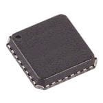
| 描述 | IC OPAMP INSTR 32LFCSP仪表放大器 Industrial I/V Outpt Driver +60V IC |
| DevelopmentKit | EVAL-CN0204-SDPZ |
| 产品分类 | Linear - Amplifiers - Instrumentation, OP Amps, Buffer Amps集成电路 - IC |
| 品牌 | Analog Devices |
| 产品手册 | |
| 产品图片 |
|
| rohs | 符合RoHS无铅 / 符合限制有害物质指令(RoHS)规范要求 |
| 产品系列 | 放大器 IC,仪表放大器,Analog Devices AD5751BCPZ- |
| 数据手册 | |
| 产品型号 | AD5751BCPZ |
| 产品培训模块 | http://www.digikey.cn/PTM/IndividualPTM.page?site=cn&lang=zhs&ptm=30008http://www.digikey.cn/PTM/IndividualPTM.page?site=cn&lang=zhs&ptm=26202 |
| 产品目录页面 | |
| 产品种类 | 仪表放大器 |
| 供应商器件封装 | 32-LFCSP-VQ(5x5) |
| 包装 | 托盘 |
| 压摆率 | 2 V/µs |
| 商标 | Analog Devices |
| 增益带宽积 | - |
| 安装类型 | 表面贴装 |
| 安装风格 | SMD/SMT |
| 封装 | Tray |
| 封装/外壳 | 32-VFQFN 裸露焊盘,CSP |
| 封装/箱体 | LFCSP-32 |
| 工作温度 | -40°C ~ 105°C |
| 工作温度范围 | - 40 C to + 105 C |
| 工作电源电压 | 10.8 V to 55 V |
| 工厂包装数量 | 490 |
| 放大器类型 | 仪表 |
| 最大功率耗散 | 108 mW |
| 最大工作温度 | + 105 C |
| 最小工作温度 | - 40 C |
| 标准包装 | 1 |
| 电压-电源,单/双 (±) | 10.8 V ~ 55 V |
| 电压-输入失调 | - |
| 电流-电源 | 5.2mA |
| 电流-输入偏置 | - |
| 电流-输出/通道 | 24mA |
| 电源电流 | 4.4 mA |
| 电路数 | 1 |
| 系列 | AD5751 |
| 视频文件 | http://www.digikey.cn/classic/video.aspx?PlayerID=1364138032001&width=640&height=505&videoID=2245193153001http://www.digikey.cn/classic/video.aspx?PlayerID=1364138032001&width=640&height=505&videoID=2245193159001 |
| 转换速度 | 2 V/us |
| 输出类型 | - |
| 通道数量 | 1 Channel |


- 商务部:美国ITC正式对集成电路等产品启动337调查
- 曝三星4nm工艺存在良率问题 高通将骁龙8 Gen1或转产台积电
- 太阳诱电将投资9.5亿元在常州建新厂生产MLCC 预计2023年完工
- 英特尔发布欧洲新工厂建设计划 深化IDM 2.0 战略
- 台积电先进制程称霸业界 有大客户加持明年业绩稳了
- 达到5530亿美元!SIA预计今年全球半导体销售额将创下新高
- 英特尔拟将自动驾驶子公司Mobileye上市 估值或超500亿美元
- 三星加码芯片和SET,合并消费电子和移动部门,撤换高东真等 CEO
- 三星电子宣布重大人事变动 还合并消费电子和移动部门
- 海关总署:前11个月进口集成电路产品价值2.52万亿元 增长14.8%


PDF Datasheet 数据手册内容提取
Industrial I/V Output Driver, Single-Supply, 55 V Maximum Supply, Programmable Ranges Data Sheet AD5751 FEATURES GENERAL DESCRIPTION Current output ranges: 0 mA to 20 mA, 0 mA to 24 mA, The AD5751 is a single-channel, low cost, precision, voltage/ or 4 mA to 20 mA current output driver with hardware or software programmable ±0.03% FSR typical total unadjusted error (TUE) output ranges. The software ranges are configured via an SPI-/ ±5 ppm/°C typical output drift MICROWIRE™-compatible serial interface. The AD5751 targets 2% overrange applications in PLC and industrial process control. The analog Voltage output ranges: 0 V to 5 V, 0 V to 10 V, 0 V to 40 V input to the AD5751 is provided from a low voltage, single-supply ±0.02% FSR typical total unadjusted error (TUE) digital-to-analog converter (DAC) and is internally conditioned ±3 ppm/°C typical output drift to provide the desired output current/voltage range. Overrange capability on all ranges The output current range is programmable across three current Flexible serial digital interface ranges: 0 mA to 20 mA, 0 mA to 24 mA, or 4 mA to 20 mA. On-chip output fault detection PEC error checking Voltage output is provided from a separate pin that can be Asynchronous CLEAR function configured to provide 0 V to 5 V, 0 V to 10 V, and 0 V to 40 V Power supply range output ranges. An overrange is available on the voltage ranges. AVDD: 12 V (± 10%) to 55 V (maximum) Analog outputs are short-circuit and open-circuit protected and Output loop compliance to AVDD − 2.75 V can drive capacitive loads of 1 μF and inductive loads of 0.1 H. Temperature range: −40°C to +105°C The device is specified to operate with a power supply range from 32-lead 5 mm × 5 mm LFCSP package 10.8 V to 55 V. Output loop compliance is 0 V to AV − 2.75 V. DD APPLICATIONS The flexible serial interface is SPI and MICROWIRE compatible Process control and can be operated in 3-wire mode to minimize the digital Actuator control isolation required in isolated applications. The interface also PLCs features an optional PEC error checking feature using CRC-8 error checking, useful in industrial environments where data communication corruption can occur. The device also includes a power-on reset function ensuring that the device powers up in a known state (0 V or tristate) and an asynchronous CLEAR pin that sets the outputs to zero- scale/midscale voltage output or the low end of the selected current range. An HW SELECT pin is used to configure the part for hardware or software mode on power-up. Table 1. Related Device Part Number Description AD5422 Single-channel, 16-bit, serial input current source and voltage output DAC Rev. D Document Feedback Information furnished by Analog Devices is believed to be accurate and reliable. However, no responsibility is assumed by Analog Devices for its use, nor for any infringements of patents or other One Technology Way, P.O. Box 9106, Norwood, MA 02062-9106, U.S.A. rights of third parties that may result from its use. Specifications subject to change without notice. No license is granted by implication or otherwise under any patent or patent rights of Analog Devices. Tel: 781.329.4700 ©2009–2018 Analog Devices, Inc. All rights reserved. Trademarks and registered trademarks are the property of their respective owners. Technical Support www.analog.com
AD5751 Data Sheet TABLE OF CONTENTS Features .............................................................................................. 1 OUTEN ........................................................................................ 24 Applications ....................................................................................... 1 Software Control ........................................................................ 24 General Description ......................................................................... 1 Hardware Control ...................................................................... 26 Revision History ............................................................................... 2 Transfer Function ....................................................................... 26 Functional Block Diagram .............................................................. 3 Detailed Description of Features .................................................. 27 Specifications ..................................................................................... 4 Output Fault Alert—Software Mode ....................................... 27 Timing Characteristics ................................................................ 7 Output Fault Alert—Hardware Mode ..................................... 27 Absolute Maximum Ratings ............................................................ 9 Voltage Output Short-Circuit Protection ................................ 27 ESD Caution .................................................................................. 9 Asynchronous Clear (CLEAR) ................................................. 27 Pin Configuration and Function Descriptions ........................... 10 External Current Setting Resistor ............................................ 27 Typical Performance Characteristics ........................................... 12 Programmable Overrange Modes ............................................ 28 Current Output ........................................................................... 15 Packet Error Checking ............................................................... 28 Terminology .................................................................................... 20 Applications Information .............................................................. 29 Theory of Operation ...................................................................... 21 Transient Voltage Protection .................................................... 29 Software Mode ............................................................................ 21 Thermal Considerations ............................................................ 29 Currrent Output Architecture .................................................. 23 Layout Guidelines....................................................................... 30 Driving Inductive Loads ............................................................ 23 Galvanically Isolated Interface ................................................. 30 Power-On State of the AD5751 ................................................ 23 Microprocessor Interfacing ....................................................... 30 Default Registers at Power-On ................................................. 24 Outline Dimensions ....................................................................... 31 Reset Function ............................................................................ 24 Ordering Guide .......................................................................... 31 REVISION HISTORY 1/2018—Rev. C to Rev. D 10/2013—Rev. A to Rev. B Changed CP-32-7 to CP-32-2 ...................................... Throughout Changed Thermal Impedance from 28°C/W to 42°C/W Changes to Figure 4 ........................................................................ 10 (Throughout) ..................................................................................... 9 Updated Outline Dimensions ....................................................... 31 Added Endnote 1 to Table 4 ............................................................. 9 Changes to Ordering Guide .......................................................... 31 Changes to Table 12 Calculations................................................. 29 Updated Outline Dimensions ....................................................... 31 3/2017—Rev. B to Rev. C Changed CP-32-2 to CP-32-7 ...................................... Throughout 5/2010—Rev. 0 to Rev. A Changes to Figure 4 ........................................................................ 10 Changes to Table 2, Power Requirements ...................................... 6 Updated Outline Dimensions ....................................................... 31 Changes to Ordering Guide .......................................................... 31 10/2009—Revision 0: Initial Version Rev. D | Page 2 of 32
Data Sheet AD5751 FUNCTIONAL BLOCK DIAGRAM DVCC GND AVDD GND COMP1COMP2 CLEAR CLRSEL VSENSE+ SCLK/OUTEN* INPUTSHIFT REGISTER SDIN/R0* VOUTRANGE AND VOUT SYNC/RSET* CONTROL SCALING SDO/VFAULT* LOGIC VOUT SHORTFAULT HWSELECT STATUS REGISTER AVDD VIN VREF R2 R3 RESET IOUTRANGE SCALING IOUT OVERTEMP REXT1 FAULT/TEMP* VOUTSHORTFAULT RSET REXT2 NC/IFAULT* IOUT OPENFAULT POWER- IOUT AD5751 ONRESET OPENFAULT AD2/R1* AD1/R2* AD0/R3* *DDPIEENNNTOOATTKEEESDSSB OHYNAITRFAEALDUICLPTITNEF.UXSTNO.CFFTTOIWORNAE.R XIENAMMHOAPRLDEDE,WDFAEORNROEFTMAEOUDLDBTEY/,TTERHMEIGSPUPPLIINNA,RT IANTKESEXOSTF ,OTHWNAATRREDEMWPMAOFRUEDNEMC,OTTDHIOEISN. 07269-001 Figure 1. Functional Block Diagram Rev. D | Page 3 of 32
AD5751 Data Sheet SPECIFICATIONS AV = 12 V (± 10%) to 55 V (maximum), DV = 2.7 V to 5.5 V, GND = 0 V. IOUT: R = 300 Ω. All specifications T to T , DD CC LOAD MIN MAX unless otherwise noted. Table 2. Parameter1 Min Typ Max Unit Test Conditions/Comments INPUT VOLTAGE RANGE Output unloaded 0 to 4.096 V Input Leakage Current −1 +1 µA REFERENCE INPUT Reference Input Voltage 4.096 V External reference must be exactly as stated; otherwise, accuracy errors show up as error in output Input Leakage Current −1 +1 µA VOLTAGE OUTPUT Output Voltage Ranges 0 5 V 0 10 V AVDD must have minimum 1.3 V headroom or >11.3 V 0 40 V Output Voltage Overranges2 0 6 V Programmable overranges; see Detailed Description of Features section 0 12 V 0 44 V Accuracy Total Unadjusted Error (TUE) B Version3 −0.1 +0.1 % FSR −0.05 ±0.02 +0.05 % FSR T = 25°C A A Version3 −0.3 +0.3 % FSR −0.1 ±0.05 +0.1 % FSR T = 25°C A Relative Accuracy (INL) −0.02 ±0.005 +0.02 % FSR Dead Band on Output, RTI −14 8 +14 mV Referred to 4.096 V input range Offset Error −5 +5 mV 0 V to 10 V range −4 ±0.5 +4 mV T = 25°C, 0 V to 10 V range A −3 +3 mV 0 V to 5 V range −2.2 ±0.3 +2.2 mV T = 25°C, 0 V to 5 V range A −20 +20 mV 0 V to 40 V range −17 ±0.5 +17 mV T = 25°C, 0 V to 40 V range A Gain Error −0.05 +0.05 % FSR 0 V to 5 V, 0 V to 10 V range −0.04 ±0.015 +0.04 % FSR T = 25°C A −0.09 +0.09 % FSR 0 V to 40 V range −0.05 ±0.02 +0.05 % FSR T = 25°C A Gain Error TC4 ±0.5 ppm FSR/°C All ranges Full-Scale Error −0.05 +0.05 % FSR 0 V to 5 V, 0 V to 10 V range −0.04 ±0.015 +0.04 % FSR T = 25°C A −0.09 +0.09 % FSR 0 V to 40 V range −0.05 ±0.02 +0.05 % FSR T = 25°C A Full-Scale Error TC4 ±1.5 ppm FSR/°C All ranges OUTPUT CHARACTERISTICS4 Headroom 1.3 V Output unloaded Short-Circuit Current 15 mA Load 1 kΩ For specified performance, 0 V to 5 V and 0 V to 10 V ranges 5 kΩ For specified performance, 0 V to 40 V range Rev. D | Page 4 of 32
Data Sheet AD5751 Parameter1 Min Typ Max Unit Test Conditions/Comments Capacitive Load Stability T = 25°C A R = ∞ 1 nF LOAD R = 1 kΩ 1 nF LOAD R = ∞ 2 µF External compensation capacitor required; LOAD see Driving Large Capacitive Loads section DC Output Impedance 0.12 Ω Settling Time 0 V to 5 V Range, ¼ to ¾ Step 7 µs Specified with 2 kΩ || 220 pF, ±0.05% 0 V to 5 V Range, 40 mV Input Step 4.5 µs Specified with 2 kΩ || 220 pF, ±0.05% 0 V to 40 V Range, ¼ to ¾ Step 15.8 µs Specified with 5 kΩ || 220 pF, ±0.05% Slew Rate 2 V/µs Specified with 1 kΩ || 220 pF Output Noise 3.5 µV rms 0.1 Hz to 10 Hz bandwidth 45.5 µV rms 100 kHz bandwidth; specified with 2 kΩ || 220 pF Output Noise Spectral Density 165 nV/√Hz Measured at 10 kHz; specified with 2 kΩ || 220 pF AC PSRR 65 dB 200 mV, 50 Hz/60 Hz sine wave superimposed on power supply voltage DC PSRR 10 µV/V CURRENT OUTPUT Output Current Ranges 0 24 mA 0 20 mA 3.92 20 mA Output Current Overranges2 0 24.5 mA See Detailed Description of Features section 0 20.4 mA See Detailed Description of Features section 3.92 20.4 mA See Detailed Description of Features section ACCURACY (INTERNAL R ) SET Total Unadjusted Error (TUE) B Version3 −0.2 +0.2 % FSR −0.08 ±0.03 +0.08 % FSR T = 25°C A A Version3 −0.5 +0.5 % FSR −0.3 ±0.15 +0.3 % FSR T = 25°C A Relative Accuracy (INL) −0.02 ±0.01 +0.02 % FSR Offset Error −16 +16 µa −10 +5 +10 µa T = 25°C A Offset Error TC4 ±3 ppm FSR/°C Dead Band on Output, RTI 8 +14 mV Referred to 4.096 V input range Gain Error −0.2 +0.2 % FSR −0.125 ±0.02 +0.125 % FSR T = 25°C A Gain TC4 ±10 ppm FSR/°C Full-Scale Error −0.2 +0.2 % FSR −0.125 ±0.02 +0.125 % FSR T = 25°C A Full-Scale TC4 ±4 ppm FSR/°C ACCURACY (EXTERNAL R ) SET Total Unadjusted Error (TUE) B Version3 −0.1 +0.1 % FSR −0.08 ±0.03 +0.08 % FSR T = 25°C A A Version3 −0.3 +0.3 % FSR −0.1 ±0.02 +0.1 % FSR T = 25°C A Relative Accuracy (INL) −0.02 ±0.01 +0.02 % FSR Offset Error −14 +14 µA −11 +5 +11 T = 25°C A Offset Error TC4 ±2 ppm FSR/°C Dead Band on Output, RTI 8 +14 mV Referred to 4.096 V input range Gain Error −0.08 +0.08 % FSR −0.07 ±0.02 +0.07 % FSR T = 25°C A Rev. D | Page 5 of 32
AD5751 Data Sheet Parameter1 Min Typ Max Unit Test Conditions/Comments Gain TC4 ±1 ppm FSR/°C Full-Scale Error −0.1 +0.1 % FSR −0.07 ±0.02 +0.07 % FSR T = 25°C A Full-Scale TC4 ±2 ppm FSR/°C OUTPUT CHARACTERISTICS4 Current Loop Compliance Voltage 0 AV − 2.75 V DD Resistive Load Chosen such that compliance is not exceeded Inductive Load See test conditions/comments column H Needs appropriate capacitor at higher inductance values; see Driving Inductive Loads section Settling Time 4 mA to 20 mA, Full-Scale Step 8.5 µs 250 Ω load 120 µA Step, 4 mA to 20 mA Range 1.2 µs 250 Ω load DC PSRR 1 µA/V Output Impedance 130 MΩ DIGITAL INPUTS4 JEDEC compliant Input High Voltage, V 2 V IH Input Low Voltage, V 0.8 V IL Input Current −1 +1 µA Per pin Pin Capacitance 5 pF Per pin DIGITAL OUTPUTS4 FAULT, IFAULT, TEMP, VFAULT V , Output Low Voltage 0.4 V 10 kΩ pull-up resistor to DVCC OL 0.6 V At 2.5 mA V , Output High Voltage 3.6 V 10 kΩ pull-up resistor to DVCC OH SDO V , Output Low Voltage 0.5 0.5 V Sinking 200 µA OL V , Output High Voltage DVCC − 0.5 DVCC − 0.5 V Sourcing 200 µA OH High Impedance Output 3 pF Capacitance High Impedance Leakage Current −1 +1 µA POWER REQUIREMENTS AV 10.8 55 V DD DV CC Input Voltage 2.7 5.5 V AI 4.4 5.6 mA Output unloaded, output disabled DD 5.2 6.2 mA Current output enabled 5.2 6.2 mA Voltage output enabled DI 0.3 1 mA V = DVCC, V = GND CC IH IL Power Dissipation 108 mW AVDD = 24 V, outputs unloaded 1 Temperature range: −40°C to +105°C; typical at +25°C. 2 Overranges are nominal; gain and offset are not trimmed as per nominal ranges. 3 Specification includes gain and offset errors, over temperature, and drift after 1000 hours, TA = 125°C. 4 Guaranteed by characterization, but not production tested. Rev. D | Page 6 of 32
Data Sheet AD5751 TIMING CHARACTERISTICS AV = 12 V (± 10%) to 55 V (maximum), DV = 2.7 V to 5.5 V, GND = 0 V. VOUT: R = 2 kΩ (5 kΩ for 0 V to 40 V range), DD CC LOAD C = 200 pF, IOUT: R = 300 Ω. All specifications T to T , unless otherwise noted. L LOAD MIN MAX Table 3. Parameter1, 2 Limit at T , T Unit Description MIN MAX t 20 ns min SCLK cycle time 1 t 8 ns min SCLK high time 2 t 8 ns min SCLK low time 3 t4 5 ns min SYNC falling edge to SCLK falling edge setup time t5 10 ns min 16th SCLK falling edge to SYNC rising edge (on 24th SCLK falling edge if using PEC) t6 5 ns min Minimum SYNC high time (write mode) t 5 ns min Data setup time 7 t 5 ns min Data hold time 8 t, t 1.5 µs max CLEAR pulse low/high activation time 9 10 t11 5 ns min Minimum SYNC high time (read mode) t 40 ns max SCLK rising edge to SDO valid (SDO C = 15 pF) 12 L t13 10 ns min RESET pulse low time 1 Guaranteed by characterization, but not production tested. 2 All input signals are specified with tR = tF = 5 ns (10% to 90% of DVCC) and timed from a voltage level of 1.2 V. Timing Diagrams t1 SCLK 1 2 16 t6 t3 t2 t4 t5 SYNC t8 t7 SDIN D15 D0 CLEAR t10 t9 VOUT RESET t13 07269-003 Figure 2. Write Mode Timing Diagram Rev. D | Page 7 of 32
AD5751 Data Sheet SCLK SYNC t11 SDIN A2 A1 A0 R = 1 0 X X X X X X X X X X X t12 SDO X X X X X R3 R2 R1 R0 CLRSEL OUTEN RSET ERPREOCR OTEVMERP FIAOUULTT FVAOUULTT 07269-004 Figure 3. Readback Mode Timing Diagram Rev. D | Page 8 of 32
Data Sheet AD5751 ABSOLUTE MAXIMUM RATINGS T = 25°C, unless otherwise noted. Transient currents of up to Stresses at or above those listed under Absolute Maximum A 100 mA do not cause SCR latch-up. Ratings may cause permanent damage to the product. This is a stress rating only; functional operation of the product at these Table 4. or any other conditions above those indicated in the operational Parameter Rating section of this specification is not implied. Operation beyond AVDD to GND −0.3 V to +58 V the maximum operating conditions for extended periods may DVCC to GND −0.3 V to +7 V affect product reliability. Digital Inputs to GND −0.3 V to DV + 0.3 V, or 7 V CC ESD CAUTION (whichever is less) Digital Outputs to GND −0.3 V to DV + 0.3 V, or 7 V CC (whichever is less) VREF to GND −0.3 V to +7 V VSENSE+ to GND −0.3 V to AV DD VIN to GND −0.3 V to +7 V VOUT, IOUT to GND −0.3 V to AV DD Operating Temperature Range Industrial −40°C to +105°C Storage Temperature Range −65°C to +150°C Junction Temperature (T max) 125°C J 32-Lead LFCSP Package θ Thermal Impedance1 42°C/W JA Lead Temperature JEDEC industry standard Soldering J-STD-020 1 Simulated data based on a JEDEC 2s2p test board with thermal vias. Rev. D | Page 9 of 32
AD5751 Data Sheet PIN CONFIGURATION AND FUNCTION DESCRIPTIONS AULTT/TEMPTELECT FLES C/IAUESWCCCC NFRHNNNN 21098765 33322222 SDO/VFAULT 1 24 VSENSE+ CLRSEL 2 23 VOUT CLEAR 3 AD5751 22 GND DVCC 4 21 GND TOPVIEW GND 5 (NottoScale) 20 COMP1 SYNC/RSET 6 19 COMP2 SCLK/OUTEN 7 18 IOUT SDIN/R0 8 17 AVDD 90123456 1111111 12321FND AD2/RAD1/RAD0/RREXTREXTVREVIGN N12..ONTTHCEES=ENXOPOCSOENDNEPCATD.D CLAEN I SBET ITEIDEDT OT OG NGDN.D. 07269-005 Figure 4. Pin Configuration Table 5. Pin Function Descriptions Pin No. Mnemonic Description 1 SDO/VFAULT Serial Data Output (SDO). In software mode, this pin is used to clock data from the input shift register in readback mode. Data is clocked out on the rising edge of SCLK and is valid on the falling edge of SCLK. This pin is a CMOS output. Short-Circuit Fault Alert (VFAULT). In hardware mode, this pin acts as a short-circuit fault alert pin and is asserted low when a short-circuit error is detected. This pin is an open-drain output and must be connected to a pull-up resistor. 2 CLRSEL In hardware or software mode, this pin selects the clear value, either zero-scale or midscale code. In software mode, this pin is implemented as a logic OR with the internal CLRSEL bit. 3 CLEAR Active High Input. Asserting this pin sets the output current/voltage to zero-scale code or midscale code of range selected (user-selectable). CLEAR is a logic OR with the internal clear bit. See the Asynchronous Clear (CLEAR) section for more details. In software mode, during power-up, the CLEAR pin level determines the power-on condition of the voltage channel, which can be active 0 V or tristate. 4 DVCC Digital Power Supply. 5 GND Ground Connection. 6 SYNC/RSET Positive Edge-Sensitive Latch (SYNC). In software mode, a rising edge parallel loads the input shift register data into the AD5751, also updating the output. Resistor Select (RSET). In hardware mode, this pin selects whether the internal or the external current sense resistor is used. If RSET = 0, the external sense resistor is chosen. If RSET = 1, the internal sense resistor is chosen. 7 SCLK/OUTEN Serial Clock Input (SCLK). In software mode, data is clocked into the input shift register on the falling edge of SCLK. This pin operates at clock speeds up to 50 MHz. Output Enable (OUTEN). In hardware mode, this pin acts as an output enable pin. 8 SDIN/R0 Serial Data Input (SDIN). In software mode, data must be valid on the falling edge of SCLK. Range Decode Bit (R0). In hardware mode, this pin, in conjunction with R1, R2, and R3, selects the output current/voltage range setting on the part. 9 AD2/R1 Device Addressing Bit (AD2). In software mode, this pin, in conjunction with AD0 and AD1, allows up to eight devices to be addressed on one bus. Range Decode Bit (R1). In hardware mode, this pin, in conjunction with R0, R2, and R3, selects the output current/voltage range setting on the part. Rev. D | Page 10 of 32
Data Sheet AD5751 Pin No. Mnemonic Description 10 AD1/R2 Device Addressing Bit (AD1). In software mode, this pin, in conjunction with AD0 and AD2, allows up to eight devices to be addressed on one bus. Range Decode Bit (R2). In hardware mode, this pin, in conjunction with R0, R1, and R3, selects the output current/voltage range setting on the part. 11 AD0/R3 Device Addressing Bit (AD0). In software mode, this pin, in conjunction with AD1 and AD2, allows up to eight devices to be addressed on one bus. Range Decode Bit (R3). In hardware mode, this pin, in conjunction with R0, R1, and R2, selects the output current/voltage range setting on the part. 12, 13 REXT2, REXT1 A 15 kΩ external current setting resistor can be connected between the REXT1 and REXT2 pins to improve the IOUT temperature drift performance. 14 VREF Buffered Reference Input. 15 VIN Buffered Analog Input (0 V to 4.096 V). 16 GND Ground Connection. 17 AVDD Positive Analog Supply. 18 IOUT Current Output. 19, 20 COMP2, COMP1 Optional Compensation Capacitor Connections for the Voltage Output Buffer. These are used to drive higher capacitive loads on the output. These pins also reduce overshoot on the output. Care should be taken when choosing the value of the capacitor connected between the COMP1 and COMP2 pins because it has a direct influence on the settling time of the output. See the Driving Large Capacitive Loads section for further details. 21 GND Ground Connection. 22 GND Ground Connection. 23 VOUT Buffered Analog Output Voltage. 24 VSENSE+ Sense Connection for the Positive Voltage Output Load Connection. 25, 26, 27, 28 NC No Connect. Can be tied to GND. 29 HW SELECT This part is used to configure the part to hardware or software mode. HW SELECT = 0 selects software control. HW SELECT = 1 selects hardware control. 30 RESET In software mode, this pin resets the part to its power-on state. Active low. In hardware mode, there is no reset. If using the part in hardware mode, the RESET pin should be tied high. 31 FAULT/TEMP Fault Alert (FAULT). In software mode, this pin acts as a general fault alert pin. It is asserted low when an open-circuit, short-circuit, overtemperature error, or PEC interface error is detected. This pin is an open- drain output and must be connected to a pull-up resistor. Overtemperature Fault (TEMP). In hardware mode, this pin acts as an overtemperature fault pin. It is asserted low when an overtemperature error is detected. This pin is an open-drain output and must be connected to a pull-up resistor. 32 NC/IFAULT No Connect (NC). In software mode, this pin is a no connect. Instead, tie this pin to GND. Open-Circuit Fault Alert (IFAULT). In hardware mode, this pin acts as an open-circuit fault alert pin. It is asserted low when an open-circuit error is detected. This pin is an open-drain output and must be connected to a pull-up resistor. 33 (EPAD) Exposed paddle The exposed paddle is tied to GND. Rev. D | Page 11 of 32
AD5751 Data Sheet TYPICAL PERFORMANCE CHARACTERISTICS 0.010 0.10 0VTO5V 0VTO5VPOSITIVETUE R (%FSR) 00..000086 00VVTTOO1400VV DJUSTED 00..0086 0000VVVVTTTTOOOO154100V0VVVNNPPEOOEGGSSAIIATTTTIIIVVVIVEEEETTTTUUUUEEEE RO 0.004 NA 0.04 0VTO40VNEGATIVETUE R U E L R) Y 0.002 AS 0.02 NEARIT 0 VE TOTOR (%F 0 ONLI–0.002 GATIERR–0.02 AL N–0.004 E/NE –0.04 GR–0.006 TIV –0.06 E SI INT–0.008 PO –0.08 –0.010 0.020 0.293 0.585 0.878 1.170 1.463 1.755VIN2.048(V)2.341 2.633 2.926 3.218 3.511 3.803 4.096 07269-014 –0.10 –40 TEMPERA2T5URE(°C) 105 07269-017 Figure 5. Integral Nonlinearity Error vs. VIN Figure 8. Total Unadjusted Error vs. Temperature 0.010 0.05 0VTO5VRANGE 0VTO5VRANGE FSR) 0.008 00VVTTOO1400VVRRAANNGGEE 0.04 00VVTTOO1400VVRRAANNGGEE R (% 0.006 R) 0.03 O S RR 0.004 %F 0.02 RITY E 0.002 RROR ( 0.01 A 0 E LINE–0.002 ALE 0 N C AL NO–0.004 ULL-S–0.01 GR–0.006 F–0.02 E NT–0.008 –0.03 I –0.010 –40 TEMPERA2T5URE(°C) 105 07269-015 –0.04 –40 TEMPERA2T5URE(°C) 105 07269-018 Figure 6. Integral Nonlinearity Error vs. Temperature Figure 9. Full-Scale Error vs. Temperature 0.04 0.010 0VTO5V 0VTO5VRANGE 0.008 0VTO10V 0.03 0VTO10VRANGE R) 0VTO40V 0VTO40VRANGE S %F 0.006 0.02 R ( 0.004 R) O S ADJUSTED ERR–00..0000220 AIN ERROR (%F–00..00110 N G L U–0.004 –0.02 A T–0.006 TO –0.03 –0.008 –0.010 0.020 0.293 0.585 0.878 1.170 1.463 1.755VIN2.048(V)2.341 2.633 2.926 3.218 3.511 3.803 4.096 07269-016 –0.04 –40 TEMPERA2T5URE(°C) 105 07269-019 Figure 7. Total Unadjusted Error vs. VIN Figure 10. Gain Error vs. Temperature Rev. D | Page 12 of 32
Data Sheet AD5751 4.0 1.00 0VTO5VRANGE VDD HEADROOM, LOAD OFF 3.5 0VTO10VRANGE 0VTO40VRANGE 0.95 3.0 V) 2.5 m 0.90 OR ( 2.0 M (V) R 1.5 O T ER 1.0 DRO0.85 E A S E F 0.5 H F 0.80 O 0 –0.5 0.75 –1.0 –1.5 –40 TEMPERA2T5URE(°C) 105 07269-020 0.70 –40 TEMPERA2T5URE (°C) 105 07269-023 Figure 11. Offset Error vs. Temperature Figure 14. AVDD Headroom, 0 V to 10 V Range, Output Set to 10 V, Load Off 0.010 0.007 5VLINEARITY,NOLOAD 5V RANGE FSR) 0.008 1400VVLLIINNEEAARRIITTYY,,NNOOLLOOAADD 0.006 OR (% 0.006 A (V) 0.005 R 0.004 T R L 0.004 LINEARITY E–00..0000220 VOLTAGE DE 00..000032 L NON–0.004 TPUT 0.001 GRA–0.006 OU 0 E NT–0.008 –0.001 I –0.010 24 SUPPLYV4O8LTAGE(V) 55 07269-021 –0.002–15–13–11 –9 S–7OU–R5CE–/3SIN–K1 CU1RR3ENT5 (mA7) 9 11 13 15 07269-024 Figure 12. INL Error vs. Supply Voltage Figure 15. Source and Sink Capability of Output Amplifier 0.010 12 0.008 SR) 10 F 0.006 % R ( 0.004 O 8 D ERR 0.002 000VVV TTTOOO 514V00VV P PPOOOSSSITIITTIVIIVVEEE T TTUUUEEE GE (V) DJUSTE–0.0020 00VV TTOO 51V0V N NEEGGAATTIVIVEE T TUUEE VOLTA 6 NA 0V TO 40V NEGATIVE TUE 4 U–0.004 L A OT–0.006 2 T –0.008 –0.010 24 SUPPLY V4O8LTAGE (V) 55 07269-022 0–8 –3 2 7 TIM1E2 (µs) 17 22 27 07269-025 Figure 13. Total Unadjusted Error vs. Supply Voltage Figure 16. Full-Scale Positive Step, 10 V Range Rev. D | Page 13 of 32
AD5751 Data Sheet 12 10 8 V) E ( G A 6 T L O V 4 2 0–8 –3 2 7 TIM1E2 (µs) 17 22 27 07269-026 5µV/DIV 1s/DIV 07269-029 Figure 17. Full-Scale Negative Step, 10 V Range Figure 20. Peak-to-Peak Noise (0.1 Hz to 10 Hz Bandwidth) 40 35 30 25 mV) 20 (OUT15 V 10 5 –50–1.0 –0.5 0 0T.5IME (m1s.)0 1.5 2.0 2.5 07269-027 100µV/DIV 1s/DIV 07269-030 Figure 18. VOUT vs. Time on Power-Up, Load = 2 kΩ || 200 pF Figure 21. Peak-to-Peak Noise (100 kHz Bandwidth) 4.0 1.0 3.5 0.8 3.0 1 VDD 0.6 2.5 (V)VDD2.0 0.4 V (V)OUT 1.5 0.2 1.0 VOUT 2 0 0.5 0 –0.2 CH1 5.00V CH2 20.0mV BWM1.0µs A CH1 3.00V07269-028 –1.5 –1.0 –0.5 0TIME (m0s.)5 1.0 1.5 2.0 07269-031 Figure 19. VOUT Enable Glitch, Load = 2 kΩ || 1 nF Figure 22. VDD and VOUT vs. Time on Power-Up Rev. D | Page 14 of 32
Data Sheet AD5751 CURRENT OUTPUT 0.005 0.010 4mATO20mAEXTERNALRSETRESISTOR 4mATO20mA INTERNALRSETLINEARITY 0.004 0mATO20mAEXTERNALRSETRESISTOR 0.008 0mATO20mA INTERNALRSETLINEARITY R) 0mATO24mAEXTERNALRSETRESISTOR R) 0mATO24mA INTERNALRSETLINEARITY S 0.003 S 0.006 F F % % Y ( 0.002 Y ( 0.004 T T ARI 0.001 ARI 0.002 E E N N LI 0 LI 0 N N O O N–0.001 N–0.002 L L A A R–0.002 R–0.004 G G E E NT–0.003 NT–0.006 I I –0.004 –0.008 –0.005 0.020 0.293 0.585 0.878 1.170 1.463 1.755VIN2.048(V) 2.341 2.633 2.926 3.218 3.511 3.803 4.096 07269-032 –0.010 24V SUPPLYVO4L8TVAGE(AVDD) 55V 07269-035 Figure 23. Integral Nonlinearity Error vs. VIN, External RSET Resistor Figure 26. Integral Nonlinearity Current Mode, Internal RSET Sense Resistor 0.005 0.05 4mATO20mA INTERNALRSETRESISTOR 4mATO20mAEXTERNALRSETTUE R) 0.004 00mmAATTOO2204mmAA IINNTTEERRNNAALLRRSSEETTRREESSIISSTTOORR SR) 0.04 00mmAATTOO2204mmAAEEXXTTEERRNNAALLRRSSEETTTTUUEE FS 0.003 %F 0.03 Y (% 0.002 OR ( 0.02 T R ARI 0.001 ER 0.01 E D N E NONLI–0.0010 DJUST–0.010 L A A N R–0.002 U–0.02 EG AL NT–0.003 OT–0.03 I T –0.004 –0.04 –0.005 0.020 0.293 0.585 0.878 1.170 1.463 1.755VIN2.048(V)2.341 2.633 2.926 3.218 3.511 3.803 4.096 07269-033 –0.05 0.020 0.293 0.585 0.878 1.170 1.463 1.755VIN2.048(V)2.341 2.633 2.926 3.218 3.511 3.803 4.096 07269-036 Figure 24. Integral Nonlinearity Error vs. VIN, Internal RSET Resistor Figure 27. Total Unadjusted Error vs. VIN, External RSET Resistor 0.010 0.05 4mATO20mAEXTERNALRSETLINEARITY 4mATO20mA INTERNALRSETTUE R) 0.008 00mmAATTOO2204mmAAEEXXTTEERRNNAALLRRSSEETTLLIINNEEAARRIITTYY SR) 0.04 00mmAATTOO2204mmAA IINNTTEERRNNAALLRRSSEETTTTUUEE FS 0.006 %F 0.03 Y (% 0.004 OR ( 0.02 T R EARI 0.002 D ER 0.01 N E NONLI–0.0002 DJUST–0.010 L A A N GR–0.004 L U–0.02 E A NT–0.006 OT–0.03 I T –0.008 –0.04 –0.010 24V SUPPLYVO4L8TVAGE(AVDD) 55V 07269-034 –0.05 0.020 0.293 0.585 0.878 1.170 1.463 1.755VIN2.048(V)2.341 2.633 2.926 3.218 3.511 3.803 4.096 07269-037 Figure 25. Integral Nonlinearity Current Mode, External RSET Sense Resistor Figure 28. Total Unadjusted Error vs. VIN, Internal RSET Resistor Rev. D | Page 15 of 32
AD5751 Data Sheet 0.020 0.005 4mATO20mAEXTERNALRSETPOSITIVETUE 4mATO20mAEXTERNALRSETLINEARITY SR) 0.015 00mmAATTOO2204mmAAEEXXTTEERRNNAALLRRSSEETTPPOOSSIITTIIVVEETTUUEE R) 0.004 00mmAATTOO2204mmAAEEXXTTEERRNNAALLRRSSEETTLLIINNEEAARRIITTYY F S 0.003 OR (% 0.010 Y (%F 0.002 R T ER 0.005 ARI 0.001 STED 0 NLINE 0 U O ADJ–0.005 L N–0.001 N A U R–0.002 TOTAL ––00..001105 400mmmAAATTTOOO222004mmmAAAEEEXXXTTTEEERRRNNNAAALLLRRRSSSEEETTTNNNEEEGGGAAATTTIIIVVVEEETTTUUUEEE INTEG––00..000034 –0.020 24V SUPPLYVO4L8TVAGE(AVDD) 55V 07269-038 –0.005 –40 TEMPERA25TURE(°C) 105 07269-041 Figure 29. Total Unadjusted Error Current Mode, External RSET Sense Resistor Figure 32. Integral Nonlinearity Error vs. Temperature, External RSET Sense Resistor 0.010 4mATO20mA INTERNALRSETNEGATIVETUE 0.10 0mATO20mA INTERNALRSETNEGATIVETUE 4mA TO 20mA INTERNAL RSET POSITIVE TUE R) 0.005 0.08 0mA TO 20mA INTERNAL RSET POSITIVE TUE JUSTED ERROR (%FS––00..0001500 0R4RmmSSEEAATTTTNPOOOEGS2240IATmmTIVAAIVE EIINNTTTTUUEEEERRNNAALL GATIVE TUE (%FSR) 000...0006420 0400mmmmAAAA TTTTOOOO 22224004mmmmAAAA IIIINNNNTTTTEEEERRRRNNNNAAAALLLL RRRRSSSSEEEETTTT PNNNOEEEGGGSIAAATTTTIVIIIVVVEEEE T TTTUUUUEEEE AD NE–0.02 OTAL UN–0.015 OSITIVE/––00..0046 T–0.020 0mATO20mA INTERNALRSETPOSITIVETUE P 0mATO24mA INTERNALRSETPOSITIVETUE –0.08 –0.025 24V SUPPLYVO4L8TVAGE(AVDD) 55V 07269-039 –0.10 –40 TEMPERA2T5URE (°C) 105 07269-042 Figure 30. Total Unadjusted Error Current Mode, Internal RSET Sense Resistor Figure 33. Total Unadjusted Error vs. Temperature, Internal RSET Sense Resistor 0.005 0.10 4mATO20mA INTERNALRSETLINEARITY 0.004 0mATO20mA INTERNALRSETLINEARITY 0.08 %FSR) 0.003 0mATO24mA INTERNALRSETLINEARITY %FSR) 0.06 LINEARITY ( 00..0000210 ATIVE TUE ( 00..00420 N G NO–0.001 NE–0.02 L E/ INTEGRA––00..000023 POSITIV––00..0046 4004mmmmAAAA TTTTOOOO 22220040mmmmAAAA EEEEXXXXTTTTEEEERRRRNNNNAAAALLLL RRRRSSSSEEEETTTT PPPNOOOEGSSSIIIATTTTIIIVVVIVEEEE TTT TUUUUEEEE –0.004 –0.08 0mA TO 20mA EXTERNAL RSET NEGATIVE TUE 0mA TO 24mA EXTERNAL RSET NEGATIVE TUE –0.005 –40 TEMPERA25TURE(°C) 105 07269-040 –0.10 –40 TEMPERA2T5URE (°C) 105 07269-043 Figure 31. Integral Nonlinearity Error vs. Temperature, Figure 34. Total Unadjusted Error vs. Temperature, External RSET Sense Resistor Internal RSET Sense Resistor Rev. D | Page 16 of 32
Data Sheet AD5751 50 4 45 3 40 R (µA) 35 µA) 2 RRO 30 OR ( 1 O-SCALE E 2250 FFSET ERR 0 ER 15 O –1 Z 105 400mmmAAA TTTOOO 222004mmmAAA EEEXXXTTTEEERRRNNNAAALLL RRRSSSEEETTT –2 400mmmAAA TTTOOO 222004mmmAAA EEEXXXTTTEEERRRNNNAAALLL RRRSSSEEETTT 0 –40 TEMPERA2T5URE (°C) 105 07269-044 –3 –40 TEMPERA2T5URE (°C) 105 07269-047 Figure 35. Zero-Scale Error vs. Temperature, External RSET Sense Resistor Figure 38. Offset Error vs. Temperature, External RSET Sense Resistor 40 0.05 4mA TO 20mA EXTERNAL RSET 35 0.04 0mA TO 20mA EXTERNAL RSET 0mA TO 24mA EXTERNAL RSET 0.03 A) 30 SR) ROR (µ 25 OR (%F 00..0021 R R E R E 20 E 0 CAL ALE –0.01 O-S 15 SC R L-–0.02 E L Z 10 U 4mA TO 20mA INTERNAL RSET F–0.03 5 0mA TO 20mA INTERNAL RSET 0mA TO 24mA INTERNAL RSET –0.04 0 –40 TEMPERA2T5URE (°C) 105 07269-045 –0.05 –40 TEMPERA2T5URE (°C) 105 07269-048 Figure 36. Zero-Scale Error vs. Temperature, Internal RSET Sense Resistor Figure 39. Full-Scale Error vs. Temperature, External RSET Sense Resistor 3 0.10 4mA TO 20mA INTERNAL RSET 0.08 0mA TO 20mA INTERNAL RSET 2 0mA TO 24mA INTERNAL RSET 0.06 R) S OFFSET ERROR (µA) –110 L-SCALE ERROR (%F––0000....000024420 L U –2 4mA TO 20mA INTERNAL RSET F–0.06 0mA TO 20mA INTERNAL RSET –0.08 0mA TO 24mA INTERNAL RSET –3 –40 TEMPERA2T5URE (°C) 105 07269-046 –0.10 –40 TEMPERA2T5URE (°C) 105 07269-049 Figure 37. Offset Error vs. Temperature, Internal RSET Sense Resistor Figure 40. Full-Scale Error vs. Temperature, Internal RSET Sense Resistor Rev. D | Page 17 of 32
AD5751 Data Sheet 0.10 12 0.000010 4mA TO 20mA EXTERNAL RSET 0.08 0mA TO 20mA EXTERNAL RSET 0.000008 0mA TO 24mA EXTERNAL RSET 10 0.06 0.000006 R) 0.04 8 0.000004 S N ERROR (%F–00..00220 V (V)DD 64 IOUT –000.0.00000000022 I (A)OUT AI G–0.04 2 –0.000004 –0.06 –0.000006 0 –0.08 VDD –0.000008 –0.10 –40 TEMPERA2T5URE (°C) 105 07269-050 –2–10 –8 –6 –4 –2TIME0 (ms)2 4 6 8 10–0.000010 07269-053 Figure 41. Gain Error vs. Temperature, External RSET Sense Resistor Figure 44. Output Current vs. Time on VDD Power-Up 0.10 0 4mA TO 20mA INTERNAL RSET 0.08 0mA TO 20mA INTERNAL RSET –2 0mA TO 24mA INTERNAL RSET 0.06 –4 SR) 0.04 –6 F R (% 0.02 µA) –8 RRO 0 (OUT–10 N E–0.02 I AI –12 G–0.04 –14 –0.06 –0.08 –16 –0.10 –40 TEMPERA2T5URE (°C) 105 07269-051 –18–2 –1 0 1 2TIME3(µs)4 5 6 7 8 07269-054 Figure 42. Gain Error vs. Temperature, Internal RSET Sense Resistor Figure 45. Output Current vs. Time on Output Enable, 0 mA to 20 mA Range 2.10 0.025 2.05 0.020 2.00 NCE (V)11..9950 NT (A)0.015 A E PLI1.85 RR M U0.010 O C C1.80 1.75 0.005 AVDD COMPLIANCE VOLTAGE 1.70 1.65 –40 TEMPERA2T5URE (°C) 105 07269-052 0–12 –6 1 8 14 21TIM28E (µ3s4) 41 48 54 61 68 07269-055 Figure 43. Output Compliance vs. Temperature Figure 46. 4 mA to 20 mA Output Current Step Tested When IOUT = 10.8 mA, 0 mA to 24 mA Range Selected Rev. D | Page 18 of 32
Data Sheet AD5751 3000 4.10 2500 4.05 4.00 2000 A) DVCC = 5V A)3.95 DI (µCC1500 AI (mDD3.90 1000 3.85 500 3.80 DVCC = 3V 00 0.5 1.0 1.5 2L.O0GIC2 .L5EVE3.L0 (V)3.5 4.0 4.5 5.0 07269-056 3.75 24 AVD4D8(V) 55 07269-058 Figure 47. DICC vs. Logic Input Voltage Figure 49. AIDD vs. AVDD, IOUT = 0 mA 4.10 4.05 4.00 A) 3.95 (mD D AI 3.90 3.85 3.80 3.75 24 AVD4D8 (V) 55 07269-057 Figure 48. AIDD vs. AVDD, VOUT = 0 V Rev. D | Page 19 of 32
AD5751 Data Sheet TERMINOLOGY Total Unadjusted Error (TUE) Zero-Scale TC TUE is a measure of the output error taking all the various Zero-scale TC is a measure of the change in zero-scale error errors into account: INL error, offset error, gain error, and with a change in temperature. Zero-scale error TC is expressed output drift over supplies, temperature, and time. TUE is in ppm FSR/°C. expressed as a percentage of full-scale range (% FSR). Offset Error Relative Accuracy or Integral Nonlinearity (INL) Offset error is a measurement of the difference between the INL is a measure of the maximum deviation, in % FSR, from a actual VOUT and the ideal VOUT expressed in millivolts (mV) straight line passing through the endpoints of the output driver in the linear region of the transfer function. It can be negative transfer function. A typical INL vs. input voltage plot is shown or positive. in Figure 5. Output Voltage Settling Time Full-Scale Error Output voltage settling time is the amount of time it takes for Full-scale error is the deviation of the actual full-scale analog the output to settle to a specified level for a half-scale input change. output from the ideal full-scale output. Full-scale error is Slew Rate expressed as a percentage of full-scale range (% FSR). The slew rate of a device is a limitation in the rate of change of Full-Scale TC the output voltage. The output slewing speed is usually limited Full-scale TC is a measure of the change in the full-scale error by the slew rate of the amplifier used at its output. Slew rate is with a change in temperature. It is expressed in ppm FSR/°C. measured from 10% to 90% of the output signal and is expressed in V/μs. Gain Error Gain error is a measure of the span error of the output. It is the Current Loop Voltage Compliance deviation in slope of the output transfer characteristic from the Current loop voltage compliance is the maximum voltage at the ideal expressed in % FSR. A plot of gain error vs. temperature is IOUT pin for which the output current is equal to the shown in Figure 10. programmed value. Gain Error TC Power-On Glitch Energy Gain error TC is a measure of the change in gain error with Power-on glitch energy is the impulse injected into the analog changes in temperature. Gain error TC is expressed in ppm output when the AD5751 is powered on. It is specified as the FSR/°C. area of the glitch in nV-sec. Zero-Scale Error Power Supply Rejection Ratio (PSRR) Zero-scale error is the deviation of the actual zero-scale analog PSRR indicates how the output is affected by changes in the output from the ideal zero-scale output. Zero-scale error is power supply voltage. expressed in millivolts (mV). Rev. D | Page 20 of 32
Data Sheet AD5751 THEORY OF OPERATION The AD5751 is a single-channel, low cost, precision, voltage/ one time. The output range is selected by programming the R3 current output driver with hardware or software programmable to R0 bits in the control register (see Table 7 and Table 8). output ranges. The software ranges are configured via an SPI-/ Figure 50 and Figure 51 show a typical configuration of AD5751 in MICROWIRE-compatible serial interface. The hardware ranges software mode and in hardware mode, respectively, in an output are programmed using the range pins (R0 to R3). The analog module system. The HW SELECT pin chooses whether the part input to the AD5751 is provided from a low voltage, single-supply is configured in software or hardware mode. The analog input to DAC (0 V to 4.096 V), which is internally conditioned to provide the AD5751 is provided from a low voltage, single-supply DAC the desired output current/voltage range. such as the AD506x or AD566x, which can provide an output The output current range is programmable across three ranges: range of 0 V to 4.096 V. The supply and reference for the DAC, 0 mA to 20 mA, 0 mA to 24 mA, or 4 mA to 20 mA. The voltage as well as the reference for the AD5751, can be supplied from a output is provided from a separate pin that can be configured to reference such as the ADR392. The AD5751 can operate with a provide 0 V to 5 V, 0 V to 10 V, and 0 V to 40 V output ranges. single supply up to 55 V. An overrange of 20% is available on the 5 V and 10 V output SOFTWARE MODE voltage ranges, and of 10% on the 0 V to 40 V range. The VOUT In current mode, software-selectable output ranges include 0 mA and IOUT pins can be connected together. An overrange of 2% to 20 mA, 0 mA to 24 mA, or 4 mA to 20 mA. is available on the 0 mA to 20 mA, 0 mA to 24 mA, and 4 mA to 20 mA current ranges. The current and voltage outputs are In voltage mode, software-selectable output ranges include 0 V available on separate pins. Only one output can be enabled at to 5 V, 0 V to 10 V, 0 V to 40 V. AVDD AGND ADP1720 AVDD GND AD5751 VSENSE+ ADR392 VREF VDD REFIN VOUT SCLK RANGE VOUT SDI/DIN AD506x VIN SCALE 00VV TTOO 54V0V, 0V TO 10V, MCU SDO AD566x SYNC1 IOUT RANGE IOUT SCALE 0mA TO 20mA, 0mA TO 24mA, SCLK 4mA TO 20mA VOUT SHORT FAULT SDIN IOUT OPEN FAULT SERIAL OVERTEMP FAULT SDO INTERFACE SYNC STATUS REGISTER HW SELECT FAULT 07269-006 Figure 50. Typical System Configuration in Software Mode (Pull-Up Resistors Not Shown for Open-Drain Outputs) Rev. D | Page 21 of 32
AD5751 Data Sheet AVDD AGND ADP1720 AVDD GND AD5751 VSENSE+ ADR392 VREF VDD REFIN VOUT SCLK RANGE VOUT SDI/DIN SCALE 0V TO 5V, 0V TO 10V, AD506x VIN 0V TO 40V SDO MCU AD566x SYNC1 IOUT RANGE IOUT SCALE 0mA TO 20mA, DVCC HW SELECT 0mA TO 24mA, 4mA TO 20mA OUTEN R3 R2 OUTPUT RANGE SELECT PINS R1 TEMP VFAULT IFAULT R0 07269-007 Figure 51. Typical System Configuration in Hardware Mode Using Internal DAC Reference (Pull-Up Resistors Not Shown for Open-Drain Outputs) Table 6. Suggested Parts for Use with the AD5751 DAC Reference Power Resolution/Accuracy Description AD5660 Internal ADP17201 16-bit/12-bit Mid end system, single channel, internal reference AD5664R Internal N/A 16-bit/12-bit Mid end system, quad channel, internal reference AD5668 Internal N/A 16-bit/12-bit Mid end system, octal channel, internal reference AD5060 ADR434 ADP1720 16-bit/16-bit High end system, single channel, external reference AD5064/AD5066 ADR434 N/A 16-bit/16-bit High end system, quad channel, external reference AD5662 ADR3922 ADR3922 16-bit/12-bit Mid end system, single channel, external reference AD5664 ADR3922 N/A 16-bit/12-bit Mid end system, quad channel, external reference 1 ADP1720 input range up to 28 V. 2 ADR392 input range up to 15 V. Rev. D | Page 22 of 32
Data Sheet AD5751 CURRRENT OUTPUT ARCHITECTURE Driving Large Capacitive Loads The voltage input from the analog input VIN core (0 V to 4.096 V) The voltage output amplifier is capable of driving capacitive loads is either converted to a current (see Figure 52), which is then of up to 1 µF with the addition of a nonpolarized compensation mirrored to the supply rail so that the application simply sees capacitor between the COMP1 and COMP2 pins. a current source output with respect to an internal reference Without the compensation capacitor, up to 20 nF capacitive loads voltage, or it is buffered and scaled to output a software-selectable can be driven. Care should be taken to choose an appropriate unipolar voltage range (see Figure 53). The reference is used to value for the C capacitor. This capacitor, while allowing the COMP provide internal offsets for range and gain scaling. The selecta- AD5751 to drive higher capacitive loads and reduce overshoot, ble output range is programmable through the digital interface increases the settling time of the part and therefore affects the (software mode) or via the range pins (R0 to R3) (hardware mode). bandwidth of the system. Considered values of this capacitor AVDD should be in the range of 0 nF to 4 nF depending on the trade-off required between settling time, overshoot, and bandwidth. R2 R3 POWER-ON STATE OF THE AD5751 RANGEDECODE FROM INTERFACE T2 On power-up, the AD5751 senses whether hardware or software A2 mode is loaded and sets the power-up conditions accordingly. T1 VIN IOUT VOUTRANGE A1 In software SPI mode, the power-up state of the output is VREF SCALING dependent on the state of the CLEAR pin. If the CLEAR pin is R1 07269-008 pouutllpeudt .h Iifg thh, et hCeL pEaArtR p poiwne irss p uupl,l eddr ilvoiwn,g t hane pacatritv pe o0w Ve rosn u pth we ith Figure 52. Current Output Configuration the voltage output channel in tristate mode. In both cases, the current output channel powers up in the tristate condition (0 mA). This allows the voltage and current outputs to be RANGE DECODE FROM INTERFACE connected together if desired. VSENSE+ To put the part into normal operation, the user must set the VIN OUTEN bit in the control register to enable the output and, in (0V TO 4.096V) VOUT RANGE VOUT SCALING the same write, set the output range configuration using the R3 VREF VOUT SHORTFAULT to R0 range bits. If the CLEAR pin is still high (active) during GND 07269-009 tahs ids ewfirniteed, tbhye tphaer pt raougtorammamticeadl lrya cnlgeea rasn tdo bitys tnhoer mCLaRl cSlEeaLr p sitna toer Figure 53. Voltage Output the CLRSEL bit (see the Asynchronous Clear (CLEAR) section DRIVING INDUCTIVE LOADS for more details). The CLEAR pin must be taken low to operate When driving inductive or poorly defined loads, connect a 0.01 µF the part in normal mode. capacitor between IOUT and GND. This ensures stability with The CLEAR pin is typically driven directly from a microcontroller. loads beyond 50 mH. There is no maximum capacitance limit. In cases where the power supply for the AD5751 supply is The capacitive component of the load may cause slower settling. independent of the microcontroller power supply, the user can Voltage Output Amplifier connect a weak pull-up resistor to DVCC or a pull-down resistor to ground to ensure that the correct power-up condition is The voltage output amplifier is capable of driving a load of 1 kΩ achieved independent of the microcontroller. A 10 kΩ pull-up/ (for 0 V to 5 V and 0 V to 10 V ranges) and a load of 5 kΩ (for pull-down resistor on the CLEAR pin should be sufficient for 0 V to 40 V range) and capacitive loads up to 2 µF (with an most applications. external compensation capacitor on the COMP1 and COMP2 pins). The source and sink capabilities of the output amplifier If hardware mode is selected, the part powers up to the conditions can be seen in Figure 15. The slew rate is 2 V/µs. defined by the R3 to R0 range bits and the status of the OUTEN or CLEAR pin. It is recommended to keep the output disabled Internal to the device, there is a 2.5 MΩ resistor connected when powering up the part in hardware mode. between VOUT and VSENSE+. If a fault condition occurs, these resistors act to protect the AD5751 by ensuring that the amplifier loop is closed so that the part does not enter into an open-loop condition. The current and voltage are output on separate pins and cannot be output simultaneously. This allows the user to tie both the current and voltage output pins together and configure the end system as a single-channel output. Rev. D | Page 23 of 32
AD5751 Data Sheet DEFAULT REGISTERS AT POWER-ON disabled, both the current and voltage channels go into tristate. The user must set the OUTEN bit to enable the output and The AD5751 power-on-reset circuit ensures that all registers are simultaneously set the output range configuration. loaded with zero code. In hardware mode, the output can be enabled or disabled using In software SPI mode, the part powers up with all outputs the OUTEN pin. When the output is disabled, both the current disabled (OUTEN bit = 0). The user must set the OUTEN bit in and voltage channels go into tristate. The user must write to the the control register to enable the output and, in the same write, OUTEN pin to enable the output. It is recommended that the set the output range configuration using the R3 to R0 bits. output be disabled when changing the ranges. If hardware mode is selected, the part powers up to the SOFTWARE CONTROL conditions defined by the R3 to R0 bits and the status of the OUTEN pin. It is recommended to keep the output disabled Software control is enabled by connecting the HW SELECT pin when powering up the part in hardware mode. to ground. In software mode, the AD5751 is controlled over a RESET FUNCTION versatile 3-wire serial interface that operates at clock rates up to 50 MHz. It is compatible with SPI, QSPI™, MICROWIRE, and In software mode, the part can be reset using the RESET pin DSP standards. (active low) or the reset bit (reset = 1). A reset disables both the Input Shift Register current and voltage outputs to their power-on condition. The user must write to the OUTEN bit to enable the output and, in The input shift register is 16 bits wide. Data is loaded into the the same write, set the output range configuration. The RESET device MSB first as a 16-bit word under the control of a serial clock input, SCLK. Data is clocked in on the falling edge of SCLK. pin is a level sensitive input; the part stays in reset mode as long The input shift register consists of 16 control bits, as shown in as the RESET pin is low. The reset bit clears to 0 following a Table 7. The timing diagram for this write operation is shown in reset command to the control register. Figure 2. The first three bits of the input shift register are used to set In hardware mode, there is no reset. If using the part in the hardware address of the AD5751 device on the printed circuit hardware mode, the RESET pin should be tied high. board (PCB). Up to eight devices can be addressed per board. OUTEN Bit D11, Bit D1, and Bit D0 must always be set to 0 during any In software mode, the output can be enabled or disabled using write sequence. the OUTEN bit in the control register. When the output is Table 7. Input Shift Register Contents for a Write Operation—Control Register MSB LSB D15 D14 D13 D12 D11 D10 D9 D8 D7 D6 D5 D4 D3 D2 D1 D0 A2 A1 A0 R/W 0 R3 R2 R1 R0 CLRSEL OUTEN Clear RSET Reset 0 0 Table 8. Input Shift Register Descriptions for Control Register Bit Description A2, A1, A0 Used in association with the AD2, AD1, and AD0 external pins to determine which part is being addressed by the system controller. A2 A1 A0 Function 0 0 0 Addresses part with Pin AD2 = 0, Pin AD1 = 0, Pin AD0 = 0. 0 0 1 Addresses part with Pin AD2 = 0, Pin AD1 = 0, Pin AD0 = 1. 0 1 0 Addresses part with Pin AD2 = 0, Pin AD1 = 1, Pin AD0 = 0. 0 1 1 Addresses part with Pin AD2 = 0, Pin AD1 = 1, Pin AD0 = 1. 1 0 0 Addresses part with Pin AD2 = 1, Pin AD1 = 0, Pin AD0 = 0. 1 0 1 Addresses part with Pin AD2 = 1, Pin AD1 = 0, Pin AD0 = 1. 1 1 0 Addresses part with Pin AD2 = 1, Pin AD1 = 1, Pin AD0 = 0. 1 1 1 Addresses part with Pin AD2 = 1, Pin AD1 = 1, Pin AD0 = 1. R/W Indicates a read from or a write to the addressed register. Rev. D | Page 24 of 32
Data Sheet AD5751 Bit Description R3, R2, R1, R0 Selects the output configuration in conjunction with RSET. RSET R3 R2 R1 R0 Output Configuration 0 0 0 0 0 4 mA to 20 mA (external 15 kΩ current sense resistor). 0 0 0 0 1 0 mA to 20 mA (external 15 kΩ current sense resistor). 0 0 0 1 0 0 mA to 24 mA (external 15 kΩ current sense resistor). 0 0 0 1 1 Unused command. Do not program. 0 0 1 0 0 Unused command. Do not program. 0 0 1 0 1 0 V to 5 V. 0 0 1 1 0 0 V to 10 V. 0 0 1 1 1 Unused command. Do not program. 0 1 0 0 0 Unused command. Do not program. 0 1 0 0 1 0 V to 6.0 V (20% overrange). 0 1 0 1 0 0 V to 12.0 V (20% overrange). 0 1 0 1 1 Unused command. Do not program. 0 1 1 0 0 Unused command. Do not program. 0 1 1 0 1 Unused command. Do not program. 0 1 1 1 0 0 V to 40 V. 0 1 1 1 1 0 V to 44 V. 1 0 0 0 0 4 mA to 20 mA (internal current sense resistor). 1 0 0 0 1 0 mA to 20 mA (internal current sense resistor). 1 0 0 1 0 0 mA to 24 mA (internal current sense resistor). 1 0 0 1 1 Unused command. Do not program. 1 0 1 0 0 Unused command. Do not program. 1 0 1 0 1 0 V to 5 V. 1 0 1 1 0 0 V to 10 V. 1 0 1 1 1 Unused command. Do not program. 1 1 0 0 0 Unused command. Do not program. 1 1 0 0 1 0 V to 6.0 V (20% overrange). 1 1 0 1 0 0 V to 12.0 V (20% overrange). 1 1 0 1 1 Unused command. Do not program. 1 1 1 0 0 Unused command. Do not program. 1 1 1 0 1 3.92 mA to 20.4 mA (internal current sense resistor). 1 1 1 1 0 0 mA to 20.4 mA (internal current sense resistor). 1 1 1 1 1 0 mA to 24.5 mA (internal current sense resistor). CLRSEL Sets clear mode to zero scale or midscale. See the Asynchronous Clear (CLEAR) section. CLRSEL Function 0 Clear to 0 V. 1 Clear to midscale in unipolar mode; clear to zero scale in bipolar mode. OUTEN Output enable bit. This bit must be set to 1 to enable the outputs. Clear Software clear bit; active high. RSET Select internal/external current sense resistor. RSET Function 1 Select internal current sense resistor; used with R3 to R0 bits to select range. 0 Select external current sense resistor; used with R3 to R0 bits to select range. Reset Resets the part to its power-on state. Rev. D | Page 25 of 32
AD5751 Data Sheet Readback Operation HARDWARE CONTROL Readback mode is activated by selecting the correct device address Hardware control is enabled by connecting the HW SELECT (A2, A1, A0) and then setting the R/W bit to 1. By default, the pin to DVCC. In this mode, the R3, R2, R1, and R0 pins, in SDO pin is disabled. After having addressed the AD5751 for a conjunction with the RSET pin, are used to configure the read operation, setting R/W to 1 enables the SDO pin and SDO output range, as per Table 8. data is clocked out on the 5th rising edge of SCLK. After the data In hardware mode, there is no status register. The fault condi- has been clocked out on SDO, a rising edge on SYNC disables tions (open circuit, short circuit, and overtemperature) are (tristate) the SDO pin again. Status register data (see Table 9) available on Pin IFAULT, Pin VFAULT, and Pin TEMP. If any and control register data are both available during the same one of these fault conditions is set, a low is asserted on the read cycle. specific fault pin. IFAULT, VFAULT, and TEMP are open-drain The status bits comprise four read-only bits. They are used to outputs and, therefore, can be connected together to allow the notify the user of specific fault conditions that occur, such as an user to generate one interrupt to the system controller to open circuit or short circuit on the output, overtemperature communicate a fault. If hardwired in this way, it is not possible error, or an interface error. If any of these fault conditions occur, to isolate which fault occurred in the system. a hardware FAULT is also asserted low, which can be used as a TRANSFER FUNCTION hardware interrupt to the controller. The AD5751 consists of an internal signal conditioning block See the Detailed Description of Features section for a full that maps the analog input voltage to a programmed output explanation of fault conditions. range. The available analog input range is 0 V to 4.096 V. For all ranges, both current and voltage, the AD5751 imple- ments a straight linear mapping function, where 0 V maps to the lower end of the selected range and 4.096 V maps to the upper end of the selected range. Table 9. Input Shift Register Contents for a Read Operation—Status Register MSB LSB D15 D14 D13 D12 D11 D10 D9 D8 D7 D6 D5 D4 D3 D2 D1 D0 A2 A1 A0 1 0 R3 R2 R1 R0 CLRSEL OUTEN RSET PEC error OVER TEMP IOUT fault VOUT fault Table 10. Status Bit Options Bit Description PEC Error This bit is set if there is an interface error detected by CRC-8 error checking. See the Detailed Description of Features section. OVER TEMP This bit is set if the AD5751 core temperature exceeds approximately 150°C. IOUT Fault This bit is set if there is an open circuit on the IOUT pin. VOUT Fault This bit is set if there is a short circuit on the VOUT pin. Rev. D | Page 26 of 32
Data Sheet AD5751 DETAILED DESCRIPTION OF FEATURES OUTPUT FAULT ALERT—SOFTWARE MODE • A short is detected on the voltage output pin. The short- circuit current is limited to 15 mA. If this fault is detected, In software mode, the AD5751 is equipped with one FAULT the VFAULT pin is forced low. pin; this is an open-drain output allowing several AD5751 • The core temperature of the AD5751 exceeds approx- devices to be connected together to one pull-up resistor for imately 150°C. If this fault is detected, the TEMP pin is global fault detection. In software mode, the FAULT pin is forced low. forced active low by any one of the following fault scenarios: VOLTAGE OUTPUT SHORT-CIRCUIT PROTECTION • The voltage at IOUT attempts to rise above the compliance range due to an open-loop circuit or insufficient power Under normal operation the voltage output sinks and sources supply voltage. The internal circuitry that develops the up to 12 mA and maintains specified operation. The maximum fault output avoids using a comparator with window limits current that the voltage output delivers is 15 mA; this is the because this requires an actual output error before the fault short-circuit current. output becomes active. Instead, the signal is generated ASYNCHRONOUS CLEAR (CLEAR) when the internal amplifier in the output stage has less CLEAR is an active high clear that allows the voltage output to than approximately 1 V of remaining drive capability. be cleared to either zero-scale code or midscale code, and is Thus, the fault output activates slightly before the com- user-selectable via the CLRSEL pin or the CLRSEL bit of the pliance limit is reached. Because the comparison is made input shift register, as described in Table 8. (The clear select within the feedback loop of the output amplifier, the output feature is a logical OR function of the CLRSEL pin and the accuracy is maintained by its open-loop gain, and an CLRSEL bit). The current loop output clears to the bottom of its output error does not occur before the fault output programmed range. When the CLEAR signal is returned low, becomes active. the output returns to its programmed value or to a new • A short is detected on the voltage output pin (VOUT). The programmed value. A clear operation can also be performed via short-circuit current is limited to 15 mA. the clear command in the control register. • An interface error is detected due to the packet error checking failure (PEC). See the Packet Error Checking Table 11. CLRSEL Options section. Output Clear Value • The core temperature of the AD5751 exceeds Unipolar Output approximately 150°C. CLRSEL Voltage Range Unipolar Current Output Range 0 0 V Zero-scale; for example: OUTPUT FAULT ALERT—HARDWARE MODE 4 mA on the 4 mA to 20 mA range In hardware mode, the AD5751 is equipped with three fault pins: 0 mA on the 0 mA to 20 mA 1 Midscale Midscale; for example: VFAULT, IFAULT, and TEMP. These are open-drain outputs 12 mA on the 4 mA to 20 mA range allowing several AD5751 devices to be connected together to 10 mA on the 0 mA to 20 mA range one pull-up resistor for global fault detection. In hardware EXTERNAL CURRENT SETTING RESISTOR control mode, these fault pins are forced active by any one of the following fault scenarios: Referring to Figure 1, R is an internal sense resistor and is SET • An open-circuit is detected. The voltage at IOUT attempts part of the voltage-to-current conversion circuitry. The nominal value of the internal current sense resistor is 15 kΩ. To allow for to rise above the compliance range, due to an open-loop overrange capability in current mode, the user can also select circuit or insufficient power supply voltage. The internal the internal current sense resistor to be 14.7 kΩ, giving a nominal circuitry that develops the fault output avoids using a 2% overrange capability. This feature is available in the 0 mA to comparator with window limits because this requires an 20 mA, 0 mA to 24 mA, and 4 mA to 20 mA current ranges. actual output error before the fault output becomes active. Instead, the signal is generated when the internal amplifier The stability of the output current value over temperature is in the output stage has less than approximately 1 V of dependent on the stability of the value of RSET. As a method of remaining drive capability. Thus, the fault output activates improving the stability of the output current over temperature, slightly before the compliance limit is reached. Because the an external low drift resistor can be connected to the REXT1 comparison is made within the feedback loop of the output and REXT2 pins of the AD5751, which can be used instead of amplifier, the output accuracy is maintained by its open- the internal resistor. The external resistor is selected via the loop gain, and an output error does not occur before the input shift register. If the external resistor option is not used, the fault output becomes active. If this fault is detected, the REXT1 and REXT2 pins should be left floating. IFAULT pin is forced low. Rev. D | Page 27 of 32
AD5751 Data Sheet PROGRAMMABLE OVERRANGE MODES PACKET ERROR CHECKING The AD5751 contains an overrange mode for most of the To verify that data has been received correctly in noisy available ranges. The overranges are selected by configuring the environments, the AD5751 offers the option of error checking R3, R1, R1, and R0 bits (or pins) accordingly. based on an 8-bit (CRC-8) cyclic redundancy check. The device controlling the AD5751 should generate an 8-bit frame check In voltage mode, depending on selected range, the overranges sequence using the following polynomial: are 10% or 20%, providing programmable output ranges of 0 V to 6 V, 0 V to 12 V, and 0 V to 44 V. The 0 V to 4.096 V analog C(x) = x + x + x + 1 8 2 1 input remains the same. This is added to the end of the data-word, and 24 data bits are In current mode, the overranges are typically 2%. In current sent to the AD5751 before taking SYNC high. If the AD5751 mode, the overrange capability is only available on three ranges, receives a 24-bit data frame, it performs the error check when 0 mA to 20 mA, 0 mA to 24 mA, and 4 mA to 20 mA. For these SYNC goes high. If the check is valid, then the data is written to ranges, the analog input also remains the same (0 V to 4.096 V). the selected register. If the error check fails, the FAULT pin goes low and Bit D3 of the status register is set. After reading this register, this error flag is cleared automatically and the FAULT pin goes high again. UPDATE ON SYNC HIGH SYNC SCLK D15 D0 (MSB) (LSB) SDIN 16-BIT DATA 16-BIT DATA TRANSER—NO ERROR CHECKING UPDATE AFTER SYNC HIGH ONLY IF ERROR CHECK PASSED SYNC SCLK D23 D8 (MSB) (LSB) D7 D0 SDIN 16-BIT DATA 8-BIT FCS FAULT 16-BIT DATA TRANSER WITH ERROR ECFRHAREUOCLRKT ICGNHGOEECSK L FOAWIL ISF 07269-010 Figure 54. PEC Error Checking Timing Rev. D | Page 28 of 32
Data Sheet AD5751 APPLICATIONS INFORMATION TRANSIENT VOLTAGE PROTECTION THERMAL CONSIDERATIONS The AD5751 contains ESD protection diodes that prevent damage It is important to understand the effects of power dissipation from normal handling. The industrial control environment can, on the package and how it affects junction temperature. The however, subject I/O circuits to much higher transients. To protect internal junction temperature should not exceed 125°C. The the AD5751 from excessively high voltage transients, external AD5751 is packaged in a 32-lead, 5 mm × 5 mm LFCSP pack- power diodes and a surge current limiting resistor may be age. The thermal impedance, θJA, is 42°C/W. It is important that required, as shown in Figure 55. The constraint on the resistor the devices not be operated under conditions that cause the value is that during normal operation the output level at IOUT junction temperature to exceed its limit. Worst-case conditions must remain within its voltage compliance limit of AVDD − occur when the AD5751 are operated from the maximum AVDD 2.75 V and the two protection diodes and resistor must have (55 V) and driving the maximum current (24 mA) directly to appropriate power ratings. Further protection can be added ground. The quiescent current of the AD5751 should also be with transient voltage suppressors if needed. taken into account, nominally ~4 mA. The following calculations estimate maximum power dissipation under these worst-case AVDD conditions, and determine maximum ambient temperature based on this. These figures assume that proper layout and grounding AVDD techniques are followed to minimize power dissipation, as AD5751 RP outlined in the Layout Guidelines section. IOUT RLOAD 07269-011 Figure 55. Output Transient Voltage Protection Table 12. Thermal and Supply Considerations Considerations 32-Lead LFCSP Package Maximum allowed power dissipation when operating at an ambient T −T 125−85 temperature of 85°C JMAX A = =0.95W θ 42 JA Maximum allowed ambient temperature when operating from a supply of T − (P × θ ) = 125 − ((55 × 0.028) × 42) = 60.3°C 55 V and driving 24 mA directly to ground (include 4 mA for internal AD5751 JMAX D JA current) Maximum allowed supply voltage when operating at an ambient T −T 125−85 temperature of 85°C and driving 24 mA directly to ground JMAX A = =34V AI ×θ (0.028×42) DD JA Rev. D | Page 29 of 32
AD5751 Data Sheet LAYOUT GUIDELINES corresponding thermal land paddle on the PCB (GND). Thermal vias should be designed into the PCB land paddle area In any circuit where accuracy is important, careful consideration to further improve heat dissipation. of the power supply and ground return layout helps to ensure the rated performance. The PCB on which the AD5751 is GALVANICALLY ISOLATED INTERFACE mounted should be designed so that the AD5751 lies on the In many process control applications, it is necessary to provide analog plane. an isolation barrier between the controller and the unit being The AD5751 should have ample supply bypassing of 10 µF in controlled to protect and isolate the controlling circuitry from parallel with 0.1 µF on each supply, located as close to the any hazardous common-mode voltages that may occur. The package as possible, ideally right up against the device. The iCoupler® family of products from Analog Devices, Inc., provides 10 µF capacitors are the tantalum bead type. The 0.1 µF capaci- voltage isolation in excess of 5.0 kV. The serial loading structure tor should have low effective series resistance (ESR) and low of the AD5751 makes it ideal for isolated interfaces because the effective series inductance (ESI) such as the common ceramic number of interface lines is kept to a minimum. Figure 57 shows a types, which provide a low impedance path to ground at high 4-channel isolated interface to the AD5751 using an ADuM1400. frequencies to handle transient currents due to internal logic For further information, visit http://www.analog.com/icouplers. switching. CONTROLLER ADuM14001 Iuns esfyuslt etom psr wovhiedree stohmeree hareea tm siannkyi ndge vciacpeas boinli toyn teo baollaorwd ,t ihte i sp oofwteenr CLOCSKE ROIAULT VIA ENCODE DECODE VOA TSOCLK to dissipate easily. DATSAE ROIAULT VIB ENCODE DECODE VOB TSODIN AD5751 SYNC OUT VIC ENCODE DECODE VOC TSOYNC CONTROL OUT VID ENCODE DECODE VOD TCOLEAR 1ADDITIONAL PINS OMITTED FOR CLARITY. 07269-013 GND Figure 57. Isolated Interface PLANE MICROPROCESSOR INTERFACING BOARD 07269-012 Museicsr ao pprrooctoescsoolr c ionmteprfaatcibinleg w toit hth me AicDro5c7o5n1tr iosl lveiras aan sde rDiaSlP b upsr othceast- Figure 56. Paddle Connection to Board sors. The communication channel is a 3-wire (minimum) The AD5751 has an exposed paddle beneath the device. interface consisting of a clock signal, a data signal, and a SYNC Connect this paddle to the GND of the AD5751. For optimum signal. The AD5751 requires a 16-bit data-word with data valid performance, special considerations should be used to design on the falling edge of SCLK. the motherboard and to mount the package. For enhanced thermal, electrical, and board level performance, the exposed paddle on the bottom of the package should be soldered to the Rev. D | Page 30 of 32
Data Sheet AD5751 OUTLINE DIMENSIONS 5.10 5.00 SQ 0.60 MAX 4.90 0.60 MAX 25 32 PIN 1 INDICATOR 24 1 0.50 PIN 1 4.75 BSC 3.25 INDICATOR BSC SQ EXPOSED 3.10 SQ PAD 2.95 17 8 0.50 16 9 0.20 MIN TOP VIEW 0.40 BOTTOM VIEW 1.00 12° MAX 0.80 MAX 0.30 3.50REF 0.65 TYP 0.85 FOR PROPER CONNECTION OF 0.80 0.05 MAX THE EXPOSED PAD, REFER TO 0.02 NOM THE PIN CONFIGURATION AND SEATING 0.30 COPL0A.0N8ARITY FSUENCCTITOIONN O DFE TSHCISR IDPATTIOAN SSHEET. PLANE 0.25 0.20 REF PKG-001050 0.18COMPLIANTTO JEDEC STANDARDS MO-220-VHHD-2 11-10-2017-B Figure 58. 32-Lead Lead Frame Chip Scale Package [LFCSP] 5 mm × 5 mm Body and 0.85 mm Package Height (CP-32-2) Dimensions shown in millimeters ORDERING GUIDE Model1 Temperature Range Package Description Package Option AD5751ACPZ −40°C to +105°C 32-Lead LFCSP CP-32-2 AD5751ACPZ-REEL7 −40°C to +105°C 32-Lead LFCSP CP-32-2 AD5751BCPZ −40°C to +105°C 32-Lead LFCSP CP-32-2 1 Z = RoHS Compliant Part. Rev. D | Page 31 of 32
AD5751 Data Sheet NOTES ©2009–2018 Analog Devices, Inc. All rights reserved. Trademarks and registered trademarks are the property of their respective owners. D07269-0-1/18(D) Rev. D | Page 32 of 32
Mouser Electronics Authorized Distributor Click to View Pricing, Inventory, Delivery & Lifecycle Information: A nalog Devices Inc.: AD5751ACPZ AD5751BCPZ AD5751ACPZ-REEL7 AD5751BCPZ-REEL7