ICGOO在线商城 > 集成电路(IC) > 接口 - 调制解调器 - IC 和模块 > AD5700BCPZ-R5
 Datasheet下载
- 型号: AD5700BCPZ-R5
- 制造商: Analog
- 库位|库存: xxxx|xxxx
- 要求:
| 数量阶梯 | 香港交货 | 国内含税 |
| +xxxx | $xxxx | ¥xxxx |
查看当月历史价格
查看今年历史价格
AD5700BCPZ-R5产品简介:
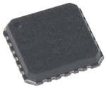
ICGOO电子元器件商城为您提供AD5700BCPZ-R5由Analog设计生产,在icgoo商城现货销售,并且可以通过原厂、代理商等渠道进行代购。 AD5700BCPZ-R5价格参考。AnalogAD5700BCPZ-R5封装/规格:接口 - 调制解调器 - IC 和模块, Modem HART 24-LFCSP-WQ (4x4)。您可以下载AD5700BCPZ-R5参考资料、Datasheet数据手册功能说明书,资料中有AD5700BCPZ-R5 详细功能的应用电路图电压和使用方法及教程。
AD5700BCPZ-R5是Analog Devices Inc.推出的一款低功耗、单片HART®(Highway Addressable Remote Transducer)调制解调器IC,主要应用于工业自动化和过程控制系统中。该器件专为支持HART通信协议而设计,广泛用于智能变送器、温度传感器、压力变送器、流量计和阀门定位器等现场仪表设备。

其典型应用场景包括在4-20mA模拟电流环路中叠加数字信号,实现双向通信,使控制系统能够在不中断模拟信号的前提下,读取设备状态、校准参数或诊断信息。AD5700BCPZ-R5集成高精度振荡器,无需外部晶振,减小了电路板空间和成本,特别适合对尺寸和功耗敏感的电池供电或回路供电设备。

该芯片工作温度范围宽(-40°C至+125°C),采用小型3mm × 3mm 16引脚LFCSP封装,具备良好的抗干扰能力和稳定性,适用于严苛的工业环境。凭借低功耗特性与高集成度,AD5700BCPZ-R5成为工业物联网(IIoT)和智能工厂中实现设备智能化、远程监控与预测性维护的理想选择。
| 参数 | 数值 |
| 产品目录 | 集成电路 (IC)半导体 |
| 描述 | IC INTERFACE MODEM接口 - 专用 HART Industrial Comm IC Low Pwr Modem |
| DevelopmentKit | DEMO-AD5700D2Z |
| 产品分类 | |
| 品牌 | Analog Devices Inc |
| 产品手册 | |
| 产品图片 |
|
| rohs | 符合RoHS无铅 / 符合限制有害物质指令(RoHS)规范要求 |
| 产品系列 | 接口 IC,接口 - 专用,Analog Devices AD5700BCPZ-R5- |
| 数据手册 | |
| 产品型号 | AD5700BCPZ-R5 |
| PCN组件/产地 | |
| 产品种类 | |
| 产品类型 | HART Modems |
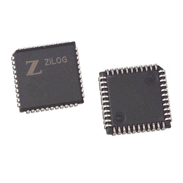
| 供应商器件封装 | 24-LFCSP-WQ(4x4) |
| 其它名称 | AD5700BCPZ-R5DKR |
| 包装 | Digi-Reel® |
| 商标 | Analog Devices |
| 安装类型 | 表面贴装 |
| 安装风格 | SMD/SMT |
| 封装 | Reel |
| 封装/外壳 | 24-WFQFN 裸露焊盘,CSP |
| 封装/箱体 | LFCSP-24 |
| 工作电源电压 | 2 V to 5.5 V |
| 工厂包装数量 | 500 |
| 数据格式 | HART |
| 最大工作温度 | + 125 C |
| 最小工作温度 | - 40 C |
| 标准包装 | 1 |
| 波特率 | - |
| 特色产品 | http://www.digikey.cn/product-highlights/cn/zh/analog-devices-ad5700-hart-modem/2801http://www.digikey.cn/product-highlights/zh/cn0267-field-instrument/50101 |
| 电压-电源 | 1.71 V ~ 5.5 V |
| 电源电压-最大 | 5.5 V |
| 电源电流 | 179 uA |
| 系列 | AD5700 |
| 视频文件 | http://www.digikey.cn/classic/video.aspx?PlayerID=1364138032001&width=640&height=505&videoID=2219598720001 |


- 商务部:美国ITC正式对集成电路等产品启动337调查
- 曝三星4nm工艺存在良率问题 高通将骁龙8 Gen1或转产台积电
- 太阳诱电将投资9.5亿元在常州建新厂生产MLCC 预计2023年完工
- 英特尔发布欧洲新工厂建设计划 深化IDM 2.0 战略
- 台积电先进制程称霸业界 有大客户加持明年业绩稳了
- 达到5530亿美元!SIA预计今年全球半导体销售额将创下新高
- 英特尔拟将自动驾驶子公司Mobileye上市 估值或超500亿美元
- 三星加码芯片和SET,合并消费电子和移动部门,撤换高东真等 CEO
- 三星电子宣布重大人事变动 还合并消费电子和移动部门
- 海关总署:前11个月进口集成电路产品价值2.52万亿元 增长14.8%


PDF Datasheet 数据手册内容提取
Low Power HART Modem Data Sheet AD5700/AD5700-1 FEATURES GENERAL DESCRIPTION HART-compliant fully integrated FSK modem The AD5700/AD5700-1 are single-chip solutions, designed 1200 Hz and 2200 Hz sinusoidal shift frequencies and specified to operate as a HART® FSK half-duplex modem, 115 µA maximum supply current in receive mode complying with the HART physical layer requirements. The Suitable for intrinsically safe applications AD5700/AD5700-1 integrate all of the necessary filtering, signal Integrated receive band-pass filter detection, modulating, demodulating and signal generation Minimal external components required functions, thus requiring few external components. The 0.5% Clocking optimized for various system configurations precision internal oscillator on the AD5700-1 greatly reduces Ultralow power crystal oscillator (60 µA maximum) the board space requirements, making it ideal for line-powered External CMOS clock source applications in both master and slave configurations. The maxi- Precision internal oscillator (AD5700-1only) mum supply current consumption is 115 µA, making the AD5700/ Buffered HART output—extra drive capability AD5700-1 an optimal choice for low power loop-powered applica- 8 kV HBM ESD rating tions. Transmit waveforms are phase continuous 1200 Hz and 1.71 V to 5.5 V power supply 2200 Hz sinusoids. The AD5700/AD5700-1 contain accurate 1.71 V to 5.5 V interface carrier detect circuitry and use a standard UART interface. −40°C to +125°C operation 4 mm × 4 mm LFCSP package Table 1. Related Products Part No. Description HART physical layer compliant UART interface AD5755-1 Quad-channel, 16-bit, serial input, 4 mA to 20 mA and voltage output DAC, dynamic power control, HART APPLICATIONS connectivity Field transmitters AD5421 16-bit, serial input, loop powered, 4 mA to 20 mA DAC AD5410/ Single-channel, 12-bit/16-bit, serial input, 4 mA to 20 mA HART multiplexers AD5420 current source DACs PLC and DCS analog I/O modules AD5412/ Single-channel, 12-bit/16-bit, serial input, current HART network connectivity AD5422 source and voltage output DACs FUNCTIONAL BLOCK DIAGRAM REG_CAP CLKOUT XTAL1 XTAL2 XTAL_EN VCC IOVCC OSC AD5700/AD5700-1 DUPLEX CD BUFFER FSK DAC HART_OUT C MODULATOR RXD OGI L OL ADC_IP TXD R ONT FSK ADC BFIALNTEDR-PAANSDS HART_IN RTS C DEMODULATOR BIASING CLK_CFG0 VOLTAGE REFERENCE CLK_CFG1 RESET DGND REF REF_EN AGND FILTER_SEL 10435-001 Figure 1. Rev. G Document Feedback Information furnished by Analog Devices is believed to be accurate and reliable. However, no responsibility is assumed by Analog Devices for its use, nor for any infringements of patents or other One Technology Way, P.O. Box 9106, Norwood, MA 02062-9106, U.S.A. rights of third parties that may result from its use. Specifications subject to change without notice. No license is granted by implication or otherwise under any patent or patent rights of Analog Devices. Tel: 781.329.4700 ©2012–2016 Analog Devices, Inc. All rights reserved. Trademarks and registered trademarks are the property of their respective owners. Technical Support www.analog.com
AD5700/AD5700-1 Data Sheet TABLE OF CONTENTS Features .....................................................................................1 FSK Modulator .................................................................... 13 Applications...............................................................................1 Connecting to HART_OUT ................................................ 14 General Description ..................................................................1 FSK Demodulator................................................................ 14 Functional Block Diagram.........................................................1 Connecting to HART_IN or ADC_IP ................................. 14 Revision History ........................................................................2 Clock Configuration ............................................................ 15 Specifications .............................................................................3 Supply Current Calculations................................................ 16 Timing Characteristics...........................................................5 Power-Down Mode ............................................................. 16 Absolute Maximum Ratings ......................................................6 Full Duplex Operation......................................................... 16 Thermal Resistance ................................................................6 Applications Information ........................................................ 17 ESD Caution ..........................................................................6 Supply Decoupling............................................................... 17 Pin Configuration and Function Descriptions...........................7 Transient Voltage Protection................................................ 17 Typical Performance Characteristics .........................................9 Typical Connection Diagrams ............................................. 18 Terminology ............................................................................12 Outline Dimensions ................................................................ 21 Theory of Operation................................................................13 Ordering Guide ................................................................... 21 REVISION HISTORY 12/2016—Rev. F to Rev. G 7/2012—Rev. A to Rev. B Changes to Figure 2 and Table 6 ................................................7 Removed V and IOV Current Consumption Text, Table 2.. 3 CC CC Added Internal Oscillator and External Clock Parameters 1/2014—Rev. E to Rev. F to Table 2 ................................................................................... 4 Changes to Figure 3 to Figure 7 .................................................9 Changes to t Description and Endnote 2, Table 3..................... 5 2 Changes to Example Section....................................................14 Changes to IOV Description, Table 6 ..................................... 7 CC Added Supply Current Calculations Section ........................... 16 10/2013—Rev. D to Rev. E Added Transient Voltage Protection Section, Figure 26, and Changes to t and t Descriptions, Table 3..................................5 Figure 27; Renumbered Sequentially ....................................... 17 7 8 Changed θ from 30°C/W to 56°C/W .......................................6 Changes to Typical Connection Diagrams Section.................. 18 JA Added Figure 13 and Figure 14................................................10 Changes to Figure 29. .............................................................. 19 Changes to External Crystal Section and Figure 25 .................15 Changes to Figure 30. .............................................................. 20 Updated Outline Dimensions.................................................. 21 5/2013—Rev. C to Rev. D 4/2012—Rev. 0 to Rev. A 2/2013—Rev. B to Rev. C Change to Transmit Impedance Parameter, RTS Low, Table 2 .. 4 Changed 2 V to 5.5 V Power Supply to 1.71 V to 5.5 V Power Changes to Figure 3, Figure 4, Figure 5, and Figure 7................ 9 Supply, Features Section ............................................................1 Changes to Figure 10 and Figure 11 ........................................ 10 Changes to Summary Statement, VCC Parameter, and Internal Changed AD5755 to AD5755-1 Throughout .......................... 17 Reference Voltage Parameter Test Conditions/Comments, Change to Figure 27 ................................................................ 18 Table 2 .......................................................................................3 Changed VCC = 2 V to 5.5 V to VCC = 1.71 V to 5.5 V in the 2/2012—Revision 0: Initial Version Summary Statement, Table 3 .....................................................5 Changes to Pin 18 Description and EPAD Mnemonic and Description, Table 6 ...................................................................7 Changes to Figure 9 and Figure 13 ..........................................10 Changes to Figure 28 ...............................................................18 Change to Figure 30.................................................................20 Rev. G | Page 2 of 24
Data Sheet AD5700/AD5700-1 SPECIFICATIONS V = 1.71 V to 5.5 V, IOV = 1.71 V to 5.5 V, AGND = DGND, CLKOUT disabled, HART_OUT with 5 nF load, internal and external CC CC receive filter, internal reference; all specifications are from −40°C to +125°C and relate to both A and B models, unless otherwise noted. Table 2. Parameter1 Min Typ Max Unit Test Conditions/Comments POWER REQUIREMENTS2 V 1.71 5.5 V CC IOV 1.71 5.5 V CC V and IOV Current Consumption CC CC Demodulator 86 115 µA B model, external clock, −40°C to +85°C 179 µA B model, external clock, −40°C to +125°C 69 97 µA B model, external clock, −40°C to +85°C, external reference 157 µA B model, external clock, −40°C to +125 °C, external reference 260 µA A model, external clock, −40°C to +125°C Modulator 124 140 µA B model, external clock, −40°C to +85°C 193 µA B model, external clock, −40°C to +125°C 73 96 µA B model, external clock, −40°C to +85°C, external reference 153 µA B model, external clock, −40°C to +125°C, external reference 270 µA A model, external clock, −40°C to +125°C Crystal Oscillator3 33 60 µA External crystal, 16 pF at XTAL1 and XTAL2 44 71 µA External crystal, 36 pF at XTAL1 and XTAL2 Internal Oscillator4 218 285 µA AD5700-1 only, external crystal not required Power-Down Mode RESET = REF_EN = DGND 16 35 µA Internal reference disabled, −40°C to +85°C 75 µA Internal reference disabled, −40°C to +125°C INTERNAL VOLTAGE REFERENCE Internal Reference Voltage 1.47 1.5 1.52 V REF_EN = IOVCC to enable use of internal reference; V = 1.71 V minimum CC Load Regulation 18 ppm/µA Tested with 50 µA load OPTIONAL EXTERNAL VOLTAGE REFERENCE External Reference Input Voltage 2.47 2.5 2.53 V REF_EN = DGND to enable use of external reference, V = 2.7 V minimum CC External Reference Input Current Demodulator 16 21 µA Current required by external reference in receive mode Modulator 28 33 µA Current required by external reference in transmit mode Internal Oscillator 5.5 7 µA Current required by external reference if using internal oscillator Power-Down 4.6 8.6 µA DIGITAL INPUTS V , Input High Voltage 0.7 × IOV V IH CC V , Input Low Voltage 0.3 × IOV V IL CC Input Current −0.1 +0.1 µA Input Capacitance5 5 pF Per pin Rev. G | Page 3 of 24
AD5700/AD5700-1 Data Sheet Parameter1 Min Typ Max Unit Test Conditions/Comments DIGITAL OUTPUTS V , Output High Voltage IOV − 0.5 V OH CC V , Output Low Voltage 0.4 V OL CD Assert6 85 100 110 mV p-p HART_IN INPUT5 Input Voltage Range 0 REF V External reference source 0 1.5 V Internal reference enabled HART_OUT OUTPUT Output Voltage 459 493 505 mV p-p AC-coupled (2.2 µF), measured at HART_OUT pin with 160 Ω load (worst-case load), see Figure 17 and Figure 18 for HART_OUT voltage vs. load Mark Frequency7 1200 Hz Internal oscillator Space Frequency7 2200 Hz Internal oscillator Frequency Error −0.5 +0.5 % Internal oscillator, −40°C to +85°C −1 +1 % Internal oscillator, −40°C to +125°C Phase Continuity Error5 0 Degrees Maximum Load Current5 160 Ω Worst-case load is 160 Ω, ac-coupled with 2.2 µF, see Figure 21 for recommended configuration if driving a resistive load Transmit Impedance 7 Ω RTS low, at the HART_OUT pin 70 kΩ RTS high, at the HART_OUT pin INTERNAL OSCILLATOR Frequency 1.2226 1.2288 1.2349 MHz −40°C to +85°C 1.2165 1.2288 1.2411 MHz −40°C to +125°C EXTERNAL CLOCK External Clock Source Frequency 3.6496 3.6864 3.7232 MHz 1 Temperature range: −40°C to +125°C; typical at 25°C. 2 Current consumption specifications are based on mean current values. 3 The demodulator and modulator currents are specified using an external clock. If using an external crystal oscillator, the crystal oscillator current specification must be added to the corresponding VCC and IOVCC demodulator/modulator current specification to obtain the total supply current required in this mode. 4 The demodulator and modulator currents are specified using an external clock. If using the internal oscillator, the internal oscillator current specification must be added to the corresponding VCC and IOVCC demodulator/modulator current specification to obtain the total supply current required in this mode. 5 Guaranteed by design and characterization, but not production tested. 6 Specification set assuming a sinusoidal input signal containing preamble characters at the input and an ideal external filter (see Figure 23). 7 If the internal oscillator is not used, frequency accuracy is dependent on the accuracy of the crystal or clock source used. Rev. G | Page 4 of 24
Data Sheet AD5700/AD5700-1 TIMING CHARACTERISTICS V = 1.71 V to 5.5 V, IOV = 1.71 V to 5.5 V, T to T , unless otherwise noted. CC CC MIN MAX Table 3. Parameter1 Limit at T , T Unit Description MIN MAX t1 1 Bit time2 max Carrier start time. Time from RTS falling edge to carrier reaching its first peak. See Figure 3. t2 1 Bit time2 max Carrier stop time. Time from RTS rising edge to carrier amplitude dropping below the minimum receive amplitude. t3 1 Bit time2 max Carrier decay time. Time from RTS rising edge to carrier amplitude dropping to ac zero. See Figure 4. t 6 Bit times2 max Carrier detect on. Time from carrier on to CD rising edge. See Figure 5. 4 t 6 Bit times2 max Carrier detect off. Time from carrier off to CD falling edge. See Figure 6. 5 t 10 Bit times2 max Carrier detect on when switching from transmit mode to receive mode in the 6 presence of a constant valid carrier. Time from RTS rising edge to CD rising edge. See Figure 7. t 2.1 ms typ Crystal oscillator power-up time. On application of a valid power supply voltage at 7 VCC or on enabling of the oscillator via the XTAL_EN pin. Crystal load capacitors = 16 pF. t 6 ms typ Crystal oscillator power-up time. Crystal load capacitors = 36 pF. 8 t 25 µs typ Internal oscillator power-up time. On application of a valid power supply voltage 9 at V or on enabling of the oscillator via the CLK_CFG0 and CLK_CFG1 pins. CC t 10 ms typ Reference power-up time. 10 t 30 µs typ Transition time from power-down mode to normal operating mode (external 11 clock source, external reference). 1 Specifications apply to AD5700/AD5700-1 configured with internal or external receive filter. 2 Bit time is the length of time to transfer one bit of data (1 bit time = 1/1200 Hz = 833.333 µs). Rev. G | Page 5 of 24
AD5700/AD5700-1 Data Sheet ABSOLUTE MAXIMUM RATINGS T = 25°C, unless otherwise noted. A Stresses at or above those listed under Absolute Maximum Transient currents of up to 100 mA do not cause SCR latch-up. Ratings may cause permanent damage to the product. This is a stress rating only; functional operation of the product at these Table 4. or any other conditions above those indicated in the operational Parameter Rating section of this specification is not implied. Operation beyond V to GND −0.3 V to +7 V CC the maximum operating conditions for extended periods may IOV to GND −0.3 V to +7 V CC affect product reliability. Digital Inputs to DGND −0.3 V to IOVCC + 0.3 V or +7 V (whichever is less) THERMAL RESISTANCE Digital Output to DGND −0.3 V to IOVCC + 0.3 V or θ is specified for the worst-case conditions, that is, a device +7 V (whichever is less) JA soldered in a circuit board for surface-mount packages. HART_OUT to AGND −0.3 V to +2.5 V HART_IN to AGND −0.3 V to VCC + 0.3 V or Table 5. Thermal Resistance +7 V (whichever is less) Package Type θ 1 θ Unit JA JC ADC_IP −0.3 V to VCC + 0.3 V or 24-Lead LFCSP 56 3 °C/W +7 V (whichever is less) AGND to DGND −0.3 V to +0.3 V 1 Thermal impedance simulated values are based on JEDEC 2S2P thermal test Operating Temperature Range (T) board with thermal vias. See JEDEC JESD51. A Industrial −40°C to +125°C ESD CAUTION Storage Temperature Range −65°C to +150°C Junction Temperature (T ) 150°C JMAX Power Dissipation (T – T)/θ JMAX A JA Lead Temperature, JEDEC industry standard Soldering J-STD-020 ESD Human Body Model 8 kV (ANSI/ESDA/JEDEC JS-001- 2010) Field Induced Charge Model 1.5 kV (JEDEC JESD22_C101E) Machine Model 400 V (ANSI/ESD S5.2-2009) Rev. G | Page 6 of 24
Data Sheet AD5700/AD5700-1 PIN CONFIGURATION AND FUNCTION DESCRIPTIONS L E S _RETLIF NE_FER DNGD 1LATX 2LATX DNGA 42 32 22 12 02 91 XTAL_EN1 18VCC CLKOUT2 17ADC_IP AD5700/ CLK_CFG03 AD5700-1 16HART_IN CLK_CFG14 TOP VIEW 15REF (Not to Scale) RESET5 14HART_OUT CD6 13REG_CAP 7 8 9 01 11 21 D S X D C D XT TR ELPU XR VOIC NGD D NOTES 1. THE EXPOSEDPADDLE MUST BE CONNECTED TOAGND OR DGND, OR,ALTERNATIVELY, IT CAN BE LEFT ELECTRICALLY UNCONNECTED. IT IS RCTHEOECNRONMMEACMLTE EPNDEDRTEOFDO ATR HCMAOATPN TPCHEEER. PPALDADNLEE F BOER T EHNEHRAMNACLELDY 10435-002 Figure 2. Pin Configuration Table 6. Pin Function Descriptions Pin No. Mnemonic Description 1 XTAL_EN Crystal Oscillator Circuit Enable. A low state enables the crystal oscillator circuit, and an external crystal is required. A high state disables the crystal oscillator circuit, and an external clock source or the internal oscillator (AD5700-1only) provides the clock source. This pin is used in conjunction with the CLK_CFG0 and CLK_CFG1 pins in configuring the required clock generation scheme. 2 CLKOUT Clock Output. If using the crystal oscillator or the internal RC oscillator, a clock output can be configured at the CLKOUT pin. Enabling the clock output consumes extra current to drive the load on this pin. See the CLKOUT section for more details. 3 CLK_CFG0 Clock Configuration Control. See Table 7. 4 CLK_CFG1 Clock Configuration Control. See Table 7. 5 RESET Active Low Digital Input. Holding RESET low places the AD5700/AD5700-1 in power-down mode. A high state on RESET returns the AD5700/AD5700-1 to their power-on state. If not using this pin, tie this pin to IOV . CC 6 CD Carrier Detect—Digital Output. A high on CD indicates a valid carrier is detected. 7 TXD Transmit Data—Digital Input. Data input to the modulator. 8 RTS Request to Send—Digital Input. A high state enables the demodulator and disables the modulator. A low state enables the modulator and disables the demodulator. 9 DUPLEX A high state on this pin enables full duplex operation. See the Theory of Operation section. A low state disables this feature. 10 RXD Receive Data—UART Interface Digital Data Output. Data output from the demodulator is accessed on this pin. 11 IOV Digital Interface Supply. Digital threshold levels are referenced to the voltage applied to this pin. The applied CC voltage can be in the range of 1.71 V to 5.5 V. IOV should be decoupled to ground with low ESR 10 μF and CC 0.1 μF capacitors (see the Supply Decoupling section). 12 DGND Digital Circuitry Ground Reference Connection. For typical operation, it is recommended to connect this pin to AGND. 13 REG_CAP Capacitor Connection for Internal Voltage Regulator. Connect a 1 μF capacitor from this pin to ground. Connect REG_CAP to V when V ≤ 1.98 V. CC CC 14 HART_OUT HART FSK Signal Output. See the FSK Modulator section and Figure 30 for typical connections. 15 REF Internal Reference Voltage Output, or External 2.5 V Reference Voltage Input. Connect a 1 μF capacitor from this pin to ground. When supplying an external reference, the VCC supply requires a minimum voltage of 2.7 V. 16 HART_IN HART FSK Signal. When using the internal filter, couple the HART input signal into this pin using a 2.2 nF series capacitor. If using an external band-pass filter as shown in Figure 23, do not connect to this pin. 17 ADC_IP If using the internal band-pass filter, connect 680 pF to this pin. Alternatively, this pin allows direct connection to the ADC input, in which case an external band-pass filter network must be used, as shown in Figure 23. Rev. G | Page 7 of 24
AD5700/AD5700-1 Data Sheet Pin No. Mnemonic Description 18 VCC Power Supply Input. 1.71 V to 5.5 V can be applied to this pin. VCC should be decoupled to ground with low ESR 10 µF and 0.1 µF capacitors (see the Supply Decoupling section). 19 AGND Analog Circuitry Ground Reference Connection. 20 XTAL2 Connection for External 3.6864 MHz Crystal. Do not connect to this pin if using the internal RC oscillator (AD5700-1 only) or an external clock source. 21 XTAL1 Connection for External 3.6864 MHz Crystal or External Clock Source Input. Tie this pin to ground if using the internal RC oscillator (AD5700-1 only). 22 DGND Digital Circuitry Ground Reference Connection. For typical operation, it is recommended to connect this pin to AGND. 23 REF_EN Reference Enable. A high state enables the internal 1.5 V reference and buffer. A low state disables the internal reference and input buffer, and a buffered external 2.5 V reference source must be applied at REF. If REF_EN is tied low, V must be greater than 2.7 V. CC 24 FILTER_SEL Band-Pass Filter Select. A high state enables the internal filter and the HART signal should be applied to the HART_IN pin. A low state disables the internal filter and an external band-pass filter must then be connected at the ADC_IP input pin. In this case, the HART signal should be applied to the ADC_IP pin. EPAD EPAD The exposed paddle must be connected to AGND or DGND, or, alternatively, it can be left electrically unconnected. It is recommended that the paddle be thermally connected to a copper plane for enhanced thermal performance. Rev. G | Page 8 of 24
Data Sheet AD5700/AD5700-1 TYPICAL PERFORMANCE CHARACTERISTICS 1.4 1.4 TA = 25°C; VCC = IOVCC = 3.3V; INT VREF TA = 25°C; VCC = IOVCC = 3.3V; INT VREF 1.2 RTS AND TXD DC LEVELS HAVE BEEN ADJUSTED FOR 1.2 CDAND RXD DC LEVELS HAVE BEENADJUSTED FOR CLARITY. IN REALITY, BOTH OF THESE SIGNALS RANGE CLARITY. IN REALITY, BOTH OF THESE SIGNALS RANGE FROM 0V TO 3.3V. FROM 0VTO 3.3V. 1.0 1.0 RTS CD t5 UT (V) 00..86 t1 NAL (V) 00..86 RT_O 0.4 TXD T SIG 0.4 RXD A R H A 0.2 H 0.2 HART SIGNAL 0 0 HART_OUT –0.2 –0.2 –0.–40.3 0 0.3 0.6 TIM0E. 9(ms) 1.2 1.5 1.8 2.110435-003 –0.4–5 –4 –3 TIME– 2(ms) –1 0 1 10435-006 Figure 3. Carrier Start Time Figure 6. Carrier Detect Off Timing 1.4 1.50 TA = 25°C; VCC = IOVCC = 3.3V; INT VREF TA = 25°C; VCC = IOVCC = 3.3V; INT VREF 1.2 RCTLSA RAINTYD. TINX DR EDACL LITEYV,E BLOST HHA OVEF TBHEEESNE A SDIJGUNSATLESD R FAONRGE 1.25 RCTLSA RAINTYD. CIND RDECA LLEITVYE,L BSO HTAHV OEF B TEHEENS AED SJIUGSNTAELDS FROARNGE FROM 0V TO 3.3V. 1.00 FROM 0V TO 3.3V. 1.0 RTS t6 0.8 RTS t2 0.75 UT (V) 0.6 TXD t3 UT (V) 0.50 CD HART SIGNAL HAS ALSO _O _O 0.25 BEEN OFFSET BY –0.6V. RT 0.4 RT A HART_OUT A 0 H H 0.2 HART_OUT –0.25 0 –0.50 –0.2 –0.75 HART SIGNAL –0.–42.0 –1.5 –1.0 TIM–E0 .(5ms) 0 0.5 1.010435-004 –1.00–10 –7.5 –5.0TIME (ms–)2.5 0 2.510435-007 Figure 4. Carrier Stop/Decay Time Figure 7. Carrier Detect on When Switching from Transmit Mode to Receive Mode in the Presence of a Constant Valid Carrier 1.4 100 TA = 25°C; VCC = IOVCC = 3.3V; INT VREF TA = 25°C 1.2 CD AND RXD DC LEVELS HAVE BEEN ADJUSTED FOR 90 VCC = IOVCC = 2.7V TO 5.5V 1.0 CFRLAORMI T0YV. TINO R3E.3AVL.ITY, BOTH OF THESE SIGNALS RANGE 80 DEV 1 EXT REF MOD ICCAND IOICC CD t4 A) 70 L (V) 0.8 NT (µ 60 DEMOD ICC AND IOICC NA 0.6 RE HART SIG 00..42 RXD UPPLY CUR 543000 MOD IREF S 0 HART SIGNAL 20 DEMOD IREF –0.2 10 –0.–40.5 0 0.5 TIM1E. 0(ms) 1.5 2.0 2.510435-005 02.0 2.5 3.0 3.V5CC = I4O.0VCC (V4).5 5.0 5.5 6.010435-008 Figure 5. Carrier Detect On Timing Figure 8. Supply Currents vs. Supply Voltage—External Reference Rev. G | Page 9 of 24
AD5700/AD5700-1 Data Sheet 200 0 180 DTVACE CV= =12 5IIO°NCVTC RCE =F 1.71V TO 5.5V –2 VTAC C= =2 5IO°CVCC = 3.3V REG_CAP IS CONNECTED INT VREF 160 TO VCC FOR SUPPLIES OF ≤ 2.0V –4 140 –6 A) (µCC120 MOD ICCAND IOICC B) –8 ND IOI 100 AIN (d–10 A 80 G–12 I CC 60 DEMOD ICC AND IOICC –14 EXTERNAL FILTER INTERNAL FILTER 40 –16 20 –18 01.0 1.5 2.0 2.5 V3C.0C = I3O.5VCC 4(V.0) 4.5 5.0 5.5 6.010435-026 –20100 FRE1QkUENCY (Hz) 10k 10435-011 Figure 9. Supply Currents vs. Supply Voltage—Internal Reference Figure 12. Input Filter Frequency Response 700 2.5 TA = 25°C; VCC = IOVCC = 3.3V; INT VREF TA = 25°C CLK CONFIG = XTAL OSCILLATOR VCC = IOVCC = 2V 600 IOICC = 41µA 2.0 500 CURRENT (µA)CC430000 TTXXDD == 10 CD VOLTAGE (V) 11..05 I200 2.2µF HART_OUT 0.5 100 22nF RLOAD 00 200 RLO4A0D0 (Ω) WIT6H00 22nF TO80 G0ND 1000 120010435-009 00 0.2 0.4 0.6 CD0 .C8URR1.E0NT (1m.2A) 1.4 1.6 1.8 2.0 10435-032 Figure 10. Current in Tx Mode vs. Resistive Load Figure 13. Carrier Detect—Voltage vs. Current, 2 V 250 3.5 TA = 25°C; VCC = IOVCC = 3.3V; INT VREF TA = 25°C 225 CLK CONFIG = XTAL OSCILLATOR VCC = IOVCC = 3.3V CAPACITIVE LOAD ONLY 3.0 200 IOICC = 41µA 175 2.5 CURRENT (µA)CC111520050 CD VOLTAGE (V) 12..50 I 75 1.0 TXD = 1 50 TXD = 0 0.5 25 0 0 0 10 20 CLOA3D0 (nF) 40 50 6010435-010 0 1 2 CD C3URRENT4 (mA) 5 6 7 10435-033 Figure 11. Current in Tx Mode vs. Capacitive Load Figure 14. Carrier Detect—Voltage vs. Current, 3.3 V Rev. G | Page 10 of 24
Data Sheet AD5700/AD5700-1 1.5012 500 TA = 25°C TA = 25°C 1.5010 VCC = IOVCC = 1.71VTO 5.5V VCC = IOVCC = 3.3V 495 INT VREF 1.5008 490 NAL (V)11..55000064 mV p-p) 485 INTEREF1.5002 RT_OUT ( 480 12220000HHzz VR1.5000 HA 475 2.2µF 1.4998 HART_OUT 470 22nF RLOAD 1.4996 1.49941.0 1.5 2.0 2.5 3.0 VC3C. 5(V) 4.0 4.5 5.0 5.5 6.0 10435-012 4650 200 RLO4A0D0 (Ω) || W6IT0H0 22nF T8O0 0GND 1000 120010435-014 Figure 15. Reference Voltage vs. VCC Figure 17. HART_OUT Voltage vs. RLOAD 1.5006 505 1.5004 VTECCM P= EIORVACTCU R= E2 .=7 V–40°CTO +125°C 504 VTAC C= =2 5IO°CVCC = 3.3V INT VREF 503 CAPACITIVE LOAD ONLY 1.5002 NAL (V)1.5000 mV p-p)550012 NTER1.4998 OUT (500 IEF1.4996 RT_499 1200Hz VR HA498 2200Hz 1.4994 497 1.4992 496 1.4990–40 –20 0 2T0EMPE4R0ATURE60 (°C) 80 100 120 10435-013 4950 10 20 CLOA3D0 (nF) 40 50 6010435-015 Figure 16. Reference Voltage vs. Temperature Figure 18. HART_OUT Voltage vs. CLOAD Rev. G | Page 11 of 24
AD5700/AD5700-1 Data Sheet TERMINOLOGY HART_OUT Output Voltage V and IOV Current Consumption CC CC This is the peak-to-peak HART_OUT output voltage. The This specification gives a summation of the current consump- specification in Table 2 was set using a worst-case load of 160 Ω, tion of both the V and the IOV supplies. Figure 11 shows CC CC ac-coupled with a 2.2 µF capacitor. Figure 17 and Figure 18 show separate measurements for V and IOV currents vs. varying CC CC HART_OUT output voltages for both resistive and purely capacitive loads, in transmit mode. capacitive loads. Load Regulation Mark/Space Frequency Load regulation is the change in reference output voltage due to A 1.2 kHz signal represents a digital 1, or mark, whereas a a specified change in load current. It is expressed in ppm/µA. 2.2 kHz signal represents a 0, or space. CD Assert Phase Continuity Error The minimum value at which the carrier detect signal asserts is The DDS engine in this design inherently generates continuous 85 mV p-p and the maximum value it asserts at is 110 mV p-p. CD phase signals, thus avoiding any output discontinuity when is already high (asserted) for HART input signals greater than switching between frequencies. This attribute is desirable for 110 mV p-p. This specification was set assuming a sinusoidal signals that are to be transmitted over a band limited channel, input signal containing preamble characters at the input and an because discontinuities in a signal introduce wideband fre- ideal external filter (see Figure 23). quency components. As the name suggests, for a signal to be continuous, the phase continuity error must be 0o. Rev. G | Page 12 of 24
Data Sheet AD5700/AD5700-1 THEORY OF OPERATION FSK MODULATOR Highway Addressable Remote Transducer (HART) Communica- tion is the global standard for sending and receiving digital The modulator converts a bit stream of UART-encoded HART information across analog wires between smart field devices data at the TXD input to a sequence of 1200 Hz and 2200 Hz and control systems. This is a digital two-way communication tones (see Figure 19). This sinusoidal signal is internally buff- system, in which a 1 mA p-p frequency shift keyed (FSK) signal ered and output on the HART_OUT pin. The modulator is is modulated on top of a 4 mA to 20 mA analog current signal. enabled by bringing the RTS signal low. The AD5700/AD5700-1 are designed and specified to operate as a single-chip, low power, HART FSK half-duplex modem, complying with the HART physical layer requirements "1" = MARK "0" = SPACE 1.2kHz 2.2kHz (Revision 8.1). A single-chip solution, the AD5700/AD5700-1 not only inte- grate the modulation and demodulation functions, but also contain an internal reference, an integrated receive band-pass START filter (which has the flexibility of being bypassed if required), TXD and an internally buffered HART output, giving a high output STOP drive capability and removing the need for external buffering. The AD5700-1 option also contains a precision internal RC oscillator. The block diagram in Figure 1 shows a graphical HART_OUT illustration of how these circuit blocks are connected together. As a result of such extensive integration options, minimal 8-BIT DATA +PARITY 10435-016 external components are required. The AD5700/AD5700-1 Figure 19. AD5700/AD5700-1 Modulator Waveform are suitable for use in both HART field instrument and master configurations. The modulator block contains a DDS engine that produces a 1.2 kHz or 2.2 kHz sine wave in digital form and then performs The AD5700/AD5700-1 either transmit or receive 1.2 kHz and a digital-to-analog conversion. This DDS engine inherently 2.2 kHz carrier signals. A 1.2 kHz signal represents a digital 1, generates continuous phase signals, thus avoiding any output or mark, whereas a 2.2 kHz signal represents a 0, or space. discontinuity when switching between frequencies. For more There are three main clocking configurations supported by information on DDS fundamentals, see MT-085, Fundamentals these parts, two of which are available on the AD5700 option, of Direct Digital Synthesizers (DDS). Figure 20 demonstrates a whereas all three are available on the AD5700-1 device: simple implementation of this FSK encoding. • External crystal 1 • CMOS clock input DATA 0 • Internal RC oscillator (AD5700-1 only) The device is controlled via a standard UART interface. The 1.2kHz relevant signals are RTS, CD, TXD, and RXD (see Table 6 for WORD MUX DDS DAC FSK more detail on individual pin descriptions). 2.2kHz WORD CLOCK 10435-017 Figure 20. DDS-Based FSK Encoder Rev. G | Page 13 of 24
AD5700/AD5700-1 Data Sheet CONNECTING TO HART_OUT FSK DEMODULATOR The HART_OUT pin is dc biased to 0.75 V and should be capacitively coupled to the load. The current consumption HART_IN specifications in Table 2 are based on driving a 5 nF load. If the application requires a larger load value, more current is 8-BIT DATA +PARITY required. This value can be calculated from the following RXD formuIla: =I +I START STOP 10435-019 TOTAL AD5700 LOADRMS Figure 22. AD5700/AD5700-1 Demodulator Waveform 500mV (Preamble Message 0xFF) I = (1) LOADRMS 1 2 When RTS is logic high, the modulator is disabled and the 4 2× 2π×f×C +RLOAD2 demodulator is enabled, that is, the AD5700/AD5700-1 are in LOAD receive mode. A high on CD indicates a valid carrier is detected. where: The demodulator accepts an FSK signal at the HART_IN pin I is the current drawn by the AD5700/AD5700-1 in and restores the original modulated signal at the UART AD5700 transmit mode as per specifications (see Table 2). Note that the interface digital data output pin, RXD. The combination of the specifications in Table 2 assume a 5 nF C . ADC, digital filtering and digital demodulation results in a LOAD f is the output frequency (1.2 kHz or 2.2 kHz). highly accurate output on the RXD pin. The HART bit stream C is the capacitive load to ground on HART_OUT. follows a standard UART frame with a start bit, 8-bit data, one LOAD R is the resistive load on the loop. parity, and a stop bit (see Figure 22). LOAD CONNECTING TO HART_IN OR ADC_IP When driving a purely capacitive load, the load should be in the range of 5 nF to 52 nF. See Figure 11 for a typical plot of supply The AD5700/AD5700-1 have two filter configuration options: current vs. capacitive load. an external filter (HART signal is applied to ACP_IP) and an Example internal filter (HART signal is applied to HART_IN). Assume use of an internal reference, and C = 52 nF. The external filter configuration is shown in Figure 23. In this LOAD case, the HART signal is applied to the ADC_IP pin through an I + IOI = 140 µA maximum (from Table 2 CC CC external filter circuit. In safety critical applications, the AD5700/ specification) AD5700-1 must be isolated from the high voltage of the loop Note that this is incorporating a 5 nF load. supply. The recommended external band-pass filter includes a Therefore, to calculate the load current required to drive the 150 kΩ resistor, which limits current to a sufficiently low level extra 47 nF, use Equation 1. to adhere to intrinsic safety requirements. In this case, the input has higher transient voltage protection and should, therefore, Substituting f = 1200 Hz, C = 47 nF, and R = 0 Ω into LOAD LOAD not require additional protection circuitry, even in the most the formula results in I of 31.3 µA. LOAD demanding of industrial environments. Assuming the use of a If using the crystal oscillator, this adds 60 µA maximum (see 1% accurate resistor and 10% accurate capacitor components, Table 2 for conditions). the calculated variation in CD trip voltage levels vs. the ideal is Thus, the total worst-case current in this example is: ±3.5 mV. 140 µA + 31.3 µA + 60 µA = 231.3 µA HART_OUT If driving a load with a resistive element, it is recommended to AD5700/ HART place a 22 nF capacitor to ground at the HART_OUT pin. The AD5700-1 REF NETWORK load should be coupled with a 2.2 µF series capacitor. For low 1µF 1.2MΩ 150kΩ ADC_IP impedance devices, the R range is typically 230 Ω to 600 Ω. LOAD 2.2µF 1.2MΩ 300pF 150pF 10435-020 HART_OUT Figure 23. AD5700/AD5700-1 with External Filter on ADC_IP 22nF RLOAD 10435-018 Figure 21. AD5700/AD5700-1 with Resistive Load at HART_OUT Rev. G | Page 14 of 24
Data Sheet AD5700/AD5700-1 The internal filter configuration is shown in Figure 24. This CMOS Clock Input option is beneficial where cost or board space is a large concern A CMOS clock input can also be used to generate a clock for the because it removes the need for multiple external components. AD5700/AD5700-1. To use this mode, connect an external This configuration achieves an 8 kV ESD HBM rating but clock source to the XTAL 1 pin, and leave XTAL2 open circuit requires extra external protection circuitry for EMC and surge (see Figure 26). protection purposes if used in harsh industrial environments. HART_OUT HART AD5700/ 2.2nF NETWORK HART_IN 1 2 AD5700-1 L L A A 680pF T T Figure 24. AD5700/AADD5C7_0I0P-1 Using Internal Filter on HART_10435-021IN AD57X00/AD5X700-1 10435-027 CLOCK CONFIGURATION Figure 26. CMOS Clock Connection The AD5700/AD5700-1 support numerous clocking configura- Internal Oscillator (AD5700-1 only) tions to allow the optimal trade-off between cost and power: Consuming typically 218 µA, the low power, internal, 0.5 % • External crystal precision RC oscillator, available only on theAD5700-1, has an • CMOS clock input oscillation frequency of 1.2288 MHz. To use this mode, tie the • Internal RC oscillator (AD5700-1 only) XTAL1 pin to ground and leave the XTAL2 pin open circuit (see Figure 27). The CLK_CFG0, CLK_CFG1, and XTAL_EN pins configure the clock generation as shown in Table 7. The AD5700/AD5700-1 can also provide a clock output at CLKOUT (for more details, see the CLKOUT section). L1 L2 A A T T External Crystal X X AD5700-1 LT4hQe t-yTp) iicsa sl hcoownnne icnti oFnig fuorre a 2n5 e.x Tteor nenals curryes mtali n(AimBuLmS-3 c.6u8rr6e4nMt HZ- 10435-028 consumption and to minimize stray capacitances, connections Figure 27. Internal Oscillator Connection between the crystal, capacitors, and ground should be made as CLKOUT close to the AD5700/AD5700-1 as possible. Consult individual The AD5700/AD5700-1 can provide a clock output at CLKOUT crystal vendors for recommended load information and crystal (see Table 7). performance specifications. ABLS-3-6864MHZ-L4Q-T • If using the crystal oscillator, this clock output can be 36pF 36pF configured as a 3.6864 MHz, 1.8432 MHz, or 1.2288 MHz buffer clock. • If using a CMOS clock, no clock output can be configured 1 2 at the CLKOUT pin. L L TA TA • If using the internal RC oscillator, this clock output is only X X available as a 1.2288 MHz buffer clock. AD5700/AD5700-1 10435-022 tThheer eafmorpel,i tthued ec loofc tkh oe uctlpouckt coaunt pbuet idne tpheen rdasn ogne othf e1 .I7O1V VC Cp l-epv teol; Figure 25. Crystal Oscillator Connection 5.5 V p-p. Enabling the clock output of the AD5700/AD5700-1 The ABLS-3.6864MHZ-L4Q-T crystal oscillator data sheet increases the current consumption of the device. This increase recommended two 36 pF capacitors. Because the crystal current is due to the current required to drive any load at the CLKOUT consumption is dominated by the load capacitance, in an effort pin, which should not be more than 30 pF. to reduce the crystal current consumption, two 16 pF capacitors This capacitance should be minimized to reduce current were used on the XTAL1 and XTAL2 pins. The AD5700/AD5700-1 consumption and provide the clock with the cleanest edges. still functioned as expected, even with the resulting reduction in The additional current drawn from the IOV supply can be CC frequency performance from the crystal due to the smaller calculated using the following equation: capacitance values. Crystals are available that support 16 pF I = C × V × f capacitors. It is recommended to consult the relevant crystal manufacturers for this information. Rev. G | Page 15 of 24
AD5700/AD5700-1 Data Sheet Table 7. Clock Configuration Options XTAL_EN CLK_CFG1 CLK_CFG0 CLKOUT Description 1 0 0 No output 3.6864 MHz CMOS clock connected at XTAL1 pin 1 0 1 No output 1.2288 MHz CMOS clock connected at XTAL1 pin 1 1 0 No output Internal oscillator enabled (AD5700-1 only) 1 1 1 1.2288 MHz output Internal oscillator enabled, CLKOUT enabled (AD5700-1only) 0 0 0 No output Crystal oscillator enabled 0 0 1 3.6864 MHz output Crystal oscillator enabled, CLKOUT enabled 0 1 0 1.8432 MHz output Crystal oscillator enabled, CLKOUT enabled 0 1 1 1.2288 MHz output Crystal oscillator enabled, CLKOUT enabled SUPPLY CURRENT CALCULATIONS POWER-DOWN MODE The V and IOV current consumption specifications shown The AD5700/AD5700-1 can be placed into power-down mode CC CC in Table 2 are derived using the internal reference and an by holding the RESET pin low. If using the internal reference, it external clock source. This specification is given for a is recommended to tie the REF_EN pin to the RESET pin so maximum temperature of 85oC (115 µA receive current and that it is also powered down. If the reference is not powered 140 µA transmit current) and an extended maximum down while RESET is low, the output voltage on the REF pin is temperature of 125oC (179 µA receive current and 193 µA approximately 1.7 V until RESET is brought high again. transmit current). Alternatively, if the external reference is In this mode, the receive, transmit, and oscillator circuits are all preferred, (assuming a maximum temperature of 85oC), the switched off, and the device consumes a typical current of 16 µA. receive and transmit supply current values become 118 µA and 129 µA respectively, including the current required by the FULL DUPLEX OPERATION external reference. A similar calculation can be done for the Full duplex operation means that the modulator and demodula- 125oC maximum temperature case. tor of the AD5700/AD5700-1 are enabled at the same time. This If the crystal oscillator or internal oscillator is used, VCC and is a powerful feature, enabling a self-test procedure of not only IOVCC current consumption figures return to the 115 µA receive the HART device but also the complete signal path between the current and 140 µA transmit current. However, the resultant HART device and the host controller. This provides verification current consumption from the crystal oscillator or internal that the local communications loop is functional. This increased oscillator must now be accounted for, 60 µA maximum addi- level of system diagnostics is useful in production self-test and tional current for the crystal oscillator, or 285 µA maximum is advantageous in improving the application’s safety integrity additional current for the internal oscillator option. This gives level (SIL) rating. The full duplex mode of operation is enabled by a maximum current consumption of 175 µA in receive mode connecting the DUPLEX pin to logic high. and 200 µA in transmit mode, when using the internal reference and the crystal oscillator. Utilizing the internal reference and the internal oscillator (AD5700-1 only) results in a total maximum current consumption of 400 µA for receive current and 425 µA for transmit current. Rev. G | Page 16 of 24
Data Sheet AD5700/AD5700-1 APPLICATIONS INFORMATION SUPPLY DECOUPLING shows an example of a HART-enabled current input module that contains transient voltage protection circuitry, which is It is recommended to decouple the V and IOV supplies with CC CC very important in harsh industrial control environments. 10 μF in parallel with 0.1 μF capacitors to ground. For many The module is powered from a 24 V field supply, and the 250 Ω applications, 1 μF in parallel with 0.1 μF ceramic capacitors to load is within the low impedance module itself. This configuration ground should be sufficient. The REG_CAP voltage of 1.8 V is is in contrast to Figure 29, which demonstrates a secondary HART used to supply the AD5700/AD5700-1 internal circuitry and is device, in which the load is outside of the module. For transient derived from the V supply using a high efficiency clocking CC voltage protection, a 10 V unidirectional (for protection against LDO. Decouple this REG_CAP supply with a 1 μF ceramic positive high voltage transients) transient voltage suppressor (TVS) capacitor to ground. It is also required to decouple the REF pin is placed at the connection point of the current input module. with a 1 μF ceramic capacitor to ground. Place decoupling The TVS component that is used in a given application circuit capacitors as close to the relevant pins as possible. must have power ratings that are appropriate to the individual For loop-powered applications, it is recommended to connect a system. When choosing the TVS, low leakage current is also an resistance in series with the V supply to minimize the effect of CC important specification for maintaining the accuracy of the analog any noise, which may, depending on the system configuration, be current input. In the event of a transient spike, the 22 Ω series introduced onto the loop as a result of current draw variations resistor acts as a current limiting resistor for the FSK output pin. from the AD5700/AD5700-1. For typical applications, 470 Ω of The FSK input pin is inherently protected by the 150 kΩ resistor, resistance has proven most effective. However, depending on the which forms part of the recommended external filter circuitry application conditions, alternative values may also be acceptable at the FSK input. The voltage divider, made up of both a 75 kΩ (see R1 in Figure 31). resistor and a 22 kΩ resistor, is used to maintain a 0.75 V dc bias TRANSIENT VOLTAGE PROTECTION at the field side of the FSK output switch. Many industrial control applications have requirements for HART-enabled current input and output modules. Figure 28 3.3V 3.3V 2.2µF 75kΩ VCC HART_OUT TXD 22Ω 1400V0W 6.8nF 22kΩ 10nF AD5700/ RXD AD5700-1 RTS REF CD 1.2MΩ 1µF ENT VLO24OVP 115500kpΩF 300pF 1.2MΩ ADC_IAPGND CONMTICRROOLL-ER DM FIELTRU S N I 20kΩ ADC 250Ω 10µF 10435-031 Figure 28. Current Input Module, HART Circuit 3.3V 3.3V 2.2µF 50V 75kΩ VCC HART_OUT TXD 39V 6.8nF 04..57WΩ 1400V0W 22kΩ 20Ω 10nF RXD 1500W 50V AD5700/ HOST AD5700-1 RTS REF CD 1.2MΩ 1µF 150kΩ 300pF ADC_IP 150pF 1.2MΩ AGND 10435-030 Figure 29. Secondary HART Device Rev. G | Page 17 of 24
AD5700/AD5700-1 Data Sheet As previously mentioned, Figure 29 shows an example secondary combination of Analog Devices industrial converters and the HART device, incorporating two-stage protection circuitry. In AD5700/AD5700-1 greatly simplifies system design, enhancing this example, a bidirectional (for protection against both positive reliability while reducing overall PCB size. and negative high voltage transients) TVS is included to provide Figure 31 shows how the AD5700/AD5700-1 HART modem flexibility in the polarity of the connection points of the module. can be interfaced with the AD5421 (4 mA to 20 mA loop-powered Because this module could be connected to any point on the DAC) and the ADuCM360 microcontroller to construct a loop current loop, the higher TVS rating was chosen. The lower powered transmitter circuit. The HART signal from rated second stage provides added protection for the AD5700/ HART_OUT is introduced to the AD5421 via the C pin. IN AD5700-1 device. The HART enabled smart transmitter reference demo circuit TYPICAL CONNECTION DIAGRAMS (the block diagram shown in Figure 32) was developed by Figure 30 shows a typical connection diagram for the AD5700/ Analog Devices and uses the AD5421, a 16-bit, loop-powered, AD5700-1 using the external and internal options. See the 4 mA to 20 mA DAC, the ADuCM360 microcontroller and the Connecting to HART_IN or ADC_IP section for more details. AD5700 modem. This circuit has been compliance tested, verified, and registered as an approved HART solution by the The AD5700/AD5700-1 are designed to interface easily with HART Communication Foundation. Contact your sales Analog Devices, Inc., innovative portfolio of industrial representative for further information about this demo circuit. converters like the AD5421 loop-powered current-output DAC, the AD5410/AD5420 and AD5412/AD5422 family of line- In conclusion, the AD5700/AD5700-1 enable quick and easy powered current-output DACs, and the AD5755-1, a quad DAC deployment of a robust HART-compliant system. with innovative dynamic power control technology. The 1.71V TO 5.5V 1.71V TO 5.5V 1.71V TO 5.5V 1.71V TO 5.5V 10µF 10µF + + 1µF + 1µF + 10µF 0.1µF 0.1µF 10µF 0.1µF 0.1µF ADuC7060 MICROCONTROLLER CRTRRESETXDXTDSD REF_EN FILTER_SELADREG_CAPDUPLEX57CLK_CFG000CLKOUT/CLK_CFG1AXTAL1DXTAL_EN5XTAL270D0IGO-NV1HDCACHRAAATDGR_VCTONRC__DUECIINPTF 11..221MMµFΩΩ 300pF 115500kpΩF HART NETWORK ADuC7060 MICROCONTROLLER CRTRRESETXDXTDSD REF_EN FILTER_SELADREG_CAPDUPLEX57CLK_CFG000CLKOUT/CLK_CFG1AXTAL1DXTAL_EN5XTAL270D0IGO-NV1HDCACHRAAATDGR_VCTONRC__DUECIINPTF 6810µpFF 2.2nF HART NETWORK CONFIPGIUNRSATION CONFIPGIUNRSATION 10435-023 Figure 30. AD5700/AD5700-1 Typical Connection Diagram for External and Internal Filter Options Rev. G | Page 18 of 24
Data Sheet AD5700/AD5700-1 OPTIONAL EMC FILTER OPTIONAL 10µF MOSFET T1 DN2540 BSP129 4.7µF 0.1µF 200kΩ IODVDD DVDD REGOUT REGIN RANGE0 VLOOP ARLAANRGME_1CURRENT_DIRECTION DVLROIVOEP 19MΩ RL RINT/REXT 1MΩ SYNC SCLK AD5421 LOOP– SDIN SDO REXT1 VZ = 4.7V ADuCM360 FAULT R1 LCDOAMC L0 L1 L2 REXT2 OPTIONAL SE SE SE RESISTOR REFOUT2 _ _ _ G G G REFOUT1 REFIN RE RE RE CIN COM R1 470Ω 0.1µF SETS REGULATOR 0.1µF VOLTAGE 1µF 47nF 168nF VCC AD5700/AD5700-1 TXD HART_OUT RXD RTS REF CD 1µF 1.2MΩ 300pF 150kΩ ADC_IP AGND DGND 1.2MΩ 150pF 10435-025 Figure 31. Loop-Powered Transmitter Diagram Rev. G | Page 19 of 24
AD5700/AD5700-1 Data Sheet 3.3V ADuCM360 AD5421 VDD 3.3V REGIN PRESSURE V-REGULATOR + SENSOR ADC 0 MICRO- SIMULATION CONTROLLER VLOOP SRAM FLASH ADC LEXC CLOCK TEMPERATURE RESET SPI SENSOR TEMPERATURE WATCHDOG SENSOR PT100 ADC 1 COM DAC 4.7nF COM WATCHDOG 50Ω TEST CONNECTOR TIMER T1: CD T TT23:: RCTOSM UAR CIN LOOP– – T4: TEST 3.3V VCC AD5700 HART_OUT C_HART C_SLEW REF HART HART MODEM INPUT ADC_IP FILTER AGND DGND 10435-029 Figure 32. Block Diagram—Analog Devices HART-Enabled Smart Transmitter Reference Demo Circuit Rev. G | Page 20 of 24
Data Sheet AD5700/AD5700-1 OUTLINE DIMENSIONS 4.10 0.30 4.00 SQ 0.25 PIN 1 3.90 0.20 INDICATOR PIN 1 0.50 19 24 INDICATOR BSC 18 1 EXPOSED 2.20 PAD 2.10 SQ 2.00 13 6 0.50 12 7 0.25 MIN TOP VIEW 0.40 BOTTOM VIEW 0.30 FOR PROPER CONNECTION OF 0.80 THE EXPOSED PAD, REFER TO 0.75 0.05 MAX THE PIN CONFIGURATION AND 0.70 0.02 NOM FUNCTION DESCRIPTIONS SECTION OF THIS DATA SHEET. COPLANARITY SEATING 0.08 PLANE COMPLIANTTOJED0E.2C0 SRTEAFNDARDS MO-220-WGGD-8. 06-11-2012-A Figure 33. 24-Lead Lead Frame Chip Scale Package [LFCSP_WQ] 4 mm × 4 mm Body, Very Thin Quad (CP-24-10) Dimensions shown in millimeters ORDERING GUIDE Receive Supply Package Model1 Temperature Range Oscillator Options Current Package Description Option AD5700BCPZ-R5 −40°C to +125°C External clock, crystal 157 µA 24-Lead LFCSP_WQ CP-24-10 AD5700BCPZ-RL7 −40°C to +125°C External clock, crystal 157 µA 24-Lead LFCSP_WQ CP-24-10 AD5700ACPZ-RL7 −40°C to +125°C External clock, crystal 260 µA 24-Lead LFCSP_WQ CP-24-10 AD5700-1BCPZ-R5 −40°C to +125°C External clock, crystal 442 µA 24-Lead LFCSP_WQ CP-24-10 or internal oscillator AD5700-1BCPZ-RL7 −40°C to +125°C External clock, crystal 442 µA 24-Lead LFCSP_WQ CP-24-10 or internal oscillator AD5700-1ACPZ-RL7 −40°C to +125°C External clock, crystal 540 µA 24-Lead LFCSP_WQ CP-24-10 or internal oscillator EVAL-AD5700-1EBZ Evaluation Board for AD5700 and AD5700-1 1 Z = RoHS Compliant Part. Rev. G | Page 21 of 24
AD5700/AD5700-1 Data Sheet NOTES Rev. G | Page 22 of 24
Data Sheet AD5700/AD5700-1 NOTES Rev. G | Page 23 of 24
AD5700/AD5700-1 Data Sheet NOTES ©2012–2016 Analog Devices, Inc. All rights reserved. Trademarks and registered trademarks are the property of their respective owners. D10435-0-12/16(G) Rev. G | Page 24 of 24
Mouser Electronics Authorized Distributor Click to View Pricing, Inventory, Delivery & Lifecycle Information: A nalog Devices Inc.: AD5700-1ACPZ-RL7 AD5700-1BCPZ-R5 AD5700-1BCPZ-RL7 AD5700ACPZ-RL7 AD5700BCPZ-R5 AD5700BCPZ-RL7 EVAL-AD5700-1EBZ