ICGOO在线商城 > 集成电路(IC) > 数据采集 - 数模转换器 > AD5662BRMZ-1
 Datasheet下载
- 型号: AD5662BRMZ-1
- 制造商: Analog
- 库位|库存: xxxx|xxxx
- 要求:
| 数量阶梯 | 香港交货 | 国内含税 |
| +xxxx | $xxxx | ¥xxxx |
查看当月历史价格
查看今年历史价格
AD5662BRMZ-1产品简介:
ICGOO电子元器件商城为您提供AD5662BRMZ-1由Analog设计生产,在icgoo商城现货销售,并且可以通过原厂、代理商等渠道进行代购。 AD5662BRMZ-1价格参考。AnalogAD5662BRMZ-1封装/规格:数据采集 - 数模转换器, 16 位 数模转换器 1 8-MSOP。您可以下载AD5662BRMZ-1参考资料、Datasheet数据手册功能说明书,资料中有AD5662BRMZ-1 详细功能的应用电路图电压和使用方法及教程。
AD5662BRMZ-1 是由 Analog Devices Inc. 生产的一款 16 位数模转换器(DAC),属于数据采集系统中的关键组件。它具有高精度、低功耗和小尺寸等特点,适用于多种应用场景。

 应用场景:

1. 工业自动化与控制:
   AD5662BRMZ-1 可用于工业自动化系统中,实现对电机、阀门等设备的精确控制。其高分辨率和稳定性确保了输出信号的准确性,从而提高整个系统的控制精度。例如,在精密制造、机器人控制等领域,该器件能够提供稳定的模拟电压输出,驱动执行机构完成复杂任务。

2. 测试与测量设备:
   在测试仪器如示波器、信号发生器等中,AD5662BRMZ-1 可以生成高精度的模拟信号,用于校准和测试其他电子设备。其低噪声特性使得输出信号更加纯净,提高了测试结果的可靠性。

3. 医疗设备:
   医疗设备如心电图机、血压计等需要高精度的信号处理。AD5662BRMZ-1 可以将数字信号转换为模拟信号,驱动显示器或传感器,确保医疗数据的准确性和稳定性。其低功耗特性也有助于延长电池寿命,特别适合便携式医疗设备。

4. 音频处理:
   在音频设备中,AD5662BRMZ-1 可用于将数字音频信号转换为模拟信号,驱动扬声器或耳机。其高分辨率和低失真特性可以提供高质量的音频输出,适用于高端音响设备和专业音频处理系统。

5. 通信系统:
   在通信设备中,AD5662BRMZ-1 可以用于调制解调器、收发器等设备中,实现数字信号到模拟信号的转换。其稳定性和低功耗特性有助于提高通信质量并降低能耗。

6. 消费电子产品:
   在智能家居、可穿戴设备等消费电子产品中,AD5662BRMZ-1 可以用于控制灯光亮度、温度调节等场景,提供精确的模拟输出,提升用户体验。

总之,AD5662BRMZ-1 凭借其高性能和灵活性,广泛应用于工业、医疗、通信和消费电子等多个领域,为各种应用提供了可靠的数模转换解决方案。
| 参数 | 数值 |
| 产品目录 | 集成电路 (IC)半导体 |
| 描述 | IC DAC 16BIT BUFF V-OUT 8MSOP数模转换器- DAC 2.7V-5.5V 16-Bit |
| 产品分类 | |
| 品牌 | Analog Devices Inc |
| 产品手册 | |
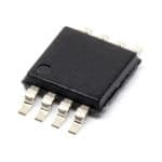
| 产品图片 |
|
| rohs | 符合RoHS无铅 / 符合限制有害物质指令(RoHS)规范要求 |
| 产品系列 | 数据转换器IC,数模转换器- DAC,Analog Devices AD5662BRMZ-1nanoDAC™ |
| 数据手册 | |
| 产品型号 | AD5662BRMZ-1 |
| 产品培训模块 | http://www.digikey.cn/PTM/IndividualPTM.page?site=cn&lang=zhs&ptm=19145http://www.digikey.cn/PTM/IndividualPTM.page?site=cn&lang=zhs&ptm=18614http://www.digikey.cn/PTM/IndividualPTM.page?site=cn&lang=zhs&ptm=26125http://www.digikey.cn/PTM/IndividualPTM.page?site=cn&lang=zhs&ptm=26140http://www.digikey.cn/PTM/IndividualPTM.page?site=cn&lang=zhs&ptm=26150http://www.digikey.cn/PTM/IndividualPTM.page?site=cn&lang=zhs&ptm=26147 |
| 产品种类 | 数模转换器- DAC |
| 位数 | 16 |
| 供应商器件封装 | 8-MSOP |
| 其它名称 | AD5662BRMZ1 |
| 分辨率 | 16 bit |
| 包装 | 管件 |
| 商标 | Analog Devices |
| 安装类型 | 表面贴装 |
| 安装风格 | SMD/SMT |
| 封装 | Tube |
| 封装/外壳 | 8-TSSOP,8-MSOP(0.118",3.00mm 宽) |
| 封装/箱体 | MSOP-8 |
| 工作温度 | -40°C ~ 125°C |
| 工厂包装数量 | 50 |
| 建立时间 | 8µs |
| 接口类型 | SPI |
| 数据接口 | SPI, DSP |
| 最大功率耗散 | 1.25 mW |
| 最大工作温度 | + 125 C |
| 最小工作温度 | - 40 C |
| 标准包装 | 50 |
| 电压参考 | External |
| 电压源 | 单电源 |
| 电源电压-最大 | 5.5 V |
| 电源电压-最小 | 2.7 V |
| 积分非线性 | +/- 16 LSB |
| 稳定时间 | 8 us |
| 系列 | AD5662 |
| 结构 | Resistor String |
| 设计资源 | |
| 转换器数 | 1 |
| 转换器数量 | 1 |
| 输出数和类型 | 1 电压 |
| 输出类型 | Voltage |
| 采样比 | 125 kSPs |
| 采样率(每秒) | - |


- 商务部:美国ITC正式对集成电路等产品启动337调查
- 曝三星4nm工艺存在良率问题 高通将骁龙8 Gen1或转产台积电
- 太阳诱电将投资9.5亿元在常州建新厂生产MLCC 预计2023年完工
- 英特尔发布欧洲新工厂建设计划 深化IDM 2.0 战略
- 台积电先进制程称霸业界 有大客户加持明年业绩稳了
- 达到5530亿美元!SIA预计今年全球半导体销售额将创下新高
- 英特尔拟将自动驾驶子公司Mobileye上市 估值或超500亿美元
- 三星加码芯片和SET,合并消费电子和移动部门,撤换高东真等 CEO
- 三星电子宣布重大人事变动 还合并消费电子和移动部门
- 海关总署:前11个月进口集成电路产品价值2.52万亿元 增长14.8%


PDF Datasheet 数据手册内容提取
2.7 V to 5.5 V, 250 μA, Rail-to-Rail Output 16-Bit nanoDACTM in a SOT-23 AD5662 FEATURES FUNCTIONAL BLOCK DIAGRAM Low power (250 μA @ 5 V) single 16-bit nanoDAC VREF GND VDD 12-bit accuracy guaranteed Tiny 8-lead SOT-23/MSOP package POWER-ON AD5662 Power-down to 480 nA @ 5 V, 100 nA @ 3 V RESET VFB Power-on reset to zero scale/midscale REF(+) 2.7 V to 5.5 V power supply REGDIASCTER 16-BIT OBUUFTFPEURT VOUT DAC Guaranteed 16-bit monotonic by design 3 power-down functions Serial interface with Schmitt-triggered inputs INPUT Rail-to-rail operation COLONTGRICOL CPOONWTREORL-D LOOWGNIC NREETSWISOTORRK SYNC interrupt facility TQeumalpifeieradt fuorre a ruatnogme o−t4iv0e°C a tpop +li1ca2t5i°oCn s 04777-001 APPLICATIONS SYNC SCLK DIN Process control Figure 1. Data acquisition systems Portable battery-powered instruments Digital gain and offset adjustment Programmable voltage and current sources Programmable attenuators GENERAL DESCRIPTION The AD5662, a member of the nanoDAC family, is a low power, The AD5662 uses a versatile 3-wire serial interface that operates single, 16-bit buffered voltage-out DAC that operates from a at clock rates up to 30 MHz, and is compatible with standard single 2.7 V to 5.5 V supply and is guaranteed monotonic by SPI®, QSPI™, MICROWIRE™, and DSP interface standards. design. PRODUCT HIGHLIGHTS The AD5662 requires an external reference voltage to set the output range of the DAC. The part incorporates a power-on 1. 16-bit DAC—12-bit accuracy guaranteed. reset circuit that ensures the DAC output powers up to 0 V (AD5662x-1) or to midscale (AD5662x-2), and remains there 2. Available in 8-lead SOT-23 and 8-lead MSOP packages. until a valid write takes place. The part contains a power-down 3. Low power. Typically consumes 0.42 mW at 3 V and feature that reduces the current consumption of the device to 0.75 mW at 5 V. 480 nA at 5 V and provides software-selectable output loads while in power-down mode. 4. Power-on reset to zero scale or to midscale. The low power consumption of this part in normal operation 5. 10 μs max settling time. makes it ideally suited to portable battery-operated equipment. The power consumption is 0.75 mW at 5 V, going down to RELATED DEVICES 2.4 μW in power-down mode. Part No. Description The AD5662’s on-chip precision output amplifier allows rail-to- AD5620/AD5640/AD5660 3 V/5 V 12-/14-/16-bit DAC with rail output swing to be achieved. For remote sensing applications, internal reference in SOT-23 the output amplifier’s inverting input is available to the user. Rev. A Information furnished by Analog Devices is believed to be accurate and reliable. However, no responsibility is assumed by Analog Devices for its use, nor for any infringements of patents or other rights of third parties that may result from its use. One Technology Way, P.O. Box 9106, Norwood, MA 02062-9106, U.S.A. Specifications subject to change without notice. No license is granted by implication or otherwise under any patent or patent rights of Analog Devices. Trademarks and Tel: 781.329.4700 www.analog.com registered trademarks are the property of their respective owners. Fax: 781.326.8703 ©2005–2010 Analog Devices, Inc. All rights reserved.
AD5662 TABLE OF CONTENTS Specifications.....................................................................................3 Power-On Reset..........................................................................15 Timing Characteristics.....................................................................5 Power-Down Modes..................................................................16 Absolute Maximum Ratings............................................................6 Microprocessor Interfacing......................................................16 ESD Caution..................................................................................6 Applications.....................................................................................18 Pin Configuration and Function Description..............................7 Choosing a Reference for the AD5662....................................18 Typical Performance Characteristics.............................................8 Using a Reference as a Power Supply for the AD5662..........18 Terminology....................................................................................13 Bipolar Operation Using the AD5662.....................................19 Theory of Operation......................................................................14 Using the AD5662 as an Isolated, Programmable, 4-20 mA Process Controller......................................................................19 DAC Section................................................................................14 Using AD5662 with a Galvanically Isolated Interface...........20 Resistor String.............................................................................14 Power Supply Bypassing and Grounding................................20 Output Amplifier........................................................................14 Outline Dimensions.......................................................................21 Serial Interface............................................................................14 Ordering Guide..........................................................................22 Input Shift Register....................................................................15 Automotive Products.................................................................22 SYNC Interrupt..........................................................................15 REVISION HISTORY 12/10—Rev. 0 to Rev. A Changes to Features Section.............................................................1 Changes to Ordering Guide...........................................................22 Added Automotive Products Section...........................................22 1/05—Revision 0: Initial Version Rev. A | Page 2 of 24
AD5662 SPECIFICATIONS V = 2.7 V to 5.5 V; R = 2 kΩ to GND; C = 200 pF to GND; V = V ; all specifications T to T , unless otherwise noted. DD L L REF DD MIN MAX Table 1. A Grade B Grade Y Version1 Parameter Min Typ Max Min Typ Max Unit Conditions/Comments STATIC PERFORMANCE2 Resolution 16 16 Bits Relative Accuracy ±8 ±32 ±8 ±16 LSB See Figure 4 Differential Nonlinearity ±1 ±1 LSB Guaranteed monotonic by design See Figure 5 Zero Code Error 2 10 2 10 mV All 0s loaded to DAC register Full-Scale Error −0.2 −1 −0.2 −1 % FSR All 1s loaded to DAC register Offset Error ±10 ±10 mV Gain Error ±1.5 ±1.5 % FSR Zero Code Error Drift3 ±2 ±2 μV/°C Gain Temperature Coefficient3 ±2.5 ±2.5 ppm Of FSR/°C DC Power Supply Rejection Ratio3 −100 −100 dB DAC code = midscale; V = 5 V/3 V ±10% DD OUTPUT CHARACTERISTICS3 Output Voltage Range 0 V 0 V V DD DD Output Voltage Settling Time 8 10 8 10 μs ¼ to ¾ scale change settling to ±2 LSB R = 2 kΩ; 0 pF < C < 200 pF L L Slew Rate 1.5 1.5 V/μs ¼ to ¾ scale Capacitive Load Stability 2 2 nF R = ∞ L 10 10 nF R = 2 kΩ L Output Noise Spectral Density4 100 100 nV/√Hz DAC code = midscale,10 kHz Output Noise (0.1 Hz to 10 Hz)4 10 10 μV p-p DAC code = midscale Total Harmonic Distortion (THD)4 −80 −80 dB V = 2 V ± 300 mV p-p, f = 5 kHz REF Digital-to-Analog Glitch Impulse 5 5 nV-s 1 LSB change around major carry Digital Feedthrough 0.1 0.1 nV-s DC Output Impedance 0.5 0.5 Ω Short-Circuit Current4 30 30 mA V = 5 V, 3 V DD Power-Up Time 4 4 μs Coming out of power-down mode V = 5 V, 3 V DD REFERENCE INPUT3 Reference Current 40 75 40 75 μA V = V = 5 V REF DD 30 50 30 50 μA V = V = 3.6 V REF DD Reference Input Range5 0.75 V 0.75 V V DD DD Reference Input Impedance 125 125 kΩ LOGIC INPUTS3 Input Current ±2 ±2 μA All digital inputs V , Input Low Voltage 0.8 0.8 V V = 5 V, 3 V INL DD V , Input High Voltage 2 2 V V = 5 V, 3 V INH DD Pin Capacitance 3 3 pF Rev. A | Page 3 of 24
AD5662 A Grade B Grade Y Version1 Parameter Min Typ Max Min Typ Max Unit Conditions/Comments POWER REQUIREMENTS V 2.7 5.5 2.7 5.5 V All digital inputs at 0 V or V DD DD I (Normal Mode) DAC active and excluding load current DD V = 4.5 V to 5.5 V 150 250 150 250 μA V = V and V = GND DD IH DD IL V = 2.7 V to 3.6 V 140 225 140 225 μA V = V and V = GND DD IH DD IL I (All Power-Down Modes) DD V = 4.5 V to 5.5 V 0.48 1 0.48 1 μA V = V and V = GND DD IH DD IL V = 2.7 V to 3.6 V 0.1 0.375 0.1 0.375 μA V = V and V = GND DD IH DD IL POWER EFFICIENCY I /I 90 90 % I = 2 mA. V = 5 V OUT DD LOAD DD 1 Temperature range is as follows: Y version: −40°C to +125°C, typical at +25°C. 2 DC specifications tested with the outputs unloaded, unless otherwise stated. Linearity calculated using a reduced code range of 512 to 65024. 3 Guaranteed by design and characterization; not production tested. 4 Output unloaded. 5 Reference input range at ambient where ±1 LSB max DNL specification is achievable. Rev. A | Page 4 of 24
AD5662 TIMING CHARACTERISTICS All input signals are specified with tr = tf = 1 ns/V (10% to 90% of V ) and timed from a voltage level of (V + V )/2. See Figure 2. DD IL IH V = 2.7 V to 5.5 V; all specifications T to T , unless otherwise noted. DD MIN MAX Table 2. Limit at T , T MIN MAX Parameter V = 2.7 V to 3.6 V V = 3.6 V to 5.5 V Unit Conditions/Comments DD DD t 1 50 33 ns min SCLK cycle time 1 t 13 13 ns min SCLK high time 2 t 13 13 ns min SCLK low time 3 t 13 13 ns min SYNC to SCLK falling edge setup time 4 t 5 5 ns min Data setup time 5 t 4.5 4.5 ns min Data hold time 6 t 0 0 ns min SCLK falling edge to SYNC rising edge 7 t 50 33 ns min Minimum SYNC high time 8 t 13 13 ns min SYNC rising edge to SCLK fall ignore 9 t 0 0 ns min SCLK falling edge to SYNC fall ignore 10 1 Maximum SCLK frequency is 30 MHz at VDD = 3.6 V to 5.5 V, and 20 MHz at VDD = 2.7 V to 3.6 V. t10 t1 t 9 SCLK t8 t4 t3 t2 t7 SYNC t 6 t DIN DB23 5 DB0 04777-002 Figure 2. Serial Write Operation Rev. A | Page 5 of 24
AD5662 ABSOLUTE MAXIMUM RATINGS T = 25°C, unless otherwise noted. A Table 3. Parameter Rating V to GND −0.3 V to +7 V Stresses above those listed under Absolute Maximum Ratings DD V to GND −0.3 V to V + 0.3 V may cause permanent damage to the device. This is a stress OUT DD V to GND −0.3 V to V + 0.3 V rating only; functional operation of the device at these or any FB DD V to GND −0.3 V to V + 0.3 V other conditions above those listed in the operational sections REF DD Digital Input Voltage to GND −0.3 V to V + 0.3 V of this specification is not implied. Exposure to absolute DD Operating Temperature Range maximum rating conditions for extended periods may affect Industrial (Y Version) −40°C to +125°C device reliability. Storage Temperature Range −65°C to +150°C Junction Temperature (T max) 150°C J Power Dissipation (T max − T )/θ J A JA SOT-23 Package (4-Layer Board) θ Thermal Impedance 119°C/W JA MSOP Package (4-Layer Board) θ Thermal Impedance 141°C/W JA θ Thermal Impedance 44°C/W JC Reflow Soldering Peak Temperature SnPb 240°C Pb-free 260°C ESD 2 kV ESD CAUTION ESD (electrostatic discharge) sensitive device. Electrostatic charges as high as 4000 V readily accumulate on the human body and test equipment and can discharge without detection. Although this product features proprietary ESD protection circuitry, permanent damage may occur on devices subjected to high energy electrostatic discharges. Therefore, proper ESD precautions are recommended to avoid performance degradation or loss of functionality. Rev. A | Page 6 of 24
AD5662 PIN CONFIGURATION AND FUNCTION DESCRIPTION VDD 1 8 GND VREF 2 AD5662 7 DIN TOP VIEW VFB 3 (Not to Scale) 6 SCLK VOUT 4 5 SYNC 04777-003 Figure 3. Pin Configuration Table 4. Pin Function Descriptions Pin No. Mnemonic Function 1 V Power Supply Input. These parts can be operated from 2.7 V to 5.5 V. V should be decoupled to GND. DD DD 2 V Reference Voltage Input. REF 3 V Feedback Connection for the Output Amplifier. V should be connected to V for normal operation. FB FB OUT 4 V Analog Output Voltage from DAC. The output amplifier has rail-to-rail operation. OUT 5 SYNC Level-Triggered Control Input (Active Low). This is the frame synchronization signal for the input data. When SYNC goes low, it enables the input shift register, and data is transferred in on the falling edges of the following clocks. The DAC is updated following the 24th clock cycle unless SYNC is taken high before this edge, in which case the rising edge of SYNC acts as an interrupt and the write sequence is ignored by the DAC. 6 SCLK Serial Clock Input. Data is clocked into the input shift register on the falling edge of the serial clock input. Data can be transferred at rates up to 30 MHz. 7 DIN Serial Data Input. This device has a 24-bit shift register. Data is clocked into the register on the falling edge of the serial clock input. 8 GND Ground Reference Point for All Circuitry on the Part. Rev. A | Page 7 of 24
AD5662 TYPICAL PERFORMANCE CHARACTERISTICS 10 8 VDD = VREF = 5V 8 TA = 25°C 6 MAX INL 6 VDD = VREF = 5V 4 4 OR (LSB) 02 R (LSB) 20 MAX DNL R O L ER –2 ERR –2 MIN DNL N I –4 –4 –6 MIN INL –1–80 04777-011 ––68 04777-036 0 5k 10k 15k 20k 25k 30k 35k 40k 45k 50k 55k 60k65k –40 –20 0 20 40 60 80 100 120 CODE TEMPERATURE (°C) Figure 7. INL Error and DNL Error vs. Temperature Figure 4. Typical INL Plot 10 8 MAX INL 6 VDD = 5V 4 TA = 25°C B) 2 S L MAX DNL R ( 0 O RR –2 MIN DNL E –4 –6 MIN INL –1–80 04777-045 0.75 1.25 1.75 2.25 2.75 3.25 3.75 4.25 4.75 VREF (V) Figure 5. Typical DNL Plot Figure 8. INL and DNL Error vs. VREF 90 8 VDD = VREF = 5V 80 TA = 25°C 6 MAX INL 70 TA = 25°C 4 60 OR (LSB) 50 R (LSB) 20 MAX DNL R 40 O ER ERR –2 MIN DNL 30 20 –4 MIN INL 100511 10511 20511 30511 40511 50511 60511 04777-019 ––68 04777-041 2.7 3.2 3.7 4.2 4.7 5.2 CODES VDD (V) Figure 6. Typical Total Unadjusted Error Plot Figure 9. INL and DNL Error vs. Supply Rev. A | Page 8 of 24
AD5662 0 1.0 VDD = 5V TA = 25°C –0.22 0.5 ZERO-SCALE ERROR –0.04 GAIN ERROR –0.06 0 SR) –0.08 V) F m –0.5 R (% –0.01 OR ( RRO –0.12 ERR –1.0 E –0.14 FULL-SCALE ERROR –1.5 –0.16 ––00..1280 04777-038 ––22..05 OFFSET ERROR 04777-039 –40 –20 0 20 40 60 80 100 120 2.7 3.2 3.7 4.2 4.7 5.2 TEMPERATURE (°C) VDD (V) Figure 10. Gain Error and Full-Scale Error vs. Temperature Figure 13. Zero-Scale and Offset Error vs. Supply 1.5 20 VDD = VREF = 5.5V 1.0 ZERO-SCALE ERROR 18 TA = 25°C 16 0.5 ES 14 mV) 0 EVIC 12 RROR ( –0.5 R OF D 10 E –1.0 BE 8 M U –1.5 N 6 OFFSET ERROR 4 ––22..05–40 –20 0 20 40 60 80 100 120 04777-035 20 04777-046 5 6 7 8 9 0 1 2 3 4 5 6 7 8 9 0 1 2 E TEMPERATURE (°C) 21 21 21 21 21 22 22 22 22 22 22 22 22 22 22 23 23 23 OR IDD (μA) M Figure 11. Zero-Scale and Offset Error vs. Temperature Figure 14. IDD Histogram with VDD = 5.5 V 1.0 0.20 VDD= VREF= 5V, 3V DAC LOADED WITH 0.5 0.15 TA = 25°C ZSEINRKOIN SGC ACLUERR–ENT GAIN ERROR 0.10 SR) 0 E (V) 0.05 F G RROR (% –0.5 FULL-SCALE ERROR R VOLTA –0.050 E –1.0 RO R –0.10 E –0.15 –1.5 –2.02.7 3.2 3.7 4.2 4.7 5.2 04777-042 ––00..2250 DFSUOALCUL RL SCOCIANADGLE ECDU– WRRITEHNT 04777-013 –5 –4 –3 –2 –1 0 1 2 3 4 5 VDD (V) I (mA) Figure 12. Gain Error and Full-Scale Error vs. Supply Figure 15. Headroom at Rails vs. Source and Sink Current Rev. A | Page 9 of 24
AD5662 250 1000 TA = 25°C VDD = VREF = 5V TA = 25°C 900 VDD = 5V 200 800 700 VDD = VREF = 3V 150 600 A) A) (μD (μD 500 D D I 100 I 400 300 50 200 0 04777-043 1000 VDD = 3V 04777-044 512 10512 20512 30512 40512 50512 60512 0 1 2 3 4 5 CODE VLOGIC (V) Figure 16. Supply Current vs. Code Figure 19. Supply Current vs. Logic Input Voltage 160 VDD =5V 140 VDD = VREF = 3V 120 VDD = 3V TFUA L=L 2-S5C°CALECODECHANGE 0x0000 TO 0xFFFF 100 OUTPUT LOADED WITH 2kΩ A) AND 200pF TO GND (μD 80 D I 60 VOUT= 455mV/DIV 40 200–40 –20 0 20 40 60 80 100 120 04777-037 TIME BASE = 4μs/DIV 04777-014 TEMPERATURE (°C) Figure 17. Supply Current vs. Temperature Figure 20. Full-Scale Settling Time, 3 V 160 TA = 25°C 140 120 VDD = VREF = 5V TA = 25°C 100 FULL-SCALECODECHANGE A) 0x0000 TO 0xFFFF (μD 80 OANUDTP 2U0T0 pLFO TAOD EGDN DWITH 2kΩ D I 60 VOUT= 909mV/DIV 40 1 2002.7 3.2 3.7 4.2 4.7 5.2 04777-040 TIME BASE = 4μs/DIV 04777-015 VDD (V) Figure 18. Supply Current vs. Supply Voltage Figure 21. Full-Scale Settling Time, 5 V Rev. A | Page 10 of 24
AD5662 2.502500 VTAD D= =2 5V°RCEF = 5V 22..550022205000 V1T3ADn D=S =2/S 5VA°RCMEFP L=E 5 VNUMBER 2.501750 1 LSB CHANGE AROUND MIDSCALE(0x8000TO0x7FFF) 2.501500 GLITCH IMPULSE = 2.723nV.s 2.501250 E2.501000 D TU2.500750 VDD MPLI2.500500 1 A2.500250 2.500000 MAX(C2)* 2.499750 420.0mV 2.499500 2 CH1 2.0VVOUTCH2 500mV M100μs 125MS/s 8.0ns/pt 04777-016 222...4449999982075050000 50 100 150 200 250 300 350 400 450 500 55004777-005 A CH1 1.28V SAMPLE NUMBER Figure 22. Power-On Reset to 0 V Figure 25. Digital-to-Analog Glitch Impulse (Negative) 2.500400 VDD = VREF = 5V TA = 25°C 2.500300 2.500200 2.500100 2.500000 VDD E2.499900 D 1 TU2.499800 PLI2.499700 M A2.499600 2.499500 VDD = VREF = 5V 2.499400 TA = 25°C 2 CH1 2.0VVOUTCH2 1.0V M100μs 125MS/s 8.0ns/pt 04777-017 222...444999999321000000 11G3 LMLnISITSDBC/SS HCCA HIAMMALPPNELUGE(L0E SNx A7EUFR M=FO BF1UE.2TNR7OD1n0Vx8.s000) 04777-006 A CH1 1.28V 0 50 100 150 200 250 300 350 400 450 500 550 SAMPLE NUMBER Figure 23. Power-On Reset to Midscale Figure 26. Digital-to-Analog Glitch Impulse (Positive) 2.500250 VDD = VREF = 5V 2.500200 TA = 25°C 2.500150 20nS/SAMPLE NUMBER DAC LOADED WITH MIDSCALE 2.500100 DIGITAL FEEDTHROUGH = 0.06nV.s 2.500050 SCLK DE2.500000 1 TU2.499950 PLI2.499900 M A2.499850 2.499800 2.499750 2 CH1 2.0VVOUTCH2 1.0V M1.0μs 5.0gS/s 200ps/pt 04777-018 222...4449999997660500000 50 100 150 200 250 300 350 400 450 500 55004777-007 A CH2 2.16V SAMPLE NUMBER Figure 24. Exiting Power-Down to Midscale Figure 27. Digital Feedthrough Rev. A | Page 11 of 24
AD5662 –20 –30 VTDADA DC= = 2L 55O°VACDED WITH FULL SCALE VDTADA DC= = 2L 5VO°RACEDFE =D 5 WVITH MIDSCALE VREF = 2V± 0.3Vp-p –40 –50 dB –60 1 –70 –80 ––10900 2k 4k 6k 8k 10k04777-008 XY AAXXIISS == 42μs/VD/DIVIV 04777-010 Hz Figure 28. Total Harmonic Distortion Figure 30. 0.1 Hz to 10 Hz Output Noise Plot 16 800 VREF = VDD VDD = VREF = 5V TA = 25°C 700 TA = 25°C 14 VDD=3V Hz) 600 12 √ V/ 500 n E (s)μ 10 OISE ( 400 M N TI T 8 VDD=5V TPU 300 U O 200 6 4 04777-009 1000 04777-020 0 1 2 3 4 5 6 7 8 9 10 10 100 1k 10k 100k 1M CAPACITANCE (nF) FREQUENCY (Hz) Figure 29. Settling Time vs. Capacitive Load Figure 31. Noise Spectral Density Rev. A | Page 12 of 24
AD5662 TERMINOLOGY Relative Accuracy or Integral Nonlinearity (INL) Offset Error For the DAC, relative accuracy or integral nonlinearity is a Offset error is a measure of the difference between V (actual) OUT measurement of the maximum deviation, in LSBs, from a and V (ideal) expressed in mV in the linear region of the OUT straight line passing through the endpoints of the DAC transfer transfer function. Offset error is measured on the AD5662 with function. A typical INL vs. code plot can be seen in Figure 4. Code 512 loaded in the DAC register. It can be negative or positive. Differential Nonlinearity (DNL) DC Power Supply Rejection Ratio (PSRR) Differential nonlinearity is the difference between the measured This indicates how the output of the DAC is affected by changes change and the ideal 1 LSB change between any two adjacent in the supply voltage. PSRR is the ratio of the change in VOUT to a codes. A specified differential nonlinearity of ±1 LSB maximum change in VDD for full-scale output of the DAC. It is measured in ensures monotonicity. This DAC is guaranteed monotonic by dB. VREF is held at 2 V, and VDD is varied by ±10%. design. A typical DNL vs. code plot can be seen in Figure 5. Output Voltage Settling Time This is the amount of time it takes for the output of a DAC to settle Zero-Code Error to a specified level for a ¼ to ¾ full-scale input change and is Zero-code error is a measurement of the output error when measured from the 24th falling edge of SCLK. zero code (0x0000) is loaded to the DAC register. Ideally, the output should be 0 V. The zero-code error is always positive in Digital-to-Analog Glitch Impulse the AD5662 because the output of the DAC cannot go below Digital-to-analog glitch impulse is the impulse injected into the 0 V. It is due to a combination of the offset errors in the DAC analog output when the input code in the DAC register changes and the output amplifier. Zero-code error is expressed in mV. A state. It is normally specified as the area of the glitch in nV-s, plot of zero-code error vs. temperature can be seen in Figure 11. and is measured when the digital input code is changed by 1 LSB at the major carry transition (0x7FFF to 0x8000). See Full-Scale Error Figure 25 and Figure 26. Full-scale error is a measurement of the output error when full- scale code (0xFFFF) is loaded to the DAC register. Ideally, the Digital Feedthrough output should be VDD − 1 LSB. Full-scale error is expressed in Digital feedthrough is a measure of the impulse injected into percent of full-scale range. A plot of full-scale error vs. the analog output of the DAC from the digital inputs of the temperature can be seen in Figure 10. DAC, but is measured when the DAC output is not updated. It is specified in nV-s, and measured with a full-scale code change Gain Error on the data bus, that is, from all 0s to all 1s and vice versa. This is a measure of the span error of the DAC. It is the deviation in slope of the DAC transfer characteristic from ideal expressed Total Harmonic Distortion (THD) as a percent of the full-scale range. This is the difference between an ideal sine wave and its attenuated version using the DAC. The sine wave is used as the reference for Total Unadjusted Error (TUE) the DAC, and the THD is a measurement of the harmonics present Total unadjusted error is a measurement of the output error, on the DAC output. It is measured in dB. taking all the various errors into account. A typical TUE vs. code plot can be seen in Figure 6. Noise Spectral Density This is a measurement of the internally generated random noise. Zero-Code Error Drift Random noise is characterized as a spectral density (voltage per This is a measurement of the change in zero-code error with a √Hz). It is measured by loading the DAC to midscale and meas- change in temperature. It is expressed in μV/°C. uring noise at the output. It is measured in nV/√Hz. A plot of noise spectral density can be seen in Figure 31. Gain Temperature Coefficient This is a measurement of the change in gain error with changes in temperature. It is expressed in (ppm of full-scale range)/°C. Rev. A | Page 13 of 24
AD5662 THEORY OF OPERATION DAC SECTION OUTPUT AMPLIFIER The AD5662 DAC is fabricated on a CMOS process. The The output buffer amplifier can generate rail-to-rail voltages on architecture consists of a string DAC followed by an output its output, which gives an output range of 0 V to V . This output DD buffer amplifier. Figure 32 shows a block diagram of the DAC buffer amplifier has a gain of 2 derived from a 50 kΩ resistor architecture. divider network in the feedback path. The output amplifier’s inverting input is available to the user, allowing for remote VDD R VFB sensing. This VFB pin must be connected to VOUT for normal R operation. It can drive a load of 2 kΩ in parallel with 1000 pF to REF (+) GND. The source and sink capabilities of the output amplifier can RESISTOR DAC REGISTER STRING VOUT be seen in Figure 15. The slew rate is 1.5 V/μs with a ¼ to ¾ REF ((cid:1)–) OUTPUT full-scale settling time of 10 μs. GND AMPLIFIER 04777-022 SERIAL INTERFACE The AD5662 has a 3-wire serial interface (SYNC, SCLK, and Figure 32. DAC Architecture DIN) that is compatible with SPI, QSPI, and MICROWIRE interface standards as well as with most DSPs. See Figure 2 for Since the input coding to the DAC is straight binary, the ideal a timing diagram of a typical write sequence. output voltage is given by The write sequence begins by bringing the SYNC line low. Data ⎛ D ⎞ VOUT =VREF×⎜⎝65,536⎟⎠ from the DIN line is clocked into the 24-bit shift register on the falling edge of SCLK. The serial clock frequency can be as high where D is the decimal equivalent of the binary code that is as 30 MHz, making the AD5662 compatible with high speed loaded to the DAC register. It can range from 0 to 65,535. DSPs. On the 24th falling clock edge, the last data bit is clocked in and the programmed function is executed, that is, a change RESISTOR STRING in DAC register contents and/or a change in the mode of opera- The resistor string section is shown in Figure 33. It is simply a tion. At this stage, the SYNC line can be kept low or be brought string of resistors, each of value R. The code loaded to the DAC high. In either case, it must be brought high for a minimum of register determines at which node on the string the voltage is 33 ns before the next write sequence so that a falling edge of tapped off to be fed into the output amplifier. The voltage is SYNC can initiate the next write sequence. Since the SYNC tapped off by closing one of the switches connecting the string buffer draws more current when V = 2.4 V than it does when IN to the amplifier. Because it is a string of resistors, it is guaranteed V = 0.8 V, SYNC should be idled low between write sequences IN monotonic. for even lower power operation. As mentioned previously it must, however, be brought high again just before the next write sequence. R R R TO OUTPUT AMPLIFIER R R 04777-023 Figure 33. Resistor String Rev. A | Page 14 of 24
AD5662 INPUT SHIFT REGISTER 24th falling edge, this acts as an interrupt to the write sequence. The shift register is reset and the write sequence is seen as The input shift register is 24 bits wide (see Figure 34). The first invalid. Neither an update of the DAC register contents nor a six bits are don’t cares. The next two are control bits that control change in the operating mode occurs (see Figure 35). the part’s mode of operation (normal mode or any one of three power-down modes). See the Power-Down Modes section for a POWER-ON RESET more complete description of the various modes. The next 16 The AD5662 family contains a power-on reset circuit that bits are the data bits. These are transferred to the DAC register controls the output voltage during power-up. The AD5662x-1 on the 24th falling edge of SCLK. DAC output powers up to 0 V, and the AD5662x-2 DAC output SYNC INTERRUPT powers up to midscale. The output remains there until a valid write sequence is made to the DAC. This is useful in In a normal write sequence, the SYNC line is kept low for at applications where it is important to know the state of the least 24 falling edges of SCLK, and the DAC is updated on the output of the DAC while it is in the process of powering up. 24th falling edge. However, if SYNC is brought high before the DB23 (MSB) DBO (LSB) X X X X X X PD1 PD0 D15 D14 D13 D12 D11 D10 D9 D8 D7 D6 D5 D4 D3 D2 D1 D0 DATA BITS 0 0 NORMAL OPERATION 0 1 1 kΩ TO GND 11 01 1T0H0R kEΩE -TSOT AGTNED POWER-DOWN MODES 04777-024 Figure 34. Input Register Contents SCLK SYNC DIN DB23 DB0 DB23 DB0 SYNC HINIGVAHL BIDE FWORRIETE 2 4STEHQ FUAELNLICNEG: EDGE VALID WORNIT ET HSEE Q24UTEH NFCAEL,L OINUGT PEUDTG EUPDATES 04777-025 Figure 35. SYNC Interrupt Facility Rev. A | Page 15 of 24
AD5662 POWER-DOWN MODES MICROPROCESSOR INTERFACING The AD5662 contains four separate modes of operation. These AD5662 to Blackfin® ADSP-BF53x Interface modes are software-programmable by setting two bits (DB17 and DB16) in the control register. Table 5 shows how the state Figure 37 shows a serial interface between the AD5662 and of the bits corresponds to the device’s mode of operation. the Blackfin ADSP-BF53x microprocessor. The ADSP-BF53x processor family incorporates two dual-channel synchronous Table 5. Modes of Operation for the AD5662 serial ports, SPORT1 and SPORT0, for serial and multiprocessor DB17 DB16 Operating Mode communications. Using SPORT0 to connect to the AD5662, the 0 0 Normal Operation setup for the interface is as follows. DT0PRI drives the DIN pin Power-Down Modes of the AD5662, while TSCLK0 drives the SCLK of the part. The 0 1 1 kΩ to GND SYNC is driven from TFS0. 1 0 100 kΩ to GND 1 1 Three-State ADSP-BF53x* AD5662* When both bits are set to 0, the part works normally with its TFS0 SYNC normal power consumption of 250 μA at 5 V. However, for the DTOPRI DIN three power-down modes, the supply current falls to 480 nA at 5th Ve o(1u0tp0u nt Ast aagt e3 iVs a).l sNoo itn otenrlnya dlloye ssw tihtec hseudp pfrlyo mcu trhree notu ftapllu, tb ouft TSCLK0 SCLK 04777-027 *ADDITIONAL PINS OMITTED FOR CLARITY the amplifier to a resistor network of known values. This has the advantage that the output impedance of the part is known while Figure 37. AD5662 to Blackfin ADSP-BF53x Interface the part is in power-down mode. The outputs can either be connected internally to GND through a 1 kΩ or 100 kΩ AD5662 to 68HC11/68L11 Interface resistor, or left open-circuited (three-state) (see Figure 36). Figure 38 shows a serial interface between the AD5662 and the 68HC11/68L11 microcontroller. SCK of the 68HC11/68L11 SRTERSINISGTDOARC AMPLIFIER VOUT drives the SCLK of the AD5662, while the MOSI output drives the serial data line of the DAC. The SYNC signal is derived from a port line (PC7). The setup POWER-DOWN conditions for correct operation of this interface are as follows. CIRCUITRY RESISTOR NETWORK 04777-026 Titsh Ce 6P8HHAC b1i1t /a6s8 aL 111. Wis hceonn fdigautar eisd bweiitnhg i ttrs aCnPsmOiLtt bedit taos tah 0e aDnAdC , the SYNC line is taken low (PC7). When the 68HC11/ 68L11 is Figure 36. Output Stage During Power-Down configured as described above, data appearing on the MOSI The bias generator, the output amplifier, the resistor string, and output is valid on the falling edge of SCK. Serial data from the other associated linear circuitry are shut down when power- 68HC11/68L11 is transmitted in 8-bit bytes with only eight down mode is activated. However, the contents of the DAC falling clock edges occurring in the transmit cycle. Data is register are unaffected when in power-down. The time to exit transmitted MSB first. In order to load data to the AD5662, PC7 power-down is typically 4 μs for V = 5 V and for V = 3 V DD DD is left low after the first eight bits are transferred, and a second (see Figure 24). serial write operation is performed to the DAC; PC7 is taken high at the end of this procedure. 68HC11/68L11* AD5662* PC7 SYNC SCK SCLK MOSI DIN 04777-028 *ADDITIONAL PINS OMITTED FOR CLARITY Figure 38. AD5662 to 68HC11/68L11 Interface Rev. A | Page 16 of 24
AD5662 AD5662 to 80C51/80L51 Interface AD5662 to MICROWIRE Interface Figure 39 shows a serial interface between the AD5662 and the Figure 40 shows an interface between the AD5662 and any 80C51/80L51 microcontroller. The setup for the interface is as MICROWIRE-compatible device. Serial data is shifted out on follows. TxD of the 80C51/80L51 drives SCLK of the AD5662, the falling edge of the serial clock and is clocked into the AD5662 while RxD drives the serial data line of the part. The SYNC on the rising edge of the SK. signal is again derived from a bit-programmable pin on the port. In this case, port line P3.3 is used. When data is to be transmitted MICROWIRE* AD5662* to the AD5662, P3.3 is taken low. The 80C51/80L51 transmits data in 8-bit bytes only; thus only eight falling clock edges occur CS SYNC in the transmit cycle. To load data to the DAC, P3.3 is left low SK SCLK aisf tienri ttihaete fdir tsot etrigahnts mbiitts tahree steracnonsmd ibttyetde ,o afn dda taa s. ePc3o.n3 dis w tarkiteen c ycle SO DIN 04777-030 high following the completion of this cycle. The 80C51/80L51 *ADDITIONAL PINS OMITTED FOR CLARITY outputs the serial data in a format that has the LSB first. The Figure 40. AD5662 to MICROWIRE Interface AD5662 must receive data with the MSB first. The 80C51/80L51 transmit routine should take this into account. 80C51/80L51* AD5662* P3.3 SYNC TxD SCLK RxD DIN 04777-029 *ADDITIONAL PINS OMITTED FOR CLARITY Figure 39. AD5662 to 80C51/80L51 Interface Rev. A | Page 17 of 24
AD5662 APPLICATIONS CHOOSING A REFERENCE FOR THE AD5662 USING A REFERENCE AS A POWER SUPPLY FOR THE AD5662 To achieve the optimum performance from the AD5662, thought should be given to the choice of a precision voltage Because the supply current required by the AD5662 is extremely reference. The AD5662 has only one reference input, V . The low, an alternative option is to use a voltage reference to supply REF voltage on the reference input is used to supply the positive the required voltage to the part (see Figure 41). This is especially input to the DAC. Therefore any error in the reference is useful if the power supply is quite noisy, or if the system supply reflected in the DAC. voltages are at some value other than 5 V or 3 V, for example, 15 V. The voltage reference outputs a steady supply voltage for When choosing a voltage reference for high accuracy applica- the AD5662; see Table 6 for a suitable reference. If the low drop- tions, the sources of error are initial accuracy, ppm drift, long- out REF195 is used, it must supply 250 μA of current to the term drift, and output voltage noise. Initial accuracy on the AD5662, with no load on the output of the DAC. When the output voltage of the DAC leads to a full-scale error in the DAC output is loaded, the REF195 also needs to supply the DAC. To minimize these errors, a reference with high initial current to the load. The total current required (with a 5 kΩ accuracy is preferred. Also, choosing a reference with an output load on the DAC output) is trim adjustment, such as the ADR423, allows a system designer to trim system errors out by setting a reference voltage to a 250 μA + (5 V/5 kΩ) = 1.25 mA voltage other than the nominal. The trim adjustment can also be used at temperature to trim out any error. The load regulation of the REF195 is typically 2 ppm/mA, which results in a 2.5 ppm (12.5 μV) error for the 1.25 mA Long-term drift is a measurement of how much the reference current drawn from it. This corresponds to a 0.164 LSB error. drifts over time. A reference with a tight long-term drift specification ensures that the overall solution remains relatively +15V stable during its entire lifetime. +5V REF195 The temperature coefficient of a reference’s output voltage 250μA effect INL, DNL, and TUE. A reference with a tight temperature coefficient specification should be chosen to reduce temperature 3-WIRE SYNC VDD VREF VOUT = 0V TO 5V dependence of the DAC output voltage in ambient conditions. SERIAL SCLK AD5662 INTERFACE Ibnu dhgigeht, arecfceurreanccye aopuptlpicuatt vioonltsa, gwe hniochis eh anveee das r etola btiev ecloyn lsoiwde nreodis. eI t DIN 04777-031 is important to choose a reference with as low an output noise Figure 41. REF195 as Power Supply to the AD5662 voltage as practical for the system noise resolution required. Precision voltage references such as the ADR425 produce low output noise in the 0.1 Hz to10 Hz range. Examples of recom- mended precision references for use as supply to the AD5662 are shown in the Table 6. Table 6. Partial List of Precision References for Use with the AD5662 Part No. Initial Accuracy (mV max) Temp Drift (ppmoC max) 0.1 Hz to 10 Hz Noise (μV p-p typ) V (V) OUT ADR425 ±2 3 3.4 5 ADR395 ±6 25 5 5 REF195 ±2 5 50 5 AD780 ±2 3 4 2.5/3 ADR423 ±2 3 3.4 3 Rev. A | Page 18 of 24
AD5662 BIPOLAR OPERATION USING THE AD5662 USING THE AD5662 AS AN ISOLATED, PROGRAMMABLE, 4-20 mA PROCESS The AD5662 has been designed for single-supply operation, CONTROLLER but a bipolar output range is also possible using the circuit in Figure 42. The circuit gives an output voltage range of ±5 V. In many process control system applications, 2-wire current Rail-to-rail operation at the amplifier output is achievable using transmitters are used to transmit analog signals through noisy an AD820 or an OP295 as the output amplifier. environments. These current transmitters use a zero-scale signal current of 4 mA that can power the transmitter’s signal The output voltage for any input code can be calculated as conditioning circuitry. The full-scale output signal in these follows: transmitters is 20 mA. The converse approach to process control can also be used; a low-power, programmable current VO =⎢⎡VDD×⎜⎛ D ⎟⎞×⎜⎛R1+R2⎟⎞−VDD×⎜⎛R2⎟⎞⎥⎤ source can be used to control remotely located sensors or ⎣ ⎝65,536⎠ ⎝ R1 ⎠ ⎝R1⎠⎦ devices in the loop. where D represents the input code in decimal (0 to 65,535). A circuit that performs this function is shown in Figure 43. With V = 5 V, R1 = R2 = 10 kΩ, Using the AD5662 as the controller, the circuit provides a DD programmable output current of 4 mA to 20 mA, proportional ⎛10×D⎞ to the DAC’s digital code. Biasing for the controller is provided V =⎜ ⎟−5V O ⎝65,536⎠ by the ADR02 and requires no external trim for two reasons: (1) the ADR02’s tight initial output voltage tolerance and (2) This is an output voltage range of ±5 V, with 0x0000 corre- the low supply current consumption of both the AD8627 and sponding to a −5 V output, and 0xFFFF corresponding to a the AD5662. The entire circuit, including opto-couplers, +5 V output. consumes less than 3 mA from the total budget of 4 mA. The AD8627 regulates the output current to satisfy the current R2 = 10kΩ summation at the noninverting node of the AD8627. +5V +5V R1 = 10kΩ I = 1/R7 (V × R3/R1 + V × R3/R2) OUT DAC REF AD820/ ±5V VFB OP295 For the values shown in Figure 43, VREF VOUT 10μF 0.1μF AD5662 –5V IOUT = 0.2435 μA × D + 4 mA where D = 0 ≤ D ≤ 65535, giving a full-scale output current of TINHTSREEERREFI-AWALCIREE 04777-032 2tr0im m aAt w4 hmeAn tihs ep rAoDvi5d6e6d2 b’sy d Pig2i,t aanl cdo Pd1e peqrouvailds e0sx tFhFeF cFi.r cOufifts’se t gain trim at 20 mA. These two trims do not interact because Figure 42. Bipolar Operation with the AD5662 the noninverting input of the AD8627 is at virtual ground. The Schottky diode, D1, is required in this circuit to prevent loop supply power-on transients from pulling the noninverting input of the AD8627 more than 300 mV below its inverting input. Without this diode, such transients could cause phase reversal of the AD8627 and possible latch-up of the controller. The loop supply voltage compliance of the circuit is limited by the maxi- mum applied input voltage to the ADR02 and is from 12 V to 40 V. ADR02 VLOOP R2 12V TO 36V 18.5kΩ P2 4mA ADJUST SELROIAADL AD5662 4.R7k1Ω A2D0PJmU1AST AD8627 3.R3k6Ω Q2N13904 R3 D1 4mA TO 20mA 1.5kΩ 100RΩ7 RL 04777-034 Figure 43. Programmable 4–20 mA Process Controller Rev. A | Page 19 of 24
AD5662 USING AD5662 WITH A POWER SUPPLY BYPASSING AND GROUNDING GALVANICALLY ISOLATED INTERFACE When accuracy is important in a circuit, it is helpful to carefully In process-control applications in industrial environments, it is consider the power supply and ground return layout on the often necessary to use a galvanically isolated interface to protect board. The printed circuit board containing the AD5662 should and isolate the controlling circuitry from any hazardous have separate analog and digital sections, each having its own common-mode voltages that might occur in the area where the area of the board. If the AD5662 is in a system where other DAC is functioning. Isocouplers provide isolation in excess of devices require an AGND-to-DGND connection, the connection 3 kV. The AD5662 uses a 3-wire serial logic interface, so the should be made at one point only. This ground point should be ADuM130x 3-channel digital isolator provides the required as close as possible to the AD5662. isolation (see Figure 44). The power supply to the part also The power supply to the AD5662 should be bypassed with 10 μF needs to be isolated, which is done by using a transformer. On and 0.1 μF capacitors. The capacitors should be located as close the DAC side of the transformer, a 5 V regulator provides the as possible to the device, with the 0.1 μF capacitor ideally right 5 V supply required for the AD5662. up against the device. The 10 μF capacitors are the tantalum +5V bead type. It is important that the 0.1 μF capacitor has low REGULATOR POWER 10μF 0.1μF effective series resistance (ESR) and effective series inductance (ESI), for example, common ceramic types of capacitors. This 0.1 μF capacitor provides a low impedance path to ground for high frequencies caused by transient currents due to internal VDD logic switching. SCLK V1A SCLK ADMu103x AD5662 The power supply line itself should have as large a trace as possible to provide a low impedance path and to reduce glitch SDI V1B VOB SYNC VOUT effects on the supply line. Clocks and other fast switching digital signals should be shielded from other parts of the board by digital ground. Avoid crossover of digital and analog signals if possible. When traces cross on opposite sides of the board, DATA V1C VOC DIN ensure that they run at right angles to each other to reduce GND 04777-033 fteeechdtnhiqrouueg ihs tehffee mctsic trhorsotruigph t etchhen bioqaured w. Thheree b tehset cboomarpdo lnayenout t side of the board is dedicated to the ground plane only and the Figure 44. AD5662 with a Galvanically Isolated Interface signal traces are placed on the solder side. However, this is not always possible with a 2-layer board. Rev. A | Page 20 of 24
AD5662 OUTLINE DIMENSIONS 2.90 BSC 8 7 6 5 1.60 BSC 2.80 BSC 1 2 3 4 PIN1 INDICATOR 0.65 BSC 1.95 1.30 BSC 1.15 0.90 1.45 MAX 0.22 0.08 0.60 0.15 MAX 00..3282 SEATING 84°° 00..4350 PLANE 0° COMPLIANT TO JEDEC STANDARDS MO-178BA Figure 45. 8-Lead SOT-23 (RJ-8) Dimensions shown in millimeters 3.00 BSC 8 5 3.00 4.90 BSC BSC 4 PIN 1 0.65 BSC 0.15 1.10 MAX 0.00 0.80 0.38 0.23 8° 0.60 0.22 0.08 0° 0.40 COPLANARITY SEATING 0.10 PLANE COMPLIANT TO JEDEC STANDARDS MO-187AA Figure 46. 8-Lead Mini Small Outline Package [MSOP] (RM-8) Dimensions shown in millimeters Rev. A | Page 21 of 24
AD5662 ORDERING GUIDE Package Package Power-On Model1, 2 Temperature Range Description Option Branding Reset to Code Acurracy AD5662ARJ-1500RL7 −40°C to +125°C 8-lead SOT-23 RJ-8 D38 Zero ±32 LSB INL AD5662ARJZ-1500RL7 −40°C to +125°C 8-lead SOT-23 RJ-8 D9P Zero ±32 LSB INL AD5662ARJ-1REEL7 −40°C to +125°C 8-lead SOT-23 RJ-8 D38 Zero ±32 LSB INL AD5662ARJZ-1REEL7 −40°C to +125°C 8-lead SOT-23 RJ-8 D9P Zero ±32 LSB INL AD5662ARJ-2500RL7 −40°C to +125°C 8-lead SOT-23 RJ-8 D39 Midscale ±32 LSB INL AD5662ARJ-2REEL7 −40°C to +125°C 8-lead SOT-23 RJ-8 D39 Midscale ±32 LSB INL AD5662ARJZ-2REEL7 −40°C to +125°C 8-lead SOT-23 RJ-8 D9Q Midscale ±32 LSB INL AD5662ARM-1 −40°C to +125°C 8-lead MSOP RM-8 D38 Zero ±32 LSB INL AD5662ARMZ-1 −40°C to +125°C 8-lead MSOP RM-8 D9P Zero ±32 LSB INL AD5662ARM-1REEL7 −40°C to +125°C 8-lead MSOP RM-8 D38 Zero ±32 LSB INL AD5662ARMZ-1REEL7 −40°C to +125°C 8-lead MSOP RM-8 D9P Zero ±32 LSB INL AD5662BRJ-1500RL7 −40°C to +125°C 8-lead SOT-23 RJ-8 D36 Zero ±16 LSB INL AD5662BRJZ-1500RL7 −40°C to +125°C 8-lead SOT-23 RJ-8 D9T Zero ±16 LSB INL AD5662BRJ-1REEL7 −40°C to +125°C 8-lead SOT-23 RJ-8 D36 Zero ±16 LSB INL AD5662BRJZ-1REEL7 −40°C to +125°C 8-lead SOT-23 RJ-8 D9T Zero ±16 LSB INL AD5662BRJ-2500RL7 −40°C to +125°C 8-lead SOT-23 RJ-8 D37 Midscale ±16 LSB INL AD5662BRJZ-2500RL7 −40°C to +125°C 8-lead SOT-23 RJ-8 D9R Midscale ±16 LSB INL AD5662BRJ-2REEL7 −40°C to +125°C 8-lead SOT-23 RJ-8 D37 Midscale ±16 LSB INL AD5662BRJZ-2REEL7 −40°C to +125°C 8-lead SOT-23 RJ-8 D9R Midscale ±16 LSB INL AD5662BRM-1 −40°C to +125°C 8-lead MSOP RM-8 D36 Zero ±16 LSB INL AD5662BRMZ-1 −40°C to +125°C 8-lead MSOP RM-8 D9T Zero ±16 LSB INL AD5662BRM-1REEL7 −40°C to +125°C 8-lead MSOP RM-8 D36 Zero ±16 LSB INL AD5662BRMZ-1REEL7 −40°C to +125°C 8-lead MSOP RM-8 D9T Zero ±16 LSB INL AD5662WARMZ-1REEL7 −40°C to +125°C 8-lead MSOP RM-8 D9P Zero ±32 LSB INL EVAL-AD5662EBZ Evaluation Board 1 Z = RoHS Compliant Part. 2 W = Qualified for Automotive Applications. AUTOMOTIVE PRODUCTS The AD5662WARMZ-1REEL7 model is available with controlled manufacturing to support the quality and reliability requirements of automotive applications. Note that this automotive model may have specifications that differ from the commercial models; therefore, designers should review the Specifications section of this data sheet carefully. Only the automotive grade product shown is available for use in automotive applications. Contact your local Analog Devices, Inc., account representative for specific product ordering information and to obtain the specific Automotive Reliability report for this model. Rev. A | Page 22 of 24
AD5662 NOTES Rev. A | Page 23 of 24
AD5662 NOTES ©2005–2010 Analog Devices, Inc. All rights reserved. Trademarks and registered trademarks are the property of their respective owners. D04777–0–12/10(A) Rev. A | Page 24 of 24
Mouser Electronics Authorized Distributor Click to View Pricing, Inventory, Delivery & Lifecycle Information: A nalog Devices Inc.: AD5662BRJZ-1500RL7 AD5662ARJZ-1REEL7 AD5662ARJ-2500RL7 AD5662BRJ-1500RL7 AD5662BRJZ-2REEL7 AD5662BRJZ-1REEL7 AD5662WARMZ-1REEL7 AD5662ARMZ-1REEL7 AD5662ARJZ-2REEL7 AD5662ARMZ-1 AD5662BRJZ-2500RL7 AD5662BRMZ-1 AD5662ARJZ-1500RL7 AD5662BRMZ-1REEL7