ICGOO在线商城 > 集成电路(IC) > 数据采集 - 数模转换器 > AD5629RBRUZ-2
 Datasheet下载
- 型号: AD5629RBRUZ-2
- 制造商: Analog
- 库位|库存: xxxx|xxxx
- 要求:
| 数量阶梯 | 香港交货 | 国内含税 |
| +xxxx | $xxxx | ¥xxxx |
查看当月历史价格
查看今年历史价格
AD5629RBRUZ-2产品简介:
ICGOO电子元器件商城为您提供AD5629RBRUZ-2由Analog设计生产,在icgoo商城现货销售,并且可以通过原厂、代理商等渠道进行代购。 AD5629RBRUZ-2价格参考¥96.72-¥133.26。AnalogAD5629RBRUZ-2封装/规格:数据采集 - 数模转换器, 12 位 数模转换器 8 16-TSSOP。您可以下载AD5629RBRUZ-2参考资料、Datasheet数据手册功能说明书,资料中有AD5629RBRUZ-2 详细功能的应用电路图电压和使用方法及教程。
AD5629RBRUZ-2 是 Analog Devices Inc.(ADI)公司生产的一款 12 位、双通道、电压输出型数模转换器(DAC),内置 2.5V 基准源,采用 TSSOP 封装。该器件具有高精度、低功耗和小封装的特点,适用于多种需要精密模拟信号生成的场合。

其主要应用场景包括:

1. 工业自动化与控制系统:用于控制阀门、执行器或传感器校准,提供精确的模拟电压输出以调节设备运行状态。

2. 测试与测量设备:如信号发生器、校准仪器等,用于产生高精度的参考信号或测试信号。

3. 医疗设备:如便携式诊断仪器、生命体征监测设备中的信号调节模块,要求高稳定性和重复性。

4. 通信系统:在基站或光模块中用于偏置控制、激光驱动调节等。

5. 嵌入式系统与仪表:作为微控制器系统的外围 DAC,实现对模拟量的精确控制。

由于其集成度高、占用空间小,特别适合对尺寸和功耗有要求的应用场景。
| 参数 | 数值 |
| 产品目录 | 集成电路 (IC)半导体 |
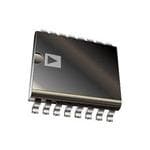
| 描述 | IC DAC 12BIT I2C/SRL 16TSSOP数模转换器- DAC Octal 12bit I2C w/125V/25V ref |
| DevelopmentKit | EVAL-AD5629RSDZ |
| 产品分类 | |
| 品牌 | Analog Devices Inc |
| 产品手册 | |
| 产品图片 |
|
| rohs | 符合RoHS无铅 / 符合限制有害物质指令(RoHS)规范要求 |
| 产品系列 | 数据转换器IC,数模转换器- DAC,Analog Devices AD5629RBRUZ-2denseDAC |
| 数据手册 | |
| 产品型号 | AD5629RBRUZ-2 |
| 产品培训模块 | http://www.digikey.cn/PTM/IndividualPTM.page?site=cn&lang=zhs&ptm=26125http://www.digikey.cn/PTM/IndividualPTM.page?site=cn&lang=zhs&ptm=26140http://www.digikey.cn/PTM/IndividualPTM.page?site=cn&lang=zhs&ptm=26150http://www.digikey.cn/PTM/IndividualPTM.page?site=cn&lang=zhs&ptm=26147 |
| 产品种类 | 数模转换器- DAC |
| 位数 | 12 |
| 供应商器件封装 | 16-TSSOP |
| 其它名称 | AD5629RBRUZ2 |
| 分辨率 | 12 bit |
| 包装 | 管件 |
| 商标 | Analog Devices |
| 安装类型 | 表面贴装 |
| 安装风格 | SMD/SMT |
| 封装 | Tube |
| 封装/外壳 | 16-TSSOP(0.173",4.40mm 宽) |
| 封装/箱体 | TSSOP-16 |
| 工作温度 | -40°C ~ 105°C |
| 工厂包装数量 | 96 |
| 建立时间 | 2.5µs |
| 接口类型 | Serial |
| 数据接口 | I²C |
| 最大工作温度 | + 105 C |
| 最小工作温度 | - 40 C |
| 标准包装 | 1 |
| 电压参考 | Internal, External |
| 电压源 | 单电源 |
| 电源电压-最大 | 5.5 V |
| 电源电压-最小 | 2.7 V |
| 积分非线性 | +/- 1 LSB |
| 稳定时间 | 6 us |
| 系列 | AD5629R |
| 结构 | Resistor String |
| 转换器数 | 8 |
| 转换器数量 | 8 |
| 输出数和类型 | 8 电压 |
| 输出类型 | Voltage |
| 采样比 | 166 kSPs |
| 采样率(每秒) | - |


- 商务部:美国ITC正式对集成电路等产品启动337调查
- 曝三星4nm工艺存在良率问题 高通将骁龙8 Gen1或转产台积电
- 太阳诱电将投资9.5亿元在常州建新厂生产MLCC 预计2023年完工
- 英特尔发布欧洲新工厂建设计划 深化IDM 2.0 战略
- 台积电先进制程称霸业界 有大客户加持明年业绩稳了
- 达到5530亿美元!SIA预计今年全球半导体销售额将创下新高
- 英特尔拟将自动驾驶子公司Mobileye上市 估值或超500亿美元
- 三星加码芯片和SET,合并消费电子和移动部门,撤换高东真等 CEO
- 三星电子宣布重大人事变动 还合并消费电子和移动部门
- 海关总署:前11个月进口集成电路产品价值2.52万亿元 增长14.8%


PDF Datasheet 数据手册内容提取
Octal, 12-/16-Bit, I2C, denseDACs with 5 ppm/°C On-Chip Reference Data Sheet AD5629R/AD5669R FEATURES FUNCTIONAL BLOCK DIAGRAM Low power octal DACs VDD VREFIN/VREFOUT AD5629R: 12 bits AD5629R/AD5669R 1.25V/2.5V REF AD5669R: 16 bits BUFFER 2.6 mm × 2.6 mm 16-ball WLCSP LDAC REINGPISUTTER REGDIASCTER SDTARCIN AG VOUTA 4 mm × 4 mm 16-lead LFCSP and 16-lead TSSOP SCL BUFFER On-chip 1.25 V/2.5 V, 5 ppm/°C reference REINGPISUTTER REGDIASCTER SDTARCIN BG VOUTB Power down to 400 nA at 5 V, 200 nA at 3 V BUFFER 2.7 V to 5.5 V power supply GIC REINGPISUTTER REGDIASCTER SDTARCIN CG VOUTC GPouwarearn-otene rde smeto tnoo ztoenroic s bcayl de eosri gmni dscale SDA ACE LO REINGPISUTTER REGDIASCTER SDTARCIN DG BUFFER VOUTD F 3 power-down functions ER BUFFER Hardware LDAC and CLR functions INT REINGPISUTTER REGDIASCTER SDTARCIN EG VOUTE I2C-compatible serial interface supports standard (100 kHz) BUFFER A0 and fast (400 kHz) modes REINGPISUTTER REGDIASCTER SDTARCIN FG VOUTF APPLICATIONS BUFFER Process control REINGPISUTTER REGDIASCTER SDTARCIN GG VOUTG BUFFER Data acquisition systems Portable battery-powered instruments REINGPISUTTER REGDIASCTER SDTARCIN HG VOUTH Digital gain and offset adjustment POWER-ON RESET POWER-DOWN LOGIC Programmable voltage and current sources LDACCLR GND 08819-001 Figure 1. GENERAL DESCRIPTION The AD5629R/AD5669R devices are low power, octal, 12-/16- The parts incorporate a power-on reset circuit to ensure that bit, buffered voltage-output DACs. All devices are guaranteed the DAC output powers up to 0 V (AD5629R-1/AD5629R-2, monotonic by design. AD5669R-1/AD5669R-2) or midscale (AD5629R-3/AD5669R-3) and remains powered up at this level until a valid write takes place. The AD5629R/AD5669R have an on-chip reference with an The part contains a power-down feature that reduces the current internal gain of 2. The AD5629R-1/AD5669R-1 have a 1.25 V, consumption of the device to 400 nA at 5 V and provides software- 5 ppm/°C reference, giving a full-scale output range of 2.5 V. selectable output loads while in power-down mode for any or The AD5629R-2/AD5629R-3 and the AD5669R-2/AD5669R-3 all DAC channels. have a 2.5 V 5 ppm/°C reference, giving a full-scale output range of 5 V depending on the option selected. Devices with 1.25 V PRODUCT HIGHLIGHTS reference selected operate from a single 2.7 V to 5.5 V supply. 1. Octal, 12-/16-bit DACs. Devices with 2.5 V reference selected operate from 4.5 V to 5.5 V. 2. On-chip 1.25 V/2.5 V, 5 ppm/°C reference. The on-chip reference is off at power-up, allowing the use of an 3. Available in 16-lead LFCSP and TSSOP, and 16-ball WLCSP. external reference. The internal reference is enabled via a 4. Power-on reset to 0 V or midscale. software write. 5. Power-down capability. When powered down, the DAC typically consumes 200 nA at 3 V and 400 nA at 5 V. Rev. F Document Feedback Information furnished by Analog Devices is believed to be accurate and reliable. However, no responsibility is assumed by Analog Devices for its use, nor for any infringements of patents or other One Technology Way, P.O. Box 9106, Norwood, MA 02062-9106, U.S.A. rights of third parties that may result from its use. Specifications subject to change without notice. No license is granted by implication or otherwise under any patent or patent rights of Analog Devices. Tel: 781.329.4700 ©2010–2018 Analog Devices, Inc. All rights reserved. Trademarks and registered trademarks are the property of their respective owners. Technical Support www.analog.com
AD5629R/AD5669R Data Sheet TABLE OF CONTENTS Features .............................................................................................. 1 Resistor String ............................................................................. 21 Applications ....................................................................................... 1 Internal Reference ...................................................................... 21 Functional Block Diagram .............................................................. 1 Output Amplifier ........................................................................ 22 General Description ......................................................................... 1 Serial Interface ............................................................................ 22 Product Highlights ........................................................................... 1 Write Operation.......................................................................... 22 Revision History ............................................................................... 2 Read Operation........................................................................... 22 Specifications ..................................................................................... 3 Input Shift Register .................................................................... 24 AC Characteristics ........................................................................ 6 Multiple Byte Operation ............................................................ 24 I2C Timing Characteristics .......................................................... 7 Internal Reference Register ....................................................... 25 Absolute Maximum Ratings ............................................................ 9 Power-On Reset .......................................................................... 25 ESD Caution .................................................................................. 9 Power-Down Modes .................................................................. 26 Pin Configurations and Function Descriptions ......................... 10 Clear Code Register ................................................................... 26 Typical Performance Characteristics ........................................... 12 LDAC Function .......................................................................... 28 Terminology .................................................................................... 19 Power Supply Bypassing and Grounding ................................ 28 Theory of Operation ...................................................................... 21 Outline Dimensions ....................................................................... 29 Digital-to-Analog Converter (DAC) Section ......................... 21 Ordering Guide .......................................................................... 30 REVISION HISTORY 6/2018—Rev. E to Rev. F 12/2010—Rev. 0 to Rev. A Changes to Serial Interface Section .............................................. 22 Changes to Features, General Description, and Product Updated Outline Dimensions ....................................................... 29 Highlights Sections............................................................................ 1 Changes to Ordering Guide .......................................................... 30 Changes to AD5629R Relative Accuracy Parameter, Reference Output (1.25 V) Reference Input Range Parameter, and Reference 9/2016—Rev. D to Rev. E Output (2.5 V) Reference Input Range Parameter (Table 1) ....... 3 Change to Read Operation Section .............................................. 22 Changes to Relative Accuracy Parameter, Reference Tempco Parameter (Table 2) ........................................................................... 5 4/2014—Rev. C to Rev. D Changes to Output Voltage Settling Time Parameter (Table 3) .. 6 Change to V B, V C, V D, V E, V G, V H Ball Changes to Table 5 ............................................................................. 9 OUT OUT OUT OUT OUT OUT Numbers; Table 6 ............................................................................ 11 Changes to CLR Pin Description (Table 6) ................................. 10 Added Figure 32 and Figure 33 .................................................... 15 2/2014—Rev. B to Rev. C Added Figure 46 ............................................................................. 17 Change to Table 6 ........................................................................... 11 Changes to Internal Reference Section ........................................ 20 Changes to Figure 38, Figure 39, and Figure 40 ......................... 17 Changes to Power-On Reset Section ........................................... 23 Changes to Ordering Guide .......................................................... 30 Changes to Clear Code Register Section ..................................... 24 Updated Outline Dimensions ....................................................... 27 2/2013—Rev. A to Rev. B Changes to Ordering Guide .......................................................... 28 Added 16-Ball WLCSP ....................................................... Universal Changes to Features Section............................................................ 1 10/2010—Revision 0: Initial Version Added Figure 5, Renumbered Sequentially ................................ 10 Moved Table 6 ................................................................................. 11 Changes to Figure 25 and Figure 26 ............................................. 15 Added Figure 58 .............................................................................. 29 Changes to Ordering Guide .......................................................... 30 Rev. F | Page 2 of 30
Data Sheet AD5629R/AD5669R SPECIFICATIONS V = 4.5 V to 5.5 V, R = 2 kΩ to GND, C = 200 pF to GND, V = V . All specifications T to T , unless otherwise noted. DD L L REFIN DD MIN MAX Table 1. A Grade1 B Grade1 Parameter Min Typ Max Min Typ Max Unit Test Conditions/Comments STATIC PERFORMANCE2 AD5629R Resolution 12 12 Bits Relative Accuracy ±0.5 ±4 ±0.5 ±1 LSB See Figure 7 Differential Nonlinearity ±0.25 ±0.25 LSB Guaranteed monotonic by design (see Figure 9) AD5669R Resolution 16 16 Bits Relative Accuracy ±8 ±32 ±8 ±16 LSB See Figure 6 Differential Nonlinearity ±1 ±1 LSB Guaranteed monotonic by design (see Figure 8) Zero-Code Error 6 19 6 19 mV All 0s loaded to DAC register (see Figure 19) Zero-Code Error Drift ±2 ±2 µV/°C Full-Scale Error −0.2 −1 −0.2 −1 % FSR All 1s loaded to DAC register (see Figure 20) Gain Error ±1 ±1 % FSR Gain Temperature Coefficient ±2.5 ±2.5 ppm Of FSR/°C Offset Error ±6 ±19 ±6 ±19 mV DC Power Supply Rejection –80 –80 dB V ± 10% DD Ratio DC Crosstalk 10 10 µV Due to full-scale output change, (External Reference) R = 2 kΩ to GND or V L DD 5 5 µV/mA Due to load current change 10 10 µV Due to powering down (per channel) DC Crosstalk 25 25 µV Due to full-scale output change, (Internal Reference) R = 2 kΩ to GND or V L DD 10 10 µV/mA Due to load current change OUTPUT CHARACTERISTICS3 Output Voltage Range 0 V 0 V V DD DD Capacitive Load Stability 2 2 nF R = ∞ L 10 10 nF R = 2 kΩ L DC Output Impedance 0.5 0.5 Ω Short-Circuit Current 30 30 mA V = 5 V DD Power-Up Time 4 4 µs Coming out of power-down mode, V = 5 V DD REFERENCE INPUTS Reference Current 40 50 40 50 µA V = V = 5.5 V (per DAC channel) REFIN DD Reference Input Range 0 V 0 V V DD DD Reference Input Impedance 14.6 14.6 kΩ REFERENCE OUTPUT (1.25 V) Output Voltage 1.247 1.253 1.247 1.253 µA T = 25°C A Reference Input Range ±15 ±5 ±15 ppm/°C LFCSP, TSSOP ±15 WLCSP Output Impedance 7.5 7.5 kΩ REFERENCE OUTPUT (2.5 V) Output Voltage 2.495 2.505 2.495 2.505 µA T = 25°C A Reference Input Range ±15 ±5 ±10 ppm/°C Output Impedance 7.5 7.5 kΩ Rev. F | Page 3 of 30
AD5629R/AD5669R Data Sheet A Grade1 B Grade1 Parameter Min Typ Max Min Typ Max Unit Test Conditions/Comments LOGIC INPUTS3 Input Current ±3 ±3 µA All digital inputs Input Low Voltage, V 0.8 0.8 V V = 5 V INL DD Input High Voltage, V 2 2 V V = 5 V INH DD Pin Capacitance 3 3 pF POWER REQUIREMENTS V 4.5 5.5 4.5 5.5 V All digital inputs at 0 or V , DD DD DAC active, excludes load current I (Normal Mode)4 V = V and V = GND DD IH DD IL V = 4.5 V to 5.5 V 1.3 1.8 1.3 1.8 mA Internal reference off DD 2 2.5 2 2.5 mA Internal reference on I (All Power-Down Modes)5 DD V = 4.5 V to 5.5 V 0.4 1 0.4 1 µA V = V and V = GND DD IH DD IL 1 Temperature range is −40°C to +105°C, typical at 25°C. 2 Linearity calculated using a reduced code range of the AD5629R (Code 32 to Code 4064) and the AD5669R (Code 512 to 65,024). Output unloaded. 3 Guaranteed by design and characterization; not production tested. 4 Interface inactive. All DACs active. DAC outputs unloaded. 5 All eight DACs powered down. Rev. F | Page 4 of 30
Data Sheet AD5629R/AD5669R V = 2.7 V to 3.6 V, R = 2 kΩ to GND, C = 200 pF to GND, V = V . All specifications T to T , unless otherwise noted. DD L L REFIN DD MIN MAX Table 2. A Grade1 B Grade1 Parameter Min Typ Max Min Typ Max Unit Conditions/Comments STATIC PERFORMANCE2 AD5629R Resolution 12 12 Bits Relative Accuracy ±0.5 ±4 ±0.5 ±1 LSB See Figure 7 Differential Nonlinearity ±0.25 ±0.25 LSB Guaranteed monotonic by design (see Figure 9) AD5669R Resolution 16 16 Bits Relative Accuracy ±8 ±32 ±8 ±16 LSB See Figure 6 Differential Nonlinearity ±1 ±1 LSB Guaranteed monotonic by design (see Figure 8) Zero-Code Error 6 19 6 19 mV All 0s loaded to DAC register (see Figure 19) Zero-Code Error Drift ±2 ±2 µV/°C Full-Scale Error −0.2 −1 −0.2 −1 % FSR All 1s loaded to DAC register (see Figure 20) Gain Error ±1 ±1 % FSR Gain Temperature Coefficient ±2.5 ±2.5 ppm Of FSR/°C Offset Error ±6 ±19 ±6 ±19 mV DC Power Supply Rejection –80 –80 dB V ± 10% DD Ratio DC Crosstalk 10 10 µV Due to full-scale output change, (External Reference) R = 2 kΩ to GND or V L DD 5 5 µV/mA Due to load current change 10 10 µV Due to powering down (per channel) DC Crosstalk 25 25 µV Due to full-scale output change, (Internal Reference) R = 2 kΩ to GND or V L DD 10 10 µV/mA Due to load current change OUTPUT CHARACTERISTICS3 Output Voltage Range 0 V 0 V V DD DD Capacitive Load Stability 2 2 nF R = ∞ L 10 10 nF R = 2 kΩ L DC Output Impedance 0.5 0.5 Ω Short-Circuit Current 30 30 mA V = 3 V DD Power-Up Time 4 4 µs Coming out of power-down mode, V = 3 V DD REFERENCE INPUTS Reference Current 40 50 40 50 µA V = V = 3.6 V (per DAC channel) REFIN DD Reference Input Range 0 V 0 V DD DD Reference Input Impedance 14.6 14.6 kΩ REFERENCE OUTPUT Output Voltage AD5629R/AD5669R 1.247 1.253 1.247 1.253 V T = 25°C A Reference Tempco3 ±15 ±5 ±15 ppm/°C LFCSP, TSSOP ±15 WLCSP Reference Output Impedance 7.5 7.5 kΩ LOGIC INPUTS3 Input Current ±3 ±3 µA All digital inputs Input Low Voltage, V 0.8 0.8 V V = 3 V INL DD Input High Voltage, V 2 2 V V = 3 V INH DD Pin Capacitance 3 3 pF Rev. F | Page 5 of 30
AD5629R/AD5669R Data Sheet A Grade1 B Grade1 Parameter Min Typ Max Min Typ Max Unit Conditions/Comments POWER REQUIREMENTS V 2.7 3.6 2.7 3.6 V All digital inputs at 0 or V , DD DD DAC active, excludes load current I (Normal Mode)4 V = V and V = GND DD IH DD IL V = 2.7 V to 3.6 V 1.0 1.5 1.0 1.5 mA Internal reference off DD 1.8 2.25 1.7 2.25 mA Internal reference on I (All Power-Down Modes)5 DD V = 2.7 V to 3.6 V 0.2 1 0.2 1 µA V = V and V = GND DD IH DD IL 1 Temperature range is −40°C to +105°C, typical at 25°C. 2 Linearity calculated using a reduced code range of the AD5629R (Code 32 to Code 4064) and the AD5669R (Code 512 to 65,024). Output unloaded. 3 Guaranteed by design and characterization; not production tested. 4 Interface inactive. All DACs active. DAC outputs unloaded. 5 All eight DACs powered down. AC CHARACTERISTICS V = 2.7 V to 5.5 V, R = 2 kΩ to GND, C = 200 pF to GND, V = V . All specifications T to T , unless otherwise noted. DD L L REFIN DD MIN MAX Table 3. Parameter1, 2 Min Typ Max Unit Conditions/Comments3 Output Voltage Settling Time 2.5 7 µs ¼ to ¾ scale settling to ±2 LSB Slew Rate 1.2 V/µs Digital-to-Analog Glitch Impulse 4 nV-s 1 LSB change around major carry (see Figure 35) 19 nV-s From Code 59904 to Code 59903 Digital Feedthrough 0.1 nV-s Reference Feedthrough −90 dB V = 2 V ± 0.1 V p-p, frequency = 10 Hz to 20 MHz REFIN Digital Crosstalk 0.2 nV-s Analog Crosstalk 0.4 nV-s DAC-to-DAC Crosstalk 0.8 nV-s Multiplying Bandwidth 320 kHz V = 2 V ± 0.2 V p-p REFIN Total Harmonic Distortion −80 dB V = 2 V ± 0.1 V p-p, frequency = 10 kHz REFIN Output Noise Spectral Density 120 nV/√Hz DAC code = 0x8400, 1 kHz 100 nV/√Hz DAC code = 0x8400, 10 kHz 1 Guaranteed by design and characterization; not production tested. 2 See the Terminology section. 3 Temperature range is −40°C to +105°C, typical at 25°C. Rev. F | Page 6 of 30
Data Sheet AD5629R/AD5669R I2C TIMING CHARACTERISTICS V = 2.7 V to 5.5 V; all specifications T to T , f = 400 kHz, unless otherwise noted. DD MIN MAX SCL Table 4. Parameter Conditions Min Max Unit Description f 1 Standard mode 100 kHz Serial clock frequency SCL Fast mode 400 kHz t Standard mode 4 μs t , SCL high time 1 HIGH Fast mode 0.6 μs t Standard mode 4.7 μs t , SCL low time 2 LOW Fast mode 1.3 μs t Standard mode 250 ns t , data setup time 3 SU;DAT Fast mode 100 ns t Standard mode 0 3.45 μs t , data hold time 4 HD;DAT Fast mode 0 0.9 μs t Standard mode 4.7 μs t , setup time for a repeated start condition 5 SU;STA Fast mode 0.6 μs t Standard mode 4 μs t , hold time (repeated) start condition 6 HD;STA Fast mode 0.6 μs t Standard mode 4.7 μs t , bus-free time between a stop and a start condition 7 BUF Fast mode 1.3 μs t Standard mode 4 μs t , setup time for a stop condition 8 SU;STO Fast mode 0.6 μs t Standard mode 1000 ns t , rise time of SDA signal 9 RDA Fast mode 300 ns t Standard mode 300 ns t , fall time of SDA signal 10 FDA Fast mode 300 ns t Standard mode 1000 ns t , rise time of SCL signal 11 RCL Fast mode 300 ns t Standard mode 1000 ns t , rise time of SCL signal after a repeated start condition and 11A RCL1 after an acknowledge bit Fast mode 300 ns t Standard mode 300 ns t , fall time of SCL signal 12 FCL Fast mode 300 ns t13 Standard mode 10 ns LDAC pulse width low Fast mode 10 ns t Standard mode 300 ns Falling edge of ninth SCL clock pulse of last byte of a valid write to 14 the LDAC falling edge Fast mode 300 ns t15 Standard mode 20 ns CLR pulse width low Fast mode 20 ns t 2 Fast mode 0 50 ns Pulse width of spike suppressed SP 1 The SDA and SCL timing is measured with the input filters enabled. Switching off the input filters improves the transfer rate but has a negative effect on the EMC behavior of the part. 2 Input filtering on the SCL and SDA inputs suppresses noise spikes that are less than 50 ns for fast mode or less than 10 ns for high speed mode. Rev. F | Page 7 of 30
AD5629R/AD5669R Data Sheet t11 t12 t6 t2 SCL t6 t1 t5 t8 t4 t3 t10 t9 SDA t7 P S S t14 P LDAC* t13 CLR *ASYNCHRONOUS LDAC UPDATE MODE. t15 08819-002 Figure 2. Serial Write Operation Rev. F | Page 8 of 30
Data Sheet AD5629R/AD5669R ABSOLUTE MAXIMUM RATINGS Stresses at or above those listed under Absolute Maximum T = 25°C, unless otherwise noted. A Ratings may cause permanent damage to the product. This is a Table 5. stress rating only; functional operation of the product at these Parameter Rating or any other conditions above those indicated in the operational V to GND −0.3 V to +7 V section of this specification is not implied. Operation beyond DD Digital Input Voltage to GND −0.3 V to V + 0.3 V the maximum operating conditions for extended periods may DD V to GND −0.3 V to V + 0.3 V affect product reliability. OUT DD V /V to GND −0.3 V to V + 0.3 V REFIN REFOUT DD Operating Temperature Range ESD CAUTION Industrial −40°C to +105°C Storage Temperature Range −65°C to +150°C Junction Temperature (T ) +150°C JMAX Power Dissipation (T − T )/θ JMAX A JA Thermal Impedance, θ JA 16-Lead TSSOP (4-Layer Board) 112.6°C/W 16-Lead LFCSP (4-Layer Board) 30.4°C/W Reflow Soldering Peak Temperature Pb Free 260°C Rev. F | Page 9 of 30
AD5629R/AD5669R Data Sheet PIN CONFIGURATIONS AND FUNCTION DESCRIPTIONS AD5629R/AD5669R C A L A 0 D C D A L S S 6 5 4 3 1 1 1 1 VDD 1 12 GND LDAC 1 16 SCL VOUTA 2 TOP VIEW 11 VOUTB A0 2 15 SDA VOUTC 3 (Not to Scale) 10 VOUTD VOUTE 4 9 VOUTF VOVUTDAD 34 AADD55662699RR/ 1143 GVONUDTB TOP VIEW 5 6 7 8 VOUTC 5 (Not to Scale) 12 VOUTD VGTUO VTUOFER RLC VHTUO VVOOUUTTGE 67 1110 VVOOUUTTHF N1.O ETXEPSOSED PAD V/MNFIERUST BE TIED TO GND. 08819-003 VREFIN/VREFOUT 8 9 CLR 08819-004 Figure 3. 16-Lead LFCSP (CP-16-17) Figure 4. 16-Lead TSSOP (RU-16) BALLA1 INDICATOR 1 2 3 4 GND SCL SDA A0 A VOUTB LDAC VDD VOUTA B VOUTFVOUTDVOUTEVOUTC C D VOUTH CLR VREF VOUTG 08819-105 TOP VIEW (BALL SIDE DOWN) Not to Scale Figure 5. 16-Ball WLCSP Rev. F | Page 10 of 30
Data Sheet AD5629R/AD5669R Table 6. Pin Function Descriptions Pin No. LFCSP TSSOP WLCSP Mnemonic Description 15 1 B2 LDAC Pulsing this pin low allows any or all DAC registers to be updated if the input registers have new data. This allows all DAC outputs to simultaneously update. Alternatively, this pin can be tied permanently low. 16 2 A4 A0 Address Input. Sets the least significant bit of the 7-bit slave address. 1 3 B3 V Power Supply Input. These parts can be operated from 2.7 V to 5.5 V. Decouple the DD supply with a 10 µF capacitor in parallel with a 0.1 µF capacitor to GND. 2 4 B4 V A Analog Output Voltage from DAC A. The output amplifier has rail-to-rail operation. OUT 3 5 C4 V C Analog Output Voltage from DAC C. The output amplifier has rail-to-rail operation. OUT 4 6 C3 V E Analog Output Voltage from DAC E. The output amplifier has rail-to-rail operation. OUT 5 7 D4 V G Analog Output Voltage from DAC G. The output amplifier has rail-to-rail operation. OUT 6 8 D3 V /V The AD5629R/AD5669R have a common pin for reference input and reference output. REFIN REFOUT When using the internal reference, this is the reference output pin. When using an external reference, this is the reference input pin. The default for this pin is as a reference input. 7 9 D2 CLR Asynchronous Clear Input. The CLR input is falling edge sensitive. When CLR is low, all LDAC pulses are ignored. When CLR is activated, the input register and the DAC register are updated with the data contained in the CLR code register—zero scale, midscale, or full scale. The default setting clears the output to 0 V. 8 10 D1 V H Analog Output Voltage from DAC H. The output amplifier has rail-to-rail operation. OUT 9 11 C1 V F Analog Output Voltage from DAC F. The output amplifier has rail-to-rail operation. OUT 10 12 C2 V D Analog Output Voltage from DAC D. The output amplifier has rail-to-rail operation. OUT 11 13 B1 V B Analog Output Voltage from DAC B. The output amplifier has rail-to-rail operation. OUT 12 14 A1 GND Ground Reference Point for All Circuitry on the Parts. 13 15 A3 SDA Serial Data Input. This is used in conjunction with the SCL line to clock data into or out of the 32-bit input shift register. It is a bidirectional, open-drain data line that should be pulled to the supply with an external pull-up resistor. 14 16 A2 SCL Serial Clock Line. This is used in conjunction with the SDA line to clock data into or out of the 32-bit input shift register. 17 N/A N/A Exposed Pad The exposed pad must be tied to GND. (EPAD) Rev. F | Page 11 of 30
AD5629R/AD5669R Data Sheet TYPICAL PERFORMANCE CHARACTERISTICS 10 0.20 VDD = 5V VDD = 5V 8 EXT REF = 5V EXT REF = 5V TA = 25°C 0.15 TA = 25°C 6 0.10 4 0.05 INL (LSB) –220 DNL (LSB)–0.050 –4 –0.10 –6 –0.15 –8 –100 10k 20k 3C0kODES 40k 50k 60k65535 08819-106 –0.200 500 1000 1500 C2O00D0ES2500 3000 3500 4095 08819-111 Figure 6. INL AD5669R—External Reference Figure 9. DNL AD5629R—External Reference 1.0 10 VDD = 5V VDD = 5V 0.8 EXT REF = 5V INT REF = 2.5V TA = 25°C TA = 25°C 0.6 5 0.4 B) 0.2 B) S S NL (L 0 NL (L 0 I –0.2 I –0.4 –5 –0.6 –0.8 –1.00 500 1000 1500 C2O00D0ES2500 3000 3500 4095 08819-108 –100 10k 20k 3C0kODES 40k 50k 60k65535 08819-112 Figure 7. INL AD5629R—External Reference Figure 10. INL AD5669R-2—Internal Reference 1.0 1.0 VDD = 5V VDD = 5V 0.8 EXT REF = 5V INT REF = 2.5V TA = 25°C TA = 25°C 0.6 0.5 0.4 DNL (LSB) –00..220 INL (LSB) 0 –0.4 –0.5 –0.6 –0.8 –1.00 10k 20k 3C0kODES 40k 50k 60k65535 08819-109 –1.00 500 1000 1500 C2O00D0ES2500 3000 3500 4095 08819-114 Figure 8. DNL AD5669R—External Reference Figure 11. INL AD5629R-2—Internal Reference Rev. F | Page 12 of 30
Data Sheet AD5629R/AD5669R 1.0 1.0 VDD = 5V VDD = 3V INT REF = 2.5V INT REF = 1.25V TA = 25°C TA = 25°C 0.5 0.5 B) B) NL (LS 0 NL (LS 0 D I –0.5 –0.5 –1.00 10k 20k 3C0kODES 40k 50k 60k65535 08819-115 –1.00 500 1000 1500 C2O00D0ES2500 3000 3500 4095 08819-120 Figure 12. DNL AD5669R-2—Internal Reference Figure 15. INL AD5629R-1—Internal Reference 0.20 1.0 VDD = 5V VDD = 3V INT REF = 2.5V INT REF = 1.25V 0.15 TA = 25°C TA = 25°C 0.10 0.5 0.05 B) B) DNL (LS 0 DNL (LS 0 –0.05 –0.10 –0.5 –0.15 –0.200 500 1000 1500 C2O00D0ES2500 3000 3500 4095 08819-117 –1.00 10k 20k 3C0kODES 40k 50k 60k65535 08819-121 Figure 13. DNL AD5629R-2—Internal Reference Figure 16. DNL AD5669R-1—Internal Reference 10 0.20 VDD = 3V VDD = 3V 8 INT REF = 1.25V INT REF = 1.25V TA = 25°C 0.15 TA = 25°C 6 0.10 4 B) 2 B) 0.05 S S L (L 0 L (L 0 N N I –2 D –0.05 –4 –0.10 –6 –0.15 –8 –100 10k 20k 3C0kODES 40k 50k 60k65535 08819-118 –0.200 500 1000 1500 C2O00D0ES2500 3000 3500 4095 08819-123 Figure 14. INL AD5669R-1—Internal Reference Figure 17. DNL AD5629R-1—Internal Reference Rev. F | Page 13 of 30
AD5629R/AD5669R Data Sheet 0 1.95 VDD = 5V TA = 25°C 1.90 –0.05 1.85 OFFSET ERROR SR)–0.10 V) 1.80 F m R (% –0.15 FULL-SCALE ERROR OR ( 1.75 O R R R ER–0.20 E 1.70 ZERO-CODE ERROR GAIN ERROR 1.65 –0.25 1.60 –0.30–40 –25 –10 5 T2E0MPE35RATU50RE (°6C5) 80 95 110 125 08819-124 1.552.7 3.1 3.5 3.9VDD (V4).3 4.7 5.1 5.5 08819-127 Figure 18. Gain Error and Full-Scale Error vs. Temperature Figure 21. Zero-Code Error and Offset Error vs. Supply Voltage 6 21 VDD = 5V 18 5 OFFSET ERROR 15 4 S OR (mV) 3 ZERO-CODE ERROR R OF HIT 12 RR BE 9 E M U 2 N 6 1 3 0–40 –25 –10 5 T2E0MPE35RATU50RE (°6C5) 80 95 110 125 08819-125 00.85 IDD0 .W90ITH EXTERN0A.9L5 REFERENCE1 .(0m0A) 1.05 08819-128 Figure 22. IDD Histogram with External Reference Figure 19. Zero-Code Error and Offset Error vs. Temperature 18 –0.16 –0.17 FULL-SCALE ERROR TA = 25°C 16 –0.18 14 –0.19 S 12 T R) HI ERROR (% FS–––000...222210 NUMBER OF 1086 –0.23 4 –0.24 GAIN ERROR 2 –0.25 0 –0.262.7 3.1 3.5 3.9VDD (V4).3 4.7 5.1 5.5 08819-126 1.65Figure 213.I7D.0 DID WDIT HHi sItN1oT.g7E5rRaNmA Lw RitEh1F .IE8nR0teErNnCaEl R(me1fA.e8)r5ence 1.90 08819-129 Figure 20. Gain Error and Full-Scale Error vs. Supply Voltage Rev. F | Page 14 of 30
Data Sheet AD5629R/AD5669R 0.4 1.8 TA = 25°C TA = 25°C 0.3 1.7 1.6 0.2 VDD = 5V V) 1.5 E ( 0.1 LTAG 0 VDD = 3V, INT REF = 1.25V mA) 1.4 VDD = 3V OR VO –0.1 I (DD 11..23 R R –0.2 E 1.1 –0.3 1.0 VDD = 5V, INT REF = 2.5V –0.4 0.9 –0.5–10 –8 –6 SO–4URCE–/2SINK 0CURR2ENT (m4A) 6 8 10 08819-130 0.80 10k 2D0IkGITAL 3C0OkDES (D4e0ckimal) 50k 60k 08819-133 Figure 24. Headroom at Rails vs. Source and Sink Figure 27. Supply Current vs. Code 6 2.0 VDD = 5V TA = 25°C INT REF = 2.5V FULL SCALE 1.9 5 TA = 25°C 1.8 4 3/4 SCALE 1.7 (V)OUT 3 MIDSCALE (mA)DD 11..56 VVDDDD == 35..65VV V 2 I 1.4 1/4 SCALE 1.3 1 1.2 0 ZERO CODE 1.1 ––10.03 –0.02 SOU–R0C.0E1AND SI0NK CURR0E.0N1T (A) 0.02 0.03 08819-131 1.0–40 –25 –10 5 T2E0MPE35RATU50RE (°6C5) 80 95 110 125 08819-134 Figure 25. AD5669R-2 Source and Sink Capability Figure 28. Supply Current vs. Temperature 4.0 VDD = 3V 1.48 TA = 25°C 3.5 INT REF = 1.25V TA = 25°C 1.46 3.0 FULL SCALE 1.44 2.5 (V)UT 12..50 MIDSCAL3E/4 SCALE (mA)D 1.42 VO ID 1.40 1.0 1/4 SCALE 0.5 1.38 ZERO CODE 0 1.36 –0.5 1.34 –1.–00.03 –0.02 SOU–R0C.0E1 AND SI0NK CURR0E.0N1T (A) 0.02 0.03 08819-132 2.7 3.1 3.5 3.9VDD (V4).3 4.7 5.1 5.5 08819-135 Figure 26. AD5669R-1 Source and Sink Capability Figure 29. Supply Current vs. Supply Voltage Rev. F | Page 15 of 30
AD5629R/AD5669R Data Sheet 2.3 5.5 TA = 25°C VDD = 5V 5.0 EXT REF = 5V 2.1 4.5 TA = 25°C 1.9 4.0 VDD 3.5 1.7 V) mA) VDD =5V GE ( 3.0 (DD 1.5 LTA 2.5 VOUTA I O 2.0 1.3 V 1.5 1.1 1.0 VDD =3V 0.5 0.9 0 0.70 0.5 1.0 1.5 2.0VLO2G.5IC (V)3.0 3.5 4.0 4.5 5.0 08819-136 –0–.05.0010 –0.0006 –0.000T2IME (s0).0002 0.0006 0.0010 08819-139 Figure 30. Supply Current vs. Logic Input Voltage Figure 33. Power-On Reset to Midscale 6 5.5 VDD = 5V VDD = 5V 24TH CLK RISING EDGE EXT REF = 5V 5.0 EXT REF = 5V 5 TA = 25°C 4.5 TA = 25°C 4.0 4 3.5 V) V) E ( 3.0 V (OUT 3 OLTAG 22..50 VOUTA V 2 1.5 1.0 1 0.5 0 0–2 0 2 TIME (µs)4 6 8 08819-137 –0.5–10 –5 TIME0 (µs) 5 10 08819-140 Figure 31. Full-Scale Settling Time, 5 V Figure 34. Exiting Power-Down to Midscale 5.5 5.0 EVXDDT =R E5VF = 5V T VEDXDT =R E5VF = 5V 4.5 TA = 25°C TA = 25°C 4.0 VDD 3.5 V) E ( 3.0 VOUTA G A 2.5 3 T L O 2.0 V 1.5 1.0 0.5 24TH CLK RISING EDGE VOUTA 0 –0–.05.0010 –0.0006 –0.000T2IME (s0).0002 0.0006 0.0010 08819-138 4 CH3 10.0mV BW CH4 5.0V MT 4 0107n.0s% A CH4 1.50V 08819-141 Figure 32. Power-On Reset to 0 V Figure 35. Digital-to-Analog Glitch Impulse (Negative) Rev. F | Page 16 of 30
Data Sheet AD5629R/AD5669R 0.0010 20 VDD = 5V EXT REF = 2.5V EXT REF = 5V DAC CODE = 0xFF00 TA = 25°C 15 0.0005 V) 10 UDE ( 0 E (µV) 5 T S CH AMPLI–0.0005 TPUT NOI –50 T U LI O G –10 –0.0010 –15 –0.00150 1 2 3 T4IME (µ5s) 6 7 8 9 08819-142 –200 1 2 3 4 TIM5E (s) 6 7 8 9 10 08819-145 Figure 36. Analog Crosstalk Figure 39. 0.1 Hz to 10 Hz Output Noise Plot, Internal Reference 0.0020 20 VDD = 5V INT REF = 1.25V EXT REF = 5V DAC CODE = 0xFF00 0.0015 TA = 25°C 15 V) 0.0010 10 UDE ( E (µV) 5 T 0.0005 S CH AMPLI 0 TPUT NOI –50 T U LI O G–0.0005 –10 –0.0010 –15 –0.00150 1 2 3 TIME4 (µs) 5 6 7 8 08819-143 –200 1 2 3 4 TIM5E (s) 6 7 8 9 10 08819-146 Figure 37. DAC-to-DAC Crosstalk Figure 40. 0.1 Hz to 10 Hz Output Noise Plot, Internal Reference 6 800 VDD = 5.5V VDD = 5.5V EXT REF = 5V DAC CODE = 0x8400 4 DAC CODE = 0xFF00 700 µV) 2 Hz) 600 GE ( nV/ 500 TA 0 E ( L S OUTPUT VO ––42 OUTPUT NOI 340000 VREF = 2.5V 200 –6 100 VREF = 1.25V –80 1 2 3 4 TIM5E (s) 6 7 8 9 10 08819-144 0100 1k FREQU1E0NkCY (Hz) 100k 1M 08819-147 Figure 38. 0.1 Hz to 10 Hz Output Noise Plot, External Reference Figure 41. Noise Spectral Density, Internal Reference Rev. F | Page 17 of 30
AD5629R/AD5669R Data Sheet 0 10 VDD = 5.5V EXT REF = 5V 0 –20 TA = 25°C VREF = 2V ± 0.1V p-p FREQUENCY = 10kHz –10 –40 –20 THD (dB) ––8600 (dBm)OUT––4300 V CH A –50 CH B –100 CH C –120 ––7600 CCCCCHHHHH DEFGH VETADX DT= =R2 5E5°.F5C V= 5V –3dB VREF = 2V ± 0.2V p-p –1400 2000 F40R0E0QUENCY6 (0H0z0) 8000 10,000 08819-148 –8010 100 1k FR1EkQ0UENC1Y0 0(kHz) 1M 10M 100M 08819-151 Figure 42. Total Harmonic Distortion Figure 45. Multiplying Bandwidth 1.2510 9 VDD = 5.5V TA = 25°C 1.2508 8 1.2506 VDD = EXTERNAL REFERENCE = 5V 7 C) 1.2504 TIME (µs) 65 NCE (ppm/° 11..22550002 LING 4 FERE 1.2498 T E T R 1.2496 SE 3 VDD = EXTERNAL REFERENCE = 3V 1.2494 2 1.2492 1 00 1 2 3CAPA4CITIV5E LOA6D (nF)7 8 9 10 08819-149 1.2490 –40 TEMPERA25TURE (°C) 105 08819-152 Figure 43. Settling Time vs. Capacitive Load Figure 46. 1.25 V Reference Temperature Coefficient vs. Temperature 2.503 5.5 EXT REF = 5V 5.0 2.502 4.5 2.501 4.0 C) m/°2.500 3.5 p GE (V) 3.0 VOUTA NCE (p2.499 A 2.5 E T R OL 2.0 FE2.498 V E R 1.5 CLR PULSE 2.497 1.0 0.5 2.496 0 –0.5–10 –5 TIME0 (µs) 5 10 08819-150 2.495 105 TEMPERA25TURE (°C) –40 08819-153 Figure 44. Hardware CLR Figure 47. 2.5 V Reference Temperature Coefficient vs. Temperature Rev. F | Page 18 of 30
Data Sheet AD5629R/AD5669R TERMINOLOGY Digital-to-Analog Glitch Impulse Relative Accuracy Digital-to-analog glitch impulse is the impulse injected into the For the DAC, relative accuracy, or integral nonlinearity (INL), is analog output when the input code in the DAC register changes a measure of the maximum deviation in LSBs from a straight line state. It is normally specified as the area of the glitch in nV-s and passing through the endpoints of the DAC transfer function. is measured when the digital input code is changed by 1 LSB at Figure 6, Figure 7, Figure 10, Figure 11, Figure 14, and Figure 15 the major carry transition (0x7FFF to 0x8000). Figure 35 shows show plots of typical INL vs. code. a typical digital-to-analog glitch impulse plot. Differential Nonlinearity DC Power Supply Rejection Ratio (PSRR) Differential nonlinearity (DNL) is the difference between the PSRR indicates how the output of the DAC is affected by changes measured change and the ideal 1 LSB change between any two in the supply voltage. PSRR is the ratio of the change in V to adjacent codes. A specified differential nonlinearity of ±1 LSB OUT a change in V for full-scale output of the DAC. V is held at maximum ensures monotonicity. This DAC is guaranteed DD REF 2 V, and V is varied ±10%. It is measured in decibels. monotonic by design. Figure 8, Figure 9, Figure 12, Figure 13, DD Figure 16, and Figure 17 show plots of typical DNL vs. code. DC Crosstalk DC crosstalk is the dc change in the output level of one DAC in Offset Error response to a change in the output of another DAC. It is measured Offset error is a measure of the difference between the actual with a full-scale output change on one DAC (or soft power-down V and the ideal V , expressed in millivolts in the linear OUT OUT and power-up) while monitoring another DAC kept at midscale. region of the transfer function. Offset error is measured on the It is expressed in microvolts. AD5669R between Code 512 and Code 65024 loaded into the DAC register. It can be negative or positive and is expressed in DC crosstalk due to load current change is a measure of the impact millivolts. that a change in load current on one DAC has on another DAC kept at midscale. It is expressed in microvolts per milliamp. Zero-Code Error Zero-code error is a measure of the output error when zero Digital Feedthrough code (0x0000) is loaded into the DAC register. Ideally, the Digital feedthrough is a measure of the impulse injected into output should be 0 V. The zero-code error is always positive the analog output of a DAC from the digital input pins of the because the output of the DAC cannot go below 0 V. It is due to device, but is measured when the DAC is not being written to. It a combination of the offset errors in the DAC and output is specified in nV-s and measured with a full-scale change on amplifier. Zero-code error is expressed in millivolts. Figure 19 the digital input pins, that is, from all 0s to all 1s or vice versa. shows a plot of typical zero-code error vs. temperature. Digital Crosstalk Gain Error Digital crosstalk is the glitch impulse transferred to the output Gain error is a measure of the span error of the DAC. It is the of one DAC at midscale in response to a full-scale code change deviation in slope of the DAC transfer characteristic from the (all 0s to all 1s or vice versa) in the input register of another DAC. ideal, expressed as a percentage of the full-scale range. It is measured in standalone mode and is expressed in nV-s. Zero-Code Error Drift Analog Crosstalk Zero-code error drift is a measure of the change in zero-code Analog crosstalk is the glitch impulse transferred to the output error with a change in temperature. It is expressed in µV/°C. of one DAC due to a change in the output of another DAC. It is measured by loading one of the input registers with a full-scale Gain Error Drift code change (all 0s to all 1s or vice versa) while keeping LDAC Gain error drift is a measure of the change in gain error with changes in temperature. It is expressed in (ppm of full-scale high and then pulsing LDAC low and monitoring the output of range)/°C. the DAC whose digital code has not changed. The area of the glitch is expressed in nV-s. Full-Scale Error Full-scale error is a measure of the output error when full-scale code (0xFFFF) is loaded into the DAC register. Ideally, the output should be V − 1 LSB. Full-scale error is expressed as REF a percentage of the full-scale range. Figure 18 shows a plot of typical full-scale error vs. temperature. Rev. F | Page 19 of 30
AD5629R/AD5669R Data Sheet DAC-to-DAC Crosstalk Total Harmonic Distortion (THD) DAC-to-DAC crosstalk is the glitch impulse transferred to the Total harmonic distortion is the difference between an ideal output of one DAC due to a digital code change and subsequent sine wave and its attenuated version using the DAC. The sine output change of another DAC. This includes both digital and wave is used as the reference for the DAC, and the THD is a analog crosstalk. It is measured by loading one of the DACs measure of the harmonics present on the DAC output. It is with a full-scale code change (all 0s to all 1s or vice versa) with measured in decibels. LDAC low and monitoring the output of another DAC. The energy of the glitch is expressed in nV-s. Multiplying Bandwidth The amplifiers within the DAC have a finite bandwidth. The multiplying bandwidth is a measure of this. A sine wave on the reference (with full-scale code loaded to the DAC) appears on the output. The multiplying bandwidth is the frequency at which the output amplitude falls to 3 dB below the input. Rev. F | Page 20 of 30
Data Sheet AD5629R/AD5669R THEORY OF OPERATION DIGITAL-TO-ANALOG CONVERTER (DAC) SECTION RESISTOR STRING The AD5629R/AD5669R are fabricated on a CMOS process. The resistor string section is shown in Figure 50. It is simply a The architecture consists of a string of DACs followed by an string of resistors, each of value R. The code loaded into the output buffer amplifier. Each part includes an internal 1.25 V/ DAC register determines at which node on the string the voltage is 2.5 V, 5 ppm/°C reference with an internal gain of 2. Figure 48 tapped off to be fed into the output amplifier. The voltage is and Figure 49 show block diagrams of the DAC architecture. tapped off by closing one of the switches connecting the string to the amplifier. Because it is a string of resistors, it is guaranteed VREFIN/VREFOUT monotonic. INTERNAL REFERENCE1 OUTPUT AMPLIFIER R GAIN = ×2 REF (+) REGDIASCTER RSETSRISINTOGR VOUT R REF (–) R TO OUTPUT AMPLIFIER 1CBAYN V RBEEF ION/VVERREDFORUIVT.EN GND 08819-045 Figure 48. DAC Architecture for Internal Reference Configuration R VREFIN/VREFOUT REF BUFFER R R OAGMUATIPNPL U=IF T×IE2R 08819-047 R REF (+) Figure 50. Resistor String RSETSRISINTOGR VOUT INTERNAL REFERENCE REF (–) The AD5629R/AD5669R have an on-chip reference with an internal gain of 2. The AD5629R-1/AD5669R-1 have a 1.25 V, GND 08819-046 5A Dpp5m62/9°CR -r2e/fAerDen5c6e2, 9gRiv-i3n/gA aD fu56ll6-s9cRa-le2 /oAutDp5u6t 6o9f R2.-53 Vh aovre t ah e2 .5 V, Figure 49. DAC Architecture for External Reference Configuration 5 ppm/°C reference, working between a supply from 4.5 V to Because the input coding to the DAC is straight binary, the ideal 5.5 V giving a full-scale output of 5 V. The on-board reference output voltage when using an external reference is given by is off at power-up, allowing the use of an external reference. The internal reference is enabled via a write to the control register D V V (see Table 8). OUT REFIN 2N The internal reference associated with each part is available at The ideal output voltage when using the internal reference is the V pin. A buffer is required if the reference output is given by REFOUT used to drive external loads. When using the internal reference, D it is recommended that a 100 nF capacitor be placed between V 2V OUT REFOUT 2N the reference output and GND for reference stability. where: Individual channel power-down is not supported while using D = decimal equivalent of the binary code that is loaded to the the internal reference. DAC register as follows: 0 to 4095 for AD5629R (12 bits). 0 to 65,535 for AD5669R (16 bits). N = the DAC resolution. Rev. F | Page 21 of 30
AD5629R/AD5669R Data Sheet OUTPUT AMPLIFIER termed the acknowledge bit). At this stage, all other devices on the bus remain idle while the selected device waits for The output buffer amplifier can generate rail-to-rail voltages on data to be written to or read from its shift register. its output, which gives an output range of 0 V to V . The amplifier DD 2. Data is transmitted over the serial bus in sequences of nine is capable of driving a load of 2 kΩ in parallel with 1000 pF to clock pulses (eight data bits followed by an acknowledge GND. The source and sink capabilities of the output amplifier bit). The transitions on the SDA line must occur during can be seen in Figure 25 and Figure 26. The slew rate is 1.5 V/µs the low period of SCL and remain stable during the high with a ¼ to ¾ scale settling time of 10 µs. period of SCL. SERIAL INTERFACE 3. When all data bits have been read or written, a stop The AD5629R/AD5669R have 2-wire I2C-compatible serial condition is established. In write mode, the master pulls interfaces (refer to The I2C-Bus Specification, Version 2.1, the SDA line high during the 10th clock pulse to establish January 2000, available from Philips Semiconductor). The a stop condition. If a stop condition is generated between AD5629R/AD5669R can be connected to an I2C bus as a slave the 7th and 8th clock pulse of the I2C address frame, a power device under the control of a master device. See Figure 2 for a cycle is required to recover the part. In read mode, the master timing diagram of a typical write sequence. issues a no acknowledge for the ninth clock pulse (that is, the SDA line remains high). The master brings the SDA The AD5629R/AD5669R support standard (100 kHz) and fast line low before the 10th clock pulse and then high during (400 kHz) modes. High speed operation is only available on the 10th clock pulse to establish a stop condition. selected models. See the Ordering Guide for a full list of models. Support is not provided for 10-bit addressing and WRITE OPERATION general call addressing. When writing to the AD5629R/AD5669R, the user must begin The AD5629R/AD5669R each have a 7-bit slave address. The with a start command followed by an address byte (R/W = 0), parts have a slave address whose five MSBs are 10101, and the after which the DAC acknowledges that it is prepared to receive two LSBs are set by the state of the A0 address pin, which data by pulling SDA low. The AD5629R/AD5669R require two determines the state of the A0 and A1 address bits. bytes of data for the DAC and a command byte that controls The facility to make hardwired changes to the A0 pin allows the various DAC functions. Three bytes of data must, therefore, be user to incorporate up to three of these devices on one bus, as written to the DAC, the command byte followed by the most outlined in Table 7. significant data byte and the least significant data byte, as shown in Figure 51. After these data bytes are acknowledged by the Table 7. ADDR Pin Settings AD5629R/AD5669R, a stop condition follows. A0 Pin Connection A1 A0 READ OPERATION V 0 0 DD NC 1 0 When reading data back from the AD5629R/AD5669R, the GND 1 1 user begins with a start command followed by an address byte (R/W = 1), after which the DAC acknowledges that it is prepared The 2-wire serial bus protocol operates as follows: to transmit data by pulling SDA low. Three bytes of data are then 1. The master initiates data transfer by establishing a start read from the DAC, the first two of which are both acknowledged condition when a high-to-low transition on the SDA line by the master as shown in Figure 52. A stop condition follows. occurs while SCL is high. The following byte is the address byte, which consists of the 7-bit slave address. The slave address corresponding to the transmitted address responds by pulling SDA low during the ninth clock pulse (this is Rev. F | Page 22 of 30
Data Sheet AD5629R/AD5669R 1 9 1 9 SCL SDA 1 0 1 0 1 A1 A0 R/W DB23 DB22 DB21 DB20 DB19 DB18 DB17 DB16 START BY ACK. BY ACK. BY MASTER AD5629R/AD5669R AD5629R/AD5669R FRAME 1 FRAME 2 SLAVE ADDRESS COMMAND BYTE 1 9 1 9 SCL (CONTINUED) SDA DB15 DB14 DB13 DB12 DB11 DB10 DB9 DB8 DB7 DB6 DB5 DB4 DB3 DB2 DB1 DB0 (CONTINUED) ACK. BY ACK. BY STOP BY MOSDTFA RSTIAAGM NBEIYF T3ICEANT AD5629R/AD5669R LEASDTFA RTSAAIGM BNEYI FT4IECANT AD5629R/AD5669R MASTER 08819-048 Figure 51. I2C Write Operation 1 9 1 9 SCL SDA 1 0 1 0 1 A1 A0 R/W DB23 DB22 DB21 DB20 DB19 DB18 DB17 DB16 START BY ACK. BY ACK. BY MASTER AD5629R/AD5669R MASTER FRAME 1 FRAME 2 SLAVE ADDRESS COMMAND BYTE 1 9 1 9 SCL (CONTINUED) SDA DB15 DB14 DB13 DB12 DB11 DB10 DB9 DB8 DB7 DB6 DB5 DB4 DB3 DB2 DB1 DB0 (CONTINUED) ACK. BY NO ACK. STOP BY MOSDTFA RSTIAAGM BNEYIF T3ICEANT MASTER LEASDTFA RTSAAIGM BNEYI FT4IECANT MASTER 08819-049 Figure 52. I2C Read Operation Table 8. Command Definitions Table 9. Address Commands Command Address (n) C3 C2 C1 C0 Description A3 A2 A1 A0 Selected DAC Channel 0 0 0 0 Write to Input Register n 0 0 0 0 DAC A 0 0 0 1 Update DAC Register n 0 0 0 1 DAC B 0 0 1 0 Write to Input Register n; update all 0 0 1 0 DAC C (software LDAC) 0 0 1 1 DAC D 0 0 1 1 Write to and update DAC Channel n 0 1 0 0 DAC E 0 1 0 0 Power down/power up DAC 0 1 0 1 DAC F 0 1 0 1 Load clear code register 0 1 1 0 DAC G 0 1 1 0 Load LDAC register 0 1 1 1 DAC H 0 1 1 1 Reset (power-on reset) 1 1 1 1 All DACs 1 0 0 0 Set up internal REF register 1 0 0 1 Enable multiple byte mode 1 0 1 0 Reserved – – – – Reserved 1 1 1 1 Reserved Rev. F | Page 23 of 30
AD5629R/AD5669R Data Sheet INPUT SHIFT REGISTER MULTIPLE BYTE OPERATION The input shift register is 24 bits wide. Data is loaded into the Multiple byte operation is supported on the AD5629R/AD5669R. device as a 24-bit word under the control of a serial clock input, Command 1001 is reserved for multiple byte operation (see SCL. The input register contents for this operation is shown in Table 8) A 2-byte operation is useful for applications that require Figure 53 and Figure 54. The eight MSBs make up the command fast DAC updating and do not need to change the command byte. DB23 to DB20 are the command bits, C3, C2, C1, and C0, byte. The S bit (DB22) in the command register can be set to 1 that control the mode of operation of the device (see Table 9 for for the 2-byte mode of operation. For standard 3-byte and 4-byte details). The last four bits of the first byte are the address bits, operation, the S bit (DB22) in the command byte should be set to 0. A3, A2, A1, and A0, (see Table 9 for details). The rest of the bits are the 16-/12-bit data-word. The AD5669R data-word comprises the 16-bit input code (see Figure 53) while the AD5629R data word is comprised of 12- bits followed by four don’t cares (see Figure 54). Rev. F | Page 24 of 30
Data Sheet AD5629R/AD5669R INTERNAL REFERENCE REGISTER POWER-ON RESET The internal reference is available on all versions. The on-board The AD5629R/AD5669R contain a power-on reset circuit that reference is off at power-up by default. The on-board reference controls the output voltage during power-up. The AD5629R/ can be turned off or on by a user-programmable internal REF AD5669R DAC output powers up to 0 V and the AD5669R-3 register by setting Bit DB0 high or low (see Table 10). DB1 selects DAC output powers up to midscale. The output remains powered the internal reference value. Command 1000 is reserved for up at this level until a valid write sequence is made to the DAC. setting the internal REF register (see Table 8). Table 11 shows This is useful in applications where it is important to know the how the state of the bits in the input shift register corresponds state of the output of the DAC while it is in the process of powering to the mode of operation of the device. up. There is also a software executable reset function that resets the DAC to the power-on reset code. Command 0111 is reserved for this reset function (see Table 8). Any events on LDAC or CLR during power-on reset are ignored. DB23 DB22 DB21 DB20 DB19 DB18 DB17 DB16 DB15 DB14 DB13 DB12 DB11 DB10 DB9 DB8 DB7 DB6 DB5 DB4 DB3 DB2 DB1 DB0 C3 C2 C1 C0 A3 A2 A1 A0 D15 D14 D13 D12 D11 D10 D9 D8 D7 D6 D5 D4 D3 D2 D1 D0 COMMAND DAC ADDRESS DAC DATA DAC DATA COMMAND BYTE DATA HIGH BYTE DATA LOW BYTE 08819-050 Figure 53. AD5669R Input Register Contents DB23 DB22 DB21 DB20 DB19 DB18 DB17 DB16 DB15 DB14 DB13 DB12 DB11 DB10 DB9 DB8 DB7 DB6 DB5 DB4 DB3 DB2 DB1 DB0 C3 C2 C1 C0 A3 A2 A1 A0 D11 D10 D9 D8 D7 D6 D5 D4 D3 D2 D1 D0 X X X X COMMAND DAC ADDRESS DAC DATA DAC DATA COMMAND BYTE DATA HIGH BYTE DATA LOW BYTE 08819-052 Figure 54. AD5629R Input Register Contents Rev. F | Page 25 of 30
AD5629R/AD5669R Data Sheet POWER-DOWN MODES The bias generator of the selected DAC(s), output amplifier, resistor string, and other associated linear circuitry is shut down The AD5629R/AD5669R contain four separate modes of when the power-down mode is activated. The internal reference operation. Command 0100 is reserved for the power-down is powered down only when all channels are powered down. function (see Table 8). These modes are software-programmable However, the contents of the DAC register are unaffected when by setting two bits, Bit DB9 and Bit DB8, in the control register. in power-down. The time to exit power-down is typically 4 µs Table 12 shows how the state of the bits corresponds to the for V = 5 V and for V = 3 V. DD DD mode of operation of the device. Any or all DACs (DAC H to Any combination of DACs can be powered up by setting PD1 DAC A) can be powered down to the selected mode by setting and PD0 to 0 (normal operation). The output powers up to the the corresponding eight bits (DB7 to DB0) to 1. See Table 13 for value in the input register (LDAC low) or to the value in the the contents of the input shift register during power-down/power- up operation. DAC register before powering down (LDAC high). CLEAR CODE REGISTER When both bits are set to 0, the part works normally with its normal power consumption of 1.3 mA at 5 V. However, for the The AD5629R/AD5669R have a hardware CLR pin that is an three power-down modes, the supply current falls to 0.4 µA at asynchronous clear input. The CLR input is falling edge sensitive. 5 V (0.2 µA at 3 V). Not only does the supply current fall, but Bringing the CLR line low clears the contents of the input the output stage is also internally switched from the output of register and the DAC registers to the data contained in the user- the amplifier to a resistor network of known values. This has the configurable CLR register and sets the analog outputs accordingly. advantage that the output impedance of the part is known while This function can be used in system calibration to load zero scale, the part is in power-down mode. There are three different midscale, or full scale to all channels together. These clear code options. The output is connected internally to GND through values are user-programmable by setting two bits, Bit DB1 and either a 1 kΩ or a 100 kΩ resistor, or it is left open-circuited Bit DB0, in the CLR control register (see Table 15). The default (three-state). The output stage is illustrated in Figure 55. setting clears the outputs to 0 V. Command 0101 is reserved for loading the clear code register (see Table 8). SRTERSINISGT DOARC AMPLIFIER VOUT The part exits clear code mode at the end of the next valid write to the part. If CLR is activated during a write sequence, the write is aborted. POWER-DOWN The CLR pulse activation time (the falling edge of CLR to when CIRCUITRY RESISTOR NETWORK 08819-051 tohuet soiduetp tuhte s DtaArtCs tloin cehaarn rgeeg)io ins ,t yitp tiycpalilcya l2l8y 0t ankse. sH 5o2w0 envse ar,f tief r Figure 55. Output Stage During Power-Down executing CLR for the output to start changing (see Figure 44). See Table 14 for the contents of the input shift register during the loading clear code register operation. Table 10. Internal Reference Register Internal REF Register (DB0) Action 0 Reference off (default) 1 Reference on Table 11. 32-Bit Input Shift Register Contents for Reference Set-Up Command MSB LSB DB23 DB22 DB21 DB20 DB19 DB18 DB17 DB16 DB15 to DB1 DB0 1 0 0 0 X X X X X 1/0 Command bits (C3 to C0) Address bits (A3 to A0)—don’t cares Don’t cares Internal REF on/off Table 12. Power-Down Modes of Operation DB9 DB8 Operating Mode 0 0 Normal operation Power-down modes 0 1 1 kΩ to GND 1 0 100 kΩ to GND 1 1 Three-state Rev. F | Page 26 of 30
Data Sheet AD5629R/AD5669R Table 13. 32-Bit Input Shift Register Contents for Power-Down/Power-Up Function MSB LSB DB23 DB22 DB21 DB20 DB19 to DB16 DB15 to DB10 DB9 DB8 DB7 to DB1 DB0 0 1 0 0 X X PD1 PD0 DAC H to DAC B DAC A Command bits (C3 to C0) Address bits (A3 to A0)— Don’t cares Power- Power-down/power-up channel selection— don’t cares down mode set bit to 1 to select Table 14. 32-Bit Input Shift Register Contents for Clear Code Function MSB LSB DB23 DB22 DB21 DB20 DB19 DB18 DB17 DB16 DB15 to DB2 DB1 DB0 0 1 0 1 X X X X X CR1 CR0 Command bits (C3 to C0) Address bits (A3 to A0)—don’t cares Don’t cares Clear code register Table 15. Clear Code Register Clear Code Register DB1 DB0 CR1 CR0 Clears to Code 0 0 0x0000 0 1 0x8000 1 0 0xFFFF 1 1 No operation Rev. F | Page 27 of 30
AD5629R/AD5669R Data Sheet LDAC FUNCTION POWER SUPPLY BYPASSING AND GROUNDING When accuracy is important in a circuit, it is helpful to carefully The outputs of all DACs can be updated simultaneously using consider the power supply and ground return layout on the board. the hardware LDAC pin. The printed circuit board containing the AD5629R/AD5669R Synchronous LDAC should have separate analog and digital sections. If the AD5629R/ The DAC registers are updated after new data is read in. LDAC AD5669R are in a system where other devices require an can be permanently low or pulsed as in Figure 2. AGND-to-DGND connection, the connection should be made at one point only. This ground point should be as close as Asynchronous LDAC possible to the AD5629R/AD5669R. The outputs are not updated at the same time that the input The power supply to the AD5629R/AD5669R should be registers are written to. When LDAC goes low, the DAC bypassed with 10 µF and 0.1 µF capacitors. The capacitors registers are updated with the contents of the input register. should be as physically close as possible to the device, with the Alternatively, the outputs of all DACs can be updated simulta- 0.1 µF capacitor ideally right up against the device. The 10 µF neously using the software LDAC function by writing to Input capacitors are the tantalum bead type. It is important that the Register n and updating all DAC registers. Command 0011 is 0.1 µF capacitor have low effective series resistance (ESR) and reserved for this software LDAC function. low effective series inductance (ESI), such as is typical of common ceramic types of capacitors. This 0.1 µF capacitor An LDAC register gives the user extra flexibility and control provides a low impedance path to ground for high frequencies over the hardware LDAC pin. Setting the LDAC bit register caused by transient currents due to internal logic switching. to 0 for a DAC channel means that this channel’s update is The power supply line should have as large a trace as possible to controlled by the LDAC pin. If this bit is set to 1, this channel provide a low impedance path and reduce glitch effects on the updates synchronously; that is, the DAC register is updated supply line. Clocks and other fast switching digital signals should after new data is read, regardless of the state of the LDAC pin. be shielded from other parts of the board by digital ground. Avoid It effectively sees the LDAC pin as being tied low. See Table 16 crossover of digital and analog signals if possible. When traces for the LDAC register mode of operation. cross on opposite sides of the board, ensure that they run at right This flexibility is useful in applications where the user wants angles to each other to reduce feedthrough effects through the to simultaneously update select channels while the rest of the board. The best board layout technique is the microstrip technique, channels are synchronously updating. Writing to the DAC where the component side of the board is dedicated to the ground using command 0110 loads the 8-bit LDAC register (DB7 to plane only and the signal traces are placed on the solder side. DB0). The default for each channel is 0, that is, the LDAC pin However, this is not always possible with a 2-layer board. works normally. Setting the bits to 1 means the DAC channel is updated regardless of the state of the LDAC pin. See Table 17 for the contents of the input shift register during the load LDAC register mode of operation. Table 16. LDAC Register Load DAC Register LDAC Bits (DB7 to DB0) LDAC Pin LDAC Operation 0 1/0 Determined by LDAC pin. 1 X—don’t care DAC channels update, overriding the LDAC pin. DAC channels see LDAC as 0. Table 17. 32-Bit Input Shift Register Contents for LDAC Register Function MSB LSB DB15 DB23 DB22 DB21 DB20 DB19 DB18 DB17 DB16 to DB8 DB7 DB6 DB5 DB4 DB3 DB2 DB1 DB0 0 1 1 0 X X X X X DAC H DAC G DAC F DAC E DAC D DAC C DAC B DAC A Command bits (C3 to C0) Address bits (A3 to A0)— Don’t Setting LDAC bit to 1 overrides LDAC pin don’t cares cares Rev. F | Page 28 of 30
Data Sheet AD5629R/AD5669R OUTLINE DIMENSIONS DETAIL A (JEDEC 95) 4.10 0.35 4.00 SQ 0.30 PIN 1 3.90 0.25 INDICATOR PIN 1 0.65 13 16 (INSDEEIC DAETTAOIRL AAR)EA OPTIONS BSC 12 11 2.70 EXPPAODSED 2.60 SQ 2.50 4 9 0.45 8 5 0.20 MIN TOP VIEW 0.40 BOTTOM VIEW 0.35 0.80 FOR PROPER CONNECTION OF 0.75 SIDE VIEW 0.05 MAX THE EXPOSED PAD, REFER TO 0.70 THE PIN CONFIGURATION AND 0.02 NOM FUNCTION DESCRIPTIONS COPLANARITY SECTION OF THIS DATA SHEET. SEATING 0.08 PLANE 0.20 REF PKG-004828 COMPLIANTTOJEDEC STANDARDS MO-220-WGGC. 02-22-2017-C Figure 56. 16-Lead Lead Frame Chip Scale Package [LFCSP] 4 mm × 4 mm Body, 0.75 mm Package Height (CP-16-17) Dimensions shown in millimeters 5.10 5.00 4.90 16 9 4.50 6.40 4.40 BSC 4.30 1 8 PIN 1 1.20 MAX 0.15 0.20 0.05 0.09 0.75 0.30 8° 0.60 B0S.6C5 0.19 SPELAANTIENG 0° 0.45 COPLANARITY 0.10 COMPLIANT TO JEDEC STANDARDS MO-153-AB Figure 57. 16-Lead Thin Shrink Small Outline Package [TSSOP] (RU-16) Dimensions shown in millimeters Rev. F | Page 29 of 30
AD5629R/AD5669R Data Sheet 2.645 2.605 SQ 2.565 4 3 2 1 A BALLA1 IDENTIFIER 1.50 B REF C D 0.50 REF TOP VIEW BOTTOM VIEW (BALL SIDE DOWN) (BALL SIDE UP) 0.650 0.595 SIDE VIEW 0.540 COPLANARITY 0.05 SEATING 0.340 0.270 PLANE 00..332000 00..224100 10-23-2012-A Figure 58. 16-Ball Wafer Level Chip Scale Package [WLCSP] (CB-16-16) Dimensions shown in millimeters ORDERING GUIDE Package Power-On Internal Model1 Temperature Range Package Description Option Reset to Code Accuracy Reference AD5629RARUZ-1 −40°C to +105°C 16-Lead TSSOP RU-16 Zero ±4 LSB INL 1.25 V AD5629RARUZ-1-RL7 −40°C to +105°C 16-Lead TSSOP RU-16 Zero ±4 LSB INL 1.25 V AD5629RBRUZ-2 −40°C to +105°C 16-Lead TSSOP RU-16 Zero ±1 LSB INL 2.5 V AD5629RBRUZ-2-RL7 −40°C to +105°C 16-Lead TSSOP RU-16 Zero ±1 LSB INL 2.5 V AD5629RACPZ-2-RL7 −40°C to +105°C 16-Lead LFCSP CP-16-17 Zero ±4 LSB INL 2.5 V AD5629RACPZ-3-RL7 −40°C to +105°C 16-Lead LFCSP CP-16-17 Midscale ±4 LSB INL 2.5 V AD5629RBCPZ-1-RL7 −40°C to +105°C 16-Lead LFCSP CP-16-17 Zero ±1 LSB INL 1.25 V AD5629RBCPZ-2-RL7 −40°C to +105°C 16-Lead LFCSP CP-16-17 Zero ±1 LSB INL 2.5 V AD5629RBCBZ-1-RL7 −40°C to +105°C 16-Lead WLCSP CB-16-16 Zero ±1 LSB INL 1.25 V AD5669RARUZ-1 −40°C to +105°C 16-Lead TSSOP RU-16 Zero ±32 LSB INL 1.25 V AD5669RARUZ-1-RL7 −40°C to +105°C 16-Lead TSSOP RU-16 Zero ±32 LSB INL 1.25 V AD5669RBRUZ-2 −40°C to +105°C 16-Lead TSSOP RU-16 Zero ±16 LSB INL 2.5 V AD5669RBRUZ-2-RL7 −40°C to +105°C 16-Lead TSSOP RU-16 Zero ±16 LSB INL 2.5 V AD5669RACPZ-2-RL7 −40°C to +105°C 16-Lead LFCSP CP-16-17 Zero ±32 LSB INL 2.5 V AD5669RACPZ-3-RL7 −40°C to +105°C 16-Lead LFCSP CP-16-17 Midscale ±32 LSB INL 2.5 V AD5669RBCPZ-1-RL7 −40°C to +105°C 16-Lead LFCSP CP-16-17 Zero ±16 LSB INL 1.25 V AD5669RBCPZ-2-RL7 −40°C to +105°C 16-Lead LFCSP CP-16-17 Zero ±16 LSB INL 2.5 V AD5669RBCPZ-1500R7 −40°C to +105°C 16-Lead LFCSP CP-16-17 Zero ±16 LSB INL 1.25 V AD5669RBCPZ-2500R7 −40°C to +105°C 16-Lead LFCSP CP-16-17 Zero ±16 LSB INL 2.5 V AD5669RBCBZ-1-RL7 −40°C to +105°C 16-Lead WLCSP CB-16-16 Zero ±16 LSB INL 1.25 V AD5669RBCBZ-1-R5 −40°C to +105°C 16-Lead WLCSP CB-16-16 Zero ±16 LSB INL 1.25 V EVAL-AD5629RSDZ Evaluation Board EVAL-AD5669RSDZ Evaluation Board 1 Z = RoHS Compliant Part. I2C refers to a communications protocol originally developed by Philips Semiconductors (now NXP Semiconductors). ©2010–2018 Analog Devices, Inc. All rights reserved. Trademarks and registered trademarks are the property of their respective owners. D08819-0-6/18(F) Rev. F | Page 30 of 30
Mouser Electronics Authorized Distributor Click to View Pricing, Inventory, Delivery & Lifecycle Information: A nalog Devices Inc.: AD5669RBCPZ-1500R7 AD5669RBCPZ-1-RL7 AD5629RARUZ-1 AD5629RBRUZ-2 AD5669RBRUZ-2 AD5669RARUZ-1 AD5669RBCBZ-1-RL7 AD5669RACPZ-3-RL7 AD5629RBCBZ-1-RL7 EVAL-AD5669RSDZ AD5629RBCPZ-2-RL7 AD5669RBCPZ-2500R7 AD5669RBCPZ-2-RL7 AD5669RACPZ-2-RL7 AD5629RACPZ-2-RL7 AD5669RBRUZ-2-RL7 AD5629RARUZ-1-RL7 EVAL-AD5629RSDZ AD5629RBRUZ-2-RL7 AD5629RACPZ-3-RL7 AD5629RBCPZ-1-RL7 AD5669RARUZ-1-RL7 AD5669RBCBZ-1-R5