ICGOO在线商城 > 集成电路(IC) > 数据采集 - 数字电位器 > AD5290YRMZ50
 Datasheet下载
- 型号: AD5290YRMZ50
- 制造商: Analog
- 库位|库存: xxxx|xxxx
- 要求:
| 数量阶梯 | 香港交货 | 国内含税 |
| +xxxx | $xxxx | ¥xxxx |
查看当月历史价格
查看今年历史价格
AD5290YRMZ50产品简介:
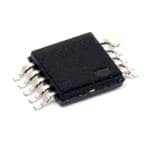
ICGOO电子元器件商城为您提供AD5290YRMZ50由Analog设计生产,在icgoo商城现货销售,并且可以通过原厂、代理商等渠道进行代购。 AD5290YRMZ50价格参考。AnalogAD5290YRMZ50封装/规格:数据采集 - 数字电位器, Digital Potentiometer 50k Ohm 1 Circuit 256 Taps SPI Interface 10-MSOP。您可以下载AD5290YRMZ50参考资料、Datasheet数据手册功能说明书,资料中有AD5290YRMZ50 详细功能的应用电路图电压和使用方法及教程。
AD5290YRMZ50是Analog Devices Inc.推出的一款数字电位器,属于数据采集类器件,具有50 kΩ标称电阻值,采用16引脚MSOP封装。该器件通过I²C接口进行数字控制,可实现精确的电阻调节,适用于需要远程或自动调节电阻值的电子系统。

其主要应用场景包括:
1. 增益与偏置调节:在运算放大器、仪表放大器等模拟电路中,用于动态调节放大倍数或偏置电压,提升系统灵活性。
2. 电源管理:用于调节开关电源或稳压器的反馈网络,实现输出电压的数字编程控制。
3. 传感器校准:在工业传感器、温度测量系统中,用于补偿传感器漂移或非线性误差,提高测量精度。
4. 音频设备:作为音量控制或音调调节元件,替代传统机械电位器,实现更稳定、可靠的数字控制。
5. 便携式仪器:因其小尺寸和低功耗特性,广泛应用于手持测试设备、医疗监测设备等对空间和功耗敏感的场合。

AD5290YRMZ50具备宽电源电压范围(2.7 V至5.5 V)、低温漂和高分辨率(256阶调节),确保在各种环境下的稳定性能。同时支持非易失性存储设置,掉电后仍可保留上次配置,进一步增强了实用性。总体而言,该器件适用于工业控制、通信、消费电子及医疗设备等领域,是实现精密模拟调节的理想选择。
| 参数 | 数值 |
| 产品目录 | 集成电路 (IC)半导体 |
| 描述 | IC DGTL POT 50K 256POS 10MSOP数字电位计 IC IC +/-15V 8-Bit |
| DevelopmentKit | EVAL-AD5290EBZ |
| 产品分类 | |
| 品牌 | Analog Devices |
| 产品手册 | |
| 产品图片 |
|
| rohs | 符合RoHS无铅 / 符合限制有害物质指令(RoHS)规范要求 |
| 产品系列 | 数字电位计 IC,Analog Devices AD5290YRMZ50- |
| 数据手册 | |
| 产品型号 | AD5290YRMZ50 |
| POT数量 | Single |
| 产品目录页面 | |
| 产品种类 | 数字电位计 IC |
| 供应商器件封装 | 10-MSOP |
| 包装 | 管件 |
| 商标 | Analog Devices |
| 存储器类型 | 易失 |
| 安装类型 | 表面贴装 |
| 安装风格 | SMD/SMT |
| 容差 | 30 % |
| 封装 | Tube |
| 封装/外壳 | 10-TFSOP,10-MSOP(0.118",3.00mm 宽) |
| 封装/箱体 | MSOP-10 |
| 工作温度 | -40°C ~ 125°C |
| 工作电源电压 | 5.5 V |
| 工厂包装数量 | 50 |
| 弧刷存储器 | Volatile |
| 抽头 | 256 |
| 接口 | 4 线 SPI(芯片选择) |
| 数字接口 | SPI |
| 最大工作温度 | + 105 C |
| 最小工作温度 | - 40 C |
| 标准包装 | 50 |
| 每POT分接头 | 256 |
| 温度系数 | 35 PPM / C |
| 电压-电源 | 4.5 V ~ 30 V, ±4.5 V ~ 15 V |
| 电源电压-最大 | 30 V |
| 电源电压-最小 | 20 V |
| 电源电流 | 15 uA |
| 电路数 | 1 |
| 电阻 | 50 kOhms |
| 电阻(Ω) | 50k |
| 系列 | AD5290 |
| 配用 | /product-detail/zh/EVAL-AD5290EBZ/EVAL-AD5290EBZ-ND/1858260 |


- 商务部:美国ITC正式对集成电路等产品启动337调查
- 曝三星4nm工艺存在良率问题 高通将骁龙8 Gen1或转产台积电
- 太阳诱电将投资9.5亿元在常州建新厂生产MLCC 预计2023年完工
- 英特尔发布欧洲新工厂建设计划 深化IDM 2.0 战略
- 台积电先进制程称霸业界 有大客户加持明年业绩稳了
- 达到5530亿美元!SIA预计今年全球半导体销售额将创下新高
- 英特尔拟将自动驾驶子公司Mobileye上市 估值或超500亿美元
- 三星加码芯片和SET,合并消费电子和移动部门,撤换高东真等 CEO
- 三星电子宣布重大人事变动 还合并消费电子和移动部门
- 海关总署:前11个月进口集成电路产品价值2.52万亿元 增长14.8%


PDF Datasheet 数据手册内容提取
Compact +30 V / ±15 V 256-Position Digital Potentiometer Data Sheet AD5290 FEATURES FUNCTIONAL BLOCK DIAGRAM 256 position 10 kΩ, 50 kΩ, 100 kΩ AD5290 VDD +20 V to +30 V single-supply operation SDO Q A ±3-1w0i Vre t SoP ±I®1-5c oVm dpuaatl-ibsulep spelyri aolp ienrtaetrifoanc e RSE8EG-RIBSIIATTELR 8 L8A-TBCITH 8 W Low temperature coefficient 35 ppm/°C typical THD 0.006% typical SDI D CK Midscale preset B RS Compact MSOP-10 package CLK Automotive temperature range: −40°C to +125°C CS POR VSS iCMOS™1 process technology A PPLICATIONS DGND 04716-001 Figure 1. High voltage DAC Programmable power supply Programmable gain and offset adjustment Programmable filters and delays Actuator control Audio volume control Mechanical potentiometer replacement GENERAL DESCRIPTION The AD5290 is one of the few high voltage, high performance, With digital rather than manual control, the AD5290 provides and compact digital potentiometers2, 3 in the market at present. layout flexibility and allows closed-loop dynamic controllability. This device can be used as a programmable resistor or resistor The AD5290 is available in MSOP-10 package and has 10 kΩ, divider. The AD5290 performs the same electronic adjustment 50 kΩ, and 100 kΩ options. All parts are guaranteed to operate function as mechanical potentiometers, variable resistors, and over the −40°C to +125°C extended automotive temperature range. trimmers, with enhanced resolution, solid-state reliability, and superior temperature stability. 1 iCMOS™ Process Technology. For analog systems designers who need high performance ICs at higher voltage levels, iCMOS is a technology platform that enables the development of analog ICs capable of 30 V and operating at ±15 V supplies while allowing dramatic reductions in power consumption and package size, and increased ac and dc performance. 2 The terms digital potentiometer and RDAC are used interchangeably. 3 The RDAC segmentation is protected by U.S. Patent Number 5,495,245. Rev. C Information furnished by Analog Devices is believed to be accurate and reliable. However, no responsibility is assumed by Analog Devices for its use, nor for any infringements of patents or other One Technology Way, P.O. Box 9106, Norwood, MA 02062-9106, U.S.A. rights of third parties that may result from its use. Specifications subject to change without notice. No license is granted by implication or otherwise under any patent or patent rights of Analog Devices. Tel: 781.329.4700 www.analog.com Trademarks and registered trademarks are the property of their respective owners. Fax: 781.461.3113 ©2005-2011 Analog Devices, Inc. All rights reserved.
AD5290 Data Sheet TABLE OF CONTENTS Features .............................................................................................. 1 Programming the Variable Resistor ......................................... 15 Applications ....................................................................................... 1 Programming the Potentiometer Divider ............................... 16 Functional Block Diagram .............................................................. 1 3-Wire Serial Bus Digital Interface .......................................... 16 General Description ......................................................................... 1 Daisy Chain Operation .............................................................. 16 Revision History ............................................................................... 2 ESD Protection ........................................................................... 17 Specifications ..................................................................................... 3 Terminal Voltage Operating Range ......................................... 17 Electrical Characteristics—10 kΩ Version ................................ 3 Power-Up and Power-Down Sequences .................................. 17 Electrical Characteristics—50 kΩ, 100 kΩ Versions ............... 5 Layout and Power Supply Biasing ............................................ 17 Interface Timing Characteristics ................................................ 7 Applications ..................................................................................... 18 3-Wire Digital Interface ................................................................... 8 High Voltage DAC ...................................................................... 18 Absolute Maximum Ratings ............................................................ 9 Programmable Power Supply ................................................... 18 ESD Caution .................................................................................. 9 Audio Volume Control .............................................................. 18 Pin Configuration and Descriptions ............................................ 10 Outline Dimensions ....................................................................... 20 Typical Performance Characteristics ........................................... 11 Ordering Guide .......................................................................... 20 Theory of Operation ...................................................................... 15 REVISION HISTORY 11/11—Rev. B to Rev. C 7/09—Rev. 0 to Rev. A Change to Figure 33 ....................................................................... 18 Changes to Features Section ............................................................ 1 4/10—Rev. A to Rev. B Changes to Ordering Guide .......................................................... 20 Changes to Figure 29 ...................................................................... 16 12/05—Revision 0: Initial Version Updated Outline Dimensions ....................................................... 20 Rev. C | Page 2 of 20
Data Sheet AD5290 SPECIFICATIONS ELECTRICAL CHARACTERISTICS—10 kΩ VERSION V /V = ±15 V ± 10%, V = V , V = V or 0 V, −40°C < T < +125°C, unless otherwise noted. DD SS A DD B SS A Table 1. Parameter Symbol Conditions Min Typ1 Max Unit DC CHARACTERISTICS RHEOSTAT MODE Resistor Differential NL2 R-DNL R , V = NC −1 ±0.3 +1 LSB WB A Resistor Nonlinearity2 R-INL R , V = NC −1.5 ±0.7 +1.5 LSB WB A Nominal Resistor Tolerance ∆R T = +25°C −30 +30 % AB A Resistance Temperature Coefficient3 (∆R /R )/∆T×106 V = V , wiper = no connect 35 ppm/°C AB AB AB DD Wiper Resistance R 50 100 Ω W DC CHARACTERISTICS POTENTIOMETER DIVIDER MODE Integral Nonlinearity4 INL −1 ±0.3 +1 LSB Differential Nonlinearity4 DNL −1 ±0.3 +1 LSB Voltage Divider Temperature Coefficient (∆V /V )/∆T×106 Code = 0x80 5 ppm/°C W W Full-Scale Error V Code = 0xFF −6 −4 0 LSB WFSE Zero-Scale Error V Code = 0x00 0 +3 +5 LSB WZSE RESISTOR TERMINALS Voltage Range5 V V V V A, B, W SS DD Capacitance6 A, B C f = 1 MHz, measured to GND, 45 pF A, B code = 0x80 Capacitance6 C f = 1 MHz, measured to GND, 60 pF W code = 0x80 Common-Mode Leakage I V = V = V 1 nA CM A B W DIGITAL INPUTS AND OUTPUTS Input Logic High (CS, CLK, SDI) VIH 2.4 V Input Logic Low (CS, CLK, SDI) VIL 0.8 V Output Logic High (SDO) V R = 2.2 kΩ to 5 V 4.9 V OH Pull-up Output Logic Low (SDO) V I = 1.6 mA 0.4 V OL OL Input Current I V = 0 V or 5 V ±1 µA IL IN Input Capacitance6 C 5 pF IL POWER SUPPLIES Positive Supply Current I V = +5 V or V = 0 V, 15 50 μA DD IH IL V /V = ±15 V DD SS Negative Supply Current I V = +5 V or V = 0 V, −0.01 −1 μA SS IH IL V /V = ±15 V DD SS Power Dissipation7 P V = +5 V or V = 0 V, 765 μW DISS IH IL V /V = ±15 V DD SS Power Supply Rejection Ratio PSRR ΔV /ΔV = ±15 V ± 10% −0.15 ±0.08 +0.15 %/% DD SS Rev. C | Page 3 of 20
AD5290 Data Sheet Parameter Symbol Conditions Min Typ1 Max Unit DYNAMIC CHARACTERISTICS6, 8, 9 Bandwidth −3 dB BW Code = 0x80 470 kHz Total Harmonic Distortion THD V = 1 V rms, V = 0 V, f = 1 kHz 0.006 % W A B V Settling Time t V = 10 V, V = 0 V, ±1 LSB error 4 µs W S A B band Resistor Noise Voltage e R = 5 kΩ, f = 1 kHz 9 nV/√Hz N_WB WB 1 Typical represents average reading at +25°C, VDD = +15 V, and VSS = −15 V. 2 Resistor position nonlinearity error R-INL is the deviation from an ideal value measured between the maximum resistance and the minimum resistance wiper positions. R-DNL measures the relative step change from an ideal value measured between successive tap positions. Parts are guaranteed monotonic. 3 All parts have a 35 ppm/°C temperature coefficient. 4 INL and DNL are measured at VW with the RDAC configured as a potentiometer divider similar to a voltage output DAC. VA = VDD and VB = 0 V. DNL specification limits of ±1 LSB maximum are guaranteed monotonic operating conditions. 5 Resistor Terminal A, Terminal B, and Terminal W have no limitations on polarity with respect to each other. 6 Guaranteed by design and not subject to production test. 7 PDISS is calculated from (IDD × VDD) + abs (ISS × VSS). CMOS logic-level inputs result in minimum power dissipation. 8 Bandwidth, noise, and settling times are dependent on the terminal resistance value chosen. The lowest R value results in the fastest settling time and highest bandwidth. The highest R value results in the minimum overall power consumption. 9 All dynamic characteristics use VDD = +15 V and VSS = −15 V. Rev. C | Page 4 of 20
Data Sheet AD5290 ELECTRICAL CHARACTERISTICS—50 KΩ, 100 KΩ VERSIONS V /V = ±15 V ± 10%, V = +V , V = V or 0 V, −40°C < T < +125°C, unless otherwise noted. DD SS A DD B SS A Table 2. Parameter Symbol Conditions Min Typ1 Max Unit DC CHARACTERISTICS RHEOSTAT MODE Resistor Differential NL2 R-DNL R , V = NC −0.5 ±0.1 +0.5 LSB WB A Resistor Nonlinearity2 R-INL R , V = NC −1 ±0.5 +1 LSB WB A Nominal Resistor Tolerance ∆R T = +25°C −30 +30 % AB A Resistance Temperature Coefficient3 (∆R /R )/∆T×106 V = V , wiper = no connect 35 ppm/°C AB AB AB DD Wiper Resistance R 50 100 Ω W DC CHARACTERISTICS POTENTIOMETER DIVIDER MODE Integral Nonlinearity4 INL −1 ±0.5 +1 LSB Differential Nonlinearity4 DNL −1 ±0.5 +1 LSB Voltage Divider Temperature (∆V /V )/∆T×106 Code = 0x80 5 ppm/°C W W Coefficient Full-Scale Error V Code = 0xFF −2.5 −1.6 0 LSB WFSE Zero-Scale Error V Code = 0x00 0 +0.6 +1.5 LSB WZSE RESISTOR TERMINALS Voltage Range5 V V V V A, B, W SS DD Capacitance6 A, B C f = 1 MHz, measured to GND, 45 pF A, B code = 0x80 Capacitance6 C f = 1 MHz, measured to GND, 60 pF W code = 0x80 Common-Mode Leakage I V = V = V 1 nA CM A B W DIGITAL INPUTS AND OUTPUTS Input Logic High (CS, CLK, SDI) V 2.4 V IH Input Logic Low (CS, CLK, SDI) V 0.8 V IL Output Logic High (SDO) V R = 2.2 kΩ to 5 V 4.9 V OH Pull-up Output Logic Low (SDO) V I = 1.6 mA 0.4 V OL OL Input Current I V = 0 V or 5 V ±1 µA IL IN Input Capacitance6 C 5 pF IL POWER SUPPLIES Positive Supply Current I V = +5 V or V = 0 V, 15 50 μA DD IH IL V /V = ±15 V DD SS Negative Supply Current I V = +5 V or V = 0 V, −0.01 −1 μA SS IH IL V /V = ±15 V DD SS Power Dissipation7 P V = +5 V or V = 0 V, 765 μW DISS IH IL V /V = ±15 V DD SS Power Supply Rejection Ratio PSRR ΔV /ΔV = ±15 V ± 10% −0.05 ±0.01 +0.05 %/% DD SS Rev. C | Page 5 of 20
AD5290 Data Sheet Parameter Symbol Conditions Min Typ1 Max Unit DYNAMIC CHARACTERISTICS6, 8, 9 Bandwidth −3 dB BW R = 50 kΩ, code = 0x80 90 kHz AB R = 100 kΩ, code = 0x80 50 kHz AB Total Harmonic Distortion THD V = 1 V rms, V = 0 V, f = 1 kHz 0.002 % W A B V Settling Time t V = 10 V, V = 0 V, 4 µs W S A B ±1 LSB error band Resistor Noise Voltage e R = 25 kΩ, f = 1 kHz 20 nV√Hz N_WB WB 1 Typical represents average reading at +25°C, VDD = +15 V, and VSS = −15 V. 2 Resistor position nonlinearity error R-INL is the deviation from an ideal value measured between the maximum resistance and the minimum resistance wiper positions. R-DNL measures the relative step change from an ideal value measured between successive tap positions. Parts are guaranteed monotonic. 3 All parts have a 35 ppm/°C temperature coefficient. 4 INL and DNL are measured at VW with the RDAC configured as a potentiometer divider similar to a voltage output DAC. VA = VDD and VB = 0 V. DNL specification limits of ±1 LSB maximum are guaranteed monotonic operating conditions. 5 Resistor Terminal A, Terminal B, and Terminal W have no limitations on polarity with respect to each other. 6 Guaranteed by design and not subject to production test. 7 PDISS is calculated from (IDD × VDD) + abs (ISS × VSS). CMOS logic level inputs result in minimum power dissipation. 8 Bandwidth, noise, and settling times are dependent on the terminal resistance value chosen. The lowest R value results in the fastest settling time and highest bandwidth. The highest R value results in the minimum overall power consumption. 9 All dynamic characteristics use VDD = +15 V and VSS = −15 V. Rev. C | Page 6 of 20
Data Sheet AD5290 INTERFACE TIMING CHARACTERISTICS Table 3. Parameter 1, 2 Symbol Conditions Min Typ Max Unit Clock Frequency f 4 MHz CLK Input Clock Pulse Width t , t Clock level high or low 120 ns CH CL Data Setup Time t 30 ns DS Data Hold Time t 20 ns DH CLK to SDO Propagation Delay3 t R = 2.2 kΩ, C < 20 pF 10 100 ns PD Pull-up L CS Setup Time t 120 ns CSS CS High Pulse Width t 150 ns CSW CLK Fall to CS Fall Hold Time t 10 ns CSH0 CLK Rise to CS Rise Hold Time t 120 ns CSH CS Rise to Clock Rise Setup t 120 ns CS1 1 See Figure 3 for the location of the measured values. All input control voltages are specified with tR = tF = 1 ns (10% to 90% of VDD) and timed from a voltage level of 1.6 V. Switching characteristics are measured using VDD = +15 V and VSS = −15 V. 2 Guaranteed by design and not subject to production test. 3 Propagation delay depends on the value of VDD, RPull-up, and CL. Rev. C | Page 7 of 20
AD5290 Data Sheet 3-WIRE DIGITAL INTERFACE Data is loaded MSB first. (DATAS IND)I 1 DX DX 0 Table 4. AD5290 Serial Data-Word Format tDS B7 B6 B5 B4 B3 B2 B1 B0 tDH 1 D7 D6 D5 D4 D3 D2 D1 D0 (DATA OSUDTO) D'X D'X 0 MSB LSB tPD_MAX 27 20 tCH 1 CLK tCS1 0 tCSH0 tCL 1 SDI 0 D7 D6 D5 D4 D3 D2 D1 D0 1 tCSS tCSH 1 CS tCSW CLK 0 0 tS 1 CS RDAC REGISTER LOAD VDD VOUT 010 04716-002 VOUT 0V ±1 LSB ERROR BAND ±1 LSB 04716-003 Figure 2. AD5290 3-Wire Digital Interface Timing Diagram Figure 3. Detail Timing Diagram (VA = VDD, VB = 0 V, VW = VOUT) Rev. C | Page 8 of 20
Data Sheet AD5290 ABSOLUTE MAXIMUM RATINGS T = +25°C, unless otherwise noted. Stresses above those listed under Absolute Maximum Ratings A may cause permanent damage to the device. This is a stress Table 5. rating only; functional operation of the device at these or any Parameter Rating other conditions above those indicated in the operational V to GND −0.3 V, +35 V DD section of this specification is not implied. Exposure to absolute V to GND +0.3 V, −16.5 V SS maximum rating conditions for extended periods may affect V to V −0.3 V, +35 V DD SS device reliability. V , V , V to GND V , V A B W SS DD Maximum Current ESD CAUTION I , I Pulsed ±20 mA WB WA I Continuous (R ≤ 6 kΩ, A Open, ±5 mA WB WB V /V = 30 V/0 V)1 DD SS I Continuous (R ≤ 6 kΩ, B Open, ±5 mA WA WA VDD/VSS = 30 V/0 V)1 Digital Input and Output Voltages to GND 0 V, +7 V Operating Temperature Range −40°C to +125°C Maximum Junction Temperature (T )2 +150°C JMAX Storage Temperature −65°C to +150°C Lead Temperature 245°C (Soldering, 10 sec to 30 sec) Thermal Resistance2 θ : MSOP-10 230°C/W JA 1 The maximum terminal current is bound by the maximum current handling of the switches, maximum power dissipation of the package, and the maximum applied voltage across any two of the following at a given resistance: A terminal, B terminal, and W terminal. 2 Package power dissipation = (TJMAX – TA)/θJA. Rev. C | Page 9 of 20
AD5290 Data Sheet PIN CONFIGURATION AND DESCRIPTIONS A 1 10 W B 2 AD5290 9 VDD VSS 3 TOP VIEW 8 SDO GNCDS 45 (Not to Scale) 76 SCDLKI 04716-004 Figure 4. AD5290 Pin Configuration Table 6. AD5290 Pin Function Descriptions Pin No. Mnemonic Description 1 A A Terminal. V ≤ V ≤ V . SS A DD 2 B B Terminal. V ≤ V ≤ V . SS B DD 3 V Negative Supply. Connect to 0 V for single-supply applications. SS 4 GND Digital Ground. 5 CS Chip Select Input; Active Low. When CS returns high, data is loaded into the wiper register. 6 CLK Serial Clock Input. Positive edge triggered. 7 SDI Serial Data Input Pin. Shifts in one bit at a time on positive clock CLK edges. MSB loaded first. 8 SDO Serial Data Output Pin. Internal N-Ch FET with open-drain output that requires external pull-up resistor. It shifts out the previous eight SDI bits that allow daisy-chain operation of multiple packages. 9 V Positive Power Supply. DD 10 W W Terminal. V ≤ V ≤ V . SS W DD Rev. C | Page 10 of 20
Data Sheet AD5290 TYPICAL PERFORMANCE CHARACTERISTICS 1.0 1.0 VDD = 16.5V VDD = 16.5V 0.8 0.8 –40°C B) –40°C 0.6 +25°C S 0.6 +25°C SB) +125°C L (L +125°C L 0.4 N 0.4 NL ( E D E I 0.2 OD 0.2 D M T MO 0 TER 0 A –0.2 E –0.2 T M RHEOS ––00..46 OTENTIO ––00..46 P ––01..80 04716-029 ––01..80 04716-032 0 32 64 96 128 160 192 224 256 0 32 64 96 128 160 192 224 256 CODE (Decimal) CODE (Decimal) Figure 5. Resistance Step Position Nonlinearity Error vs. Code Figure 8. Potentiometer Divider Differential Nonlinearity Error vs. Code 1.0 20 VDD = 16.5V 0.8 –40°C 16 IDD @ VDD/VSS = 30V/0V NL (LSB) 00..64 ++2152°5C°C µT (A) 12 IDD @ VDD/VSS =±15V MODE D 0.20 CURREN 8 AT –0.2 LY T P EOS –0.4 SUP 4 ISS @ VDD/VSS = 30V/0V H R –0.6 0 ––01..80 04716-030 –4 ISS @ VDD/VSS =±15V 04716-005 0 32 64 96 128 160 192 224 256 –40 –20 0 20 40 60 80 100 120 CODE (Decimal) TEMPERATURE (°C) Figure 6. Resistance Step Change Differential Nonlinearity Error vs. Code Figure 9. Supply Current IDD vs. Temperature 1.0 VDD = 16.5V 120 VDD/VSS =±15V 0.8 100kΩ MODE INL (LSB) 000...642 –++421052°°5CC°C ΩANCE, R (k)AB 10800 TER 0 SIST 60 50kΩ ME –0.2 RE NTIO –0.4 TAL 40 E O T T O –0.6 P ––01..80 04716-031 200–40 –20 0 20 1400kΩ 60 80 100 120 04716-007 0 32 64 96 128 160 192 224 256 CODE (Decimal) TEMPERATURE (°C) Figure 7. Potentiometer Divider Nonlinearity Error vs. Code Figure 10. Total Resistance vs. Temperature Rev. C | Page 11 of 20
AD5290 Data Sheet 100 0 0x80 80 –6 °m/C) 60 1500kk –12 0x40 O (pp 40 100k –18 0x20 C 0x10 MP 20 –24 DE TE 0 (dB) –30 00xx0084 O M –20 –36 T 0x02 TA –40 –42 0x01 S O E –60 –48 H R ––18000 04716-033 ––5640 04716-023 0 32 64 96 128 160 192 224 256 1k 10k 100k 1M CODE (Decimal) (Hz) Figure 11. (ΔRWB/RWB)/ΔT Rheostat Mode Tempco Figure 14. 50 kΩ Gain vs. Frequency vs. Code 100 0 °m/C) 80 10k –6 00xx8400 pp 60 50k –12 O ( 100k 0x20 C 40 –18 P M 0x10 TE 20 –24 ODE 0 dB) –30 0x08 ER M –20 ( –36 0x04 T 0x02 E M –40 –42 O 0x01 NTI –60 –48 E POT ––18000 04716-034 ––5640 04716-024 0 32 64 96 128 160 192 224 256 1k 10k 100k 1M CODE (Decimal) (Hz) Figure 12. (ΔVWB/VWB)/ΔT Potentiometer Mode Tempco Figure 15. 100 kΩ Gain vs. Frequency vs. Code 0 0x80 –6 0x40 –12 0x20 –18 0x10 –24 0x08 dB) –30 0x04 ( –36 0x02 –42 0x01 –48 ––5640 04716-022 04716-035 1k 10k 100k 1M (Hz) Figure 13. 10 kΩ Gain vs. Frequency vs. Code Figure 16. Midscale Transition Glitch Rev. C | Page 12 of 20
Data Sheet AD5290 –60 6 CODE = 80H, VDD/VSS =±15V, VA/VB =±10V VDD/VSS = 30V/0V B) VA = VDD O (d 5 VB = 0V TI A) A m ON R –40 (MAX 4 RAB = 10kΩ ER SUPPLY REJECTI –20 +PSRR– P@S RVRDD @/V VSSD D=/V±1S5SV = D±C15±V 1D0C%± p 1-p0 %A Cp-p AC THEORETICAL IWB_ 32 RAB = 50kΩ W 1 PO 0 04716-036 0 RAB = 100kΩ 04716-027 100 1k 10k 100k 1M 0 64 128 192 256 FREQUENCY (Hz) CODE (Decimal) Figure 17. Power Supply Rejection vs. Frequency Figure 20. Theoretical Maximum Current vs. Code 1 140 VCDODD/VES =S M=I±D1S5CVALE VDD = +15V VIN = 1VRMS 120 VVSDSIG = =– +155VV A) 0.01 10kΩ µ (D 100 D %) T I N ( 100kΩ EN 80 CODE = AA D + URR H C 60 T 0.001 50kΩ PLY UP 40 S CODE = FF 0.0001 04716-009 200 04716-037 10 100 1k 10k 100k 10k 100k 1M 10M FREQUENCY (Hz) FREQUENCY (Hz) Figure 18. Total Harmonic Distortion Plus Noise vs. Frequency Figure 21. Supply Current IDD vs. Frequency 1 10 VDD/VSS =±15V VDD = +15V CODE = MIDSCALE VSS =–15V fIN = 1kHz VDIG = +5V 8 A) n 0.1 (SS D + N (%) URRENT I 6 CODE = AA TH 50kΩ Y C 4 L 0.01 10kΩ PP U S CODE = FF 2 100kΩ 0.001 04716-010 0 04716-038 0.001 0.01 0.1 1 10 10k 100k 1M 10M AMPLITUDE (V) FREQUENCY (Hz) Figure 19. Total Harmonic Distortion Plus Noise vs. Amplitude Figure 22. Supply Current ISS vs. Frequency Rev. C | Page 13 of 20
AD5290 Data Sheet 1000 A) µ (D D T I N E RR 100 U C Y L P UP VDD/VSS =±16.5V S 100 1 2 3 4 5 04716-039 04716-041 DIGITAL INPUT VOLTAGE VIH (V) Figure 23. Supply Current vs. Digital Input Voltage Figure 25. Large Signal Settling Time, Code = 0x00 to 0xFF 04716-040 Figure 24. Digital Feedthrough Rev. C | Page 14 of 20
Data Sheet AD5290 THEORY OF OPERATION PROGRAMMING THE VARIABLE RESISTOR where: Rheostat Operation D is the decimal equivalent of the binary code loaded in the 8-bit RDAC register from 0 to 255. The part operates in the rheostat mode when only two termi- R is the end-to-end resistance. nals are used as a variable resistor. The unused terminal can AB R is one of the wiper resistances contributed by the on be floating or tied to the W terminal as shown in Figure 26. W resistance of an internal switch. A A A The AD5290 wiper switch is designed with the transmission W W W gate CMOS topology and with the gate voltage derived from B B B 04716-011 VteDmDp. Terhaetu wreip. eCro rnetsriastrayn tcoe ,t hReW t,e mis pa efruantuctrieo cno oeff fVicDieDn atn odf the RAB, Figure 26. Rheostat Mode Configuration which is only 35 ppm/°C, the temperature coefficient of the wiper resistance is significantly higher because the wiper resistance The nominal resistance between Terminal A and Terminal B, doubles from 25°C to 125°C. As a result, the user must take into RAB, is available in 10 kΩ, 50 kΩ, and 100 kΩ with ±30% toler- consideration the contribution of RW on the desirable ance and has 256 tap points accessed by the wiper terminal. The resistance. On the other hand, the wiper resistance is insensitive 8-bit data in the RDAC latch is decoded to select one of the 256 to the tap point potential. As a result, RW remains relatively flat possible settings. Figure 27 shows a simplified RDAC structure. at a given V and temperature at various codes. DD A Assuming that an ideal 10 kΩ part is used, the wiper’s first 4RS connection starts at the B terminal for the programming code of 0x00 where SWB is closed. The minimum resistance between 4RS Terminal W and Terminal B is, therefore, generally 150 Ω. The second connection is the first tap point, which corresponds to 4RS 2RS 189 Ω (RWB = 1/256 × RAB + 3RW = 39 Ω + 150 Ω) for code 0x01, and so on. Each LSB data value increase moves the wiper up the 2RS RW resistor ladder until the last tap point is reached at 10,110 Ω. RS In the zero-scale condition, a finite total wiper resistance of W 150 Ω is present. Regardless of which setting the part is oper- RW RS ating in, care should be taken to limit the current between 8-BIT ADDRESS DECODER 2RS the A terminal to B terminal, W terminal to A terminal, and RW W terminal to B terminal, to the maximum dc current of 5 mA or pulse current of 20 mA. Otherwise, degradation, or possible 4RS 2RS destruction of the internal switch contact, can occur. 4RS Similar to the mechanical potentiometer, the resistance of the RDAC between the W terminal and the A terminal also B produces a digitally controlled complementary resistance, R . WA 04716-012 RthWeA d satatar tlso aatd tehde i mntaox tihmeu lmatc rhe sinisctarenacsee sv.a Tluhee a gnedn edreaclr eeqasueast iaosn Figure 27. AD5290 Simplified RDAC Circuit. for this operation is (RS = Step Resistor, RW = Wiper Resistor) 256−D R (D)= ×R +3×R (2) In order to achieve optimum cost performance, Analog Devices WA 256 AB W has patented the RDAC segmentation architecture for all the digital potentiometers. In particular, the AD5290 employs a 3-stage segmentation approach as shown in Figure 27. As a result, the general equation determining the digitally programmed output resistance between the W terminal and B terminal is D R (D)= ×R +3×R (1) WB 256 AB W Rev. C | Page 15 of 20
AD5290 Data Sheet PROGRAMMING THE POTENTIOMETER DIVIDER 3-WIRE SERIAL BUS DIGITAL INTERFACE Voltage Output Operation The AD5290 contains a 3-wire digital interface (CS, CLK, The digital potentiometer easily generates a voltage divider and SDI). The 8-bit serial word must be loaded MSB first. at wiper to B and wiper to A proportional to the input voltage The format of the word is shown in Table 4. The positive edge at A to B. Unlike the polarity of V to GND, which must be sensitive CLK input requires clean transitions to avoid clocking DD positive, voltage across A to B, W to A, and W to B can be at incorrect data into the serial input register. Standard logic fami- either polarity. lies work well. When CS is low, the clock loads data into the serial register on each positive clock edge. VI A The data setup and data hold times in the Specifications section W VO determine the valid timing requirements. The AD5290 uses an 8-bit serial input data register word that is transferred to the B 04716-013 internal RDAC register when the CS line returns to logic high. Extra MSB bits are ignored. Figure 28. Potentiometer Mode Configuration DAISY CHAIN OPERATION If ignoring the effect of the wiper resistance for simplicity, con- necting the A terminal to 30 V and the B terminal to ground SDO shifts out the SDI content in the previous frame; thus it produces an output voltage at the Wiper W to Terminal B can be used for daisy-chaining multiple devices. The SDO pin ranging from 0 V to 1 LSB less than 30 V. Each LSB of voltage contains an open drain N-Ch MOSFET and requires a pull- is equal to the voltage applied across Terminal A and Terminal B, up resistor if the SDO function is used. Users need to tie the divided by the 256 positions of the potentiometer divider. The SDO pin of one package to the SDI pin of the next package. general equation defining the output voltage at V with respect Users may need to increase the clock period because the pull-up W to ground for any valid input voltage applied to Terminal A and resistor and the capacitive loading at the SDO to SDI interface Terminal B is can induce time delay to the subsequent devices. D 256−D V (D)= ×V + ×V (3) For example, in Figure 29, if two AD5290s are daisy-chained, a W 256 A 256 B total of 16 bits of data are required for each operation. The first set of eight bits goes to U2, and the second set of eight bits goes Operation of the digital potentiometer in the divider mode to U1. The CS should be kept low until all 16 bits are clocked results in a more accurate operation over temperature. Unlike into their respective serial registers. The CS is then pulled high the rheostat mode, the output voltage is dependent mainly on the ratio of the internal resistors R and R and not the to complete the operation. WA WB absolute values. Therefore, the temperature drift reduces to +5V 5 ppm/°C. AD5290 AD5290 U1 R2.P2UkΩ U2 µC MOSI SDI SDO SDI SDO SCLK SS CS CLK CS CLK 04716-014 Figure 29. Daisy Chain Configuration Rev. C | Page 16 of 20
Data Sheet AD5290 ESD PROTECTION POWER-UP AND POWER-DOWN SEQUENCES All digital inputs are protected with a series input resistor and Because of the ESD protection diodes that limit the voltage a Zener ESD structure, as shown in Figure 30. These structures compliance at Terminal A, Terminal B, and Terminal W apply to digital input pins, Pin CS, Pin CLK, Pin SDI, and (Figure 31), it is important to power VDD/VSS before applying Pin SDO. any voltage to Terminal A, Terminal B, and Terminal W. Otherwise, the diodes are forward-biased such that V /V DD SS 340Ω LOGIC are powered unintentionally and affect the system. Similarly, GND 04716-015 VseDqDu/eVnScS es hiso ausl dfo blelo pwosw: GerNedD d, oVwDDn, lVasSSt,. dTihgeit aidl einalp puotsw, earn-du p V /V /V . The order of powering V , V , V , and the digital Figure 30. Equivalent ESD Protection Circuit A B W A B W inputs is not important, as long as they are powered after All analog terminals are also protected by Zener ESD protection VDD/VSS. diodes, as shown in Figure 31. LAYOUT AND POWER SUPPLY BIASING VDD It is good practice to use a compact, minimum lead-length layout design. The leads to the input should be as direct as A possible, with a minimum conductor length. Ground paths should have low resistance and low inductance. W B Similarly, it is also good practice to bypass the power supplies with quality capacitors. Low equivalent series resistance (ESR), VSS 04716-016 1ap µpFli etod 1a0t tµhFe tsaunptpalluiems t oor m eliencitmroizlyet iacn cya tpraacnistioernst, sdhisotuulrdb abnec e Figure 31. Equivalent ESD Protection Analog Pins and to filter low frequency ripple. Figure 32 illustrates the basic supply-bypassing configuration for the AD5290. TERMINAL VOLTAGE OPERATING RANGE The AD5290 V and V power supplies define the boundary The ground pin of the AD5290 is a digital ground reference. DD SS conditions for proper 3-terminal digital potentiometer opera- To minimize the digital ground bounce, the AD5290 digital tion. The AD5290 can operate in single supply from +4.5 V to ground terminal should be joined remotely to the analog +33 V or dual supply from ±4.5 V to ±16.5 V. The AD5290 is ground (Figure 32). functional at low supply voltages such as 4.5 V, but the performance parameters are not guaranteed. VDDC3 + C1 VDD 10µF 0.1µF The voltages present on Terminal A, Terminal B, and Terminal W AD5290 that are more positive than VDD or more negative than VSS are C4 + C2 clamped by the internal forward-biased diodes (Figure 31). VSS 10µF 0.1µF VSS GND 04716-017 Figure 32. Power Supply Bypassing Rev. C | Page 17 of 20
AD5290 Data Sheet APPLICATIONS HIGH VOLTAGE DAC AUDIO VOLUME CONTROL AD5290 can be configured as a high voltage DAC, with out- Because of its good THD performance and high voltage put voltage as high as 30 V. The circuit is shown in Figure 33. capability, AD5290 can be used as a digital volume control. The output is If AD5290 is used directly as an audio attenuator or gain amplifier, a large step change in the volume level at any arbi- D R VO(D)256[1.2V (1 R2)] (4) trary time can lead to an abrupt discontinuity of the audio 1 signal causing an audible zipper noise. To prevent this, a zero- where D is the decimal code from 0 to 255. crossing window detector can be inserted to the CS line to delay the device update until the audio signal crosses the VDD window. Since the input signal can operate on top of any RBIAS VDD dc level rather than absolute zero volt level, zero-crossing in this case means the signal is ac-coupled, and the dc offset U1A U2 level is the signal zero reference point. V+ AD5290 D1 OP284 ADR512 V– 100kΩ U1B The configuration to reduce zipper noise (Figure 35) and the results of using this configuration are shown in Figure 36. The B OP284 VOUT input is ac-coupled by C1 and attenuated down before feeding into the window comparator formed by U2, U3, and U4B R2 R1 (Figure 35). U6 is used to establish the signal zero reference. 04716-018 Tthheer eufpopree,r t lhime oitu otpf utht ep cuolsmesp harigatho wr ihse sneet vaebro tvhee iitns pouffts featl lasn d, Figure 33. High Voltage DAC between 2.502 V and 2.497 V (or 0.005 V window) in this PROGRAMMABLE POWER SUPPLY example. This output is AND’ed with the chip select signal such that the AD5290 updates whenever the signal crosses With a boost regulator, such as ADP1611, AD5290 can be used the window. To avoid a constant update of the device, the as the variable resistor at the regulator’s FB pin to provide the chip select signal should be programmed as two pulses, rather programmable power supply (Figure 34). The output is than as one shown in Figure 36. (D )R V 1.23V [1 256 AB] (5) O R In Figure 35, the lower trace shows that the volume level changes 2 from a quarter-scale to full-scale when a signal change occurs AD5290’s V is derived from the output. Initially, L1 acts as near the zero-crossing window. DD a short, and V is one diode voltage drop below +5 V. The DD output slowly establishes the final value. U1 5V AD5290 C1 VDD A 10CIFN U2 IN L1 0.1F R1 W ADP1611 4.7H 100k B RT SW VOUT 1.23V FB D1 COUT 10F R2 COMP 8.5k CSS SS RC 22nF GND 220k 1C5C0pF 04716-019 Figure 34. Programmable Power Supply Rev. C | Page 18 of 20
Data Sheet AD5290 VIN C1 1µF 5V U1 100kRΩ1 +5V +15V VDD C3 A AD5290 U2 0.1µF V+ R2 ADCM371 C2 R904kΩ 200Ω V– U4B 0–.115µVF VSS W +15UV5 +5V 4 7408 6 1 U4A 100kΩ V+ VOUT R105kΩ U3 5 2 7408 CS V– V+ 5V ADCM371 CLK CLK B U6 V– SDI SDI –15V AD8V5+41 R3 CS GND 100kΩ V– 04716-028 Figure 35. Audio Volume Control with Zipper Noise Reduction 1 2 CHANNEL 1 F1.R0E3VQ p=- p20.25kHz 04716-021 Figure 36. Input (Trace 1) and Output (Trace 2) of the Circuit in Figure 35 (The Command of Volume Change May Occur at Any Time, but the Level Change Occurs Only Near the Zero-Crossing Window) Rev. C | Page 19 of 20
AD5290 Data Sheet OUTLINE DIMENSIONS 3.10 3.00 2.90 10 6 5.15 3.10 4.90 3.00 4.65 2.90 1 5 PIN1 IDENTIFIER 0.50BSC 0.95 15°MAX 0.85 1.10MAX 0.75 0.70 0.15 0.30 6° 0.23 0.55 CO0P.0L5ANARITY 0.15 0° 0.13 0.40 0.10 COMPLIANTTOJEDECSTANDARDSMO-187-BA 091709-A Figure 37. 10-Lead Mini Small Outline Package [MSOP] (RM-10) Dimensions shown in millimeters ORDERING GUIDE Model1 R (kΩ) Temperature Range Package Description Package Option Branding AB AD5290YRMZ10 10 –40°C to +125°C 10-Lead MSOP RM-10 D4U AD5290YRMZ10-R7 10 –40°C to +125°C 10-Lead MSOP RM-10 D4U AD5290YRMZ50 50 –40°C to +125°C 10-Lead MSOP RM-10 D4T AD5290YRMZ50-R7 50 –40°C to +125°C 10-Lead MSOP RM-10 D4T AD5290YRMZ100 100 –40°C to +125°C 10-Lead MSOP RM-10 D4V AD5290YRMZ100-R7 100 –40°C to +125°C 10-Lead MSOP RM-10 D4V EVAL-AD5290EBZ 10 Evaluation Board 1 Z = RoHS Compliant Part. ©2005-2011 Analog Devices, Inc. All rights reserved. Trademarks and registered trademarks are the property of their respective owners. D04716-0-11/11(C) Rev. C | Page 20 of 20
Mouser Electronics Authorized Distributor Click to View Pricing, Inventory, Delivery & Lifecycle Information: A nalog Devices Inc.: EVAL-AD5290EBZ AD5290YRMZ10 AD5290YRMZ50 AD5290YRMZ100 AD5290YRMZ100-R7 AD5290YRMZ10- R7 AD5290YRMZ50-R7