ICGOO在线商城 > 集成电路(IC) > 数据采集 - 数字电位器 > AD5260BRUZ20-RL7

 Datasheet下载
- 型号: AD5260BRUZ20-RL7
- 制造商: Analog
- 库位|库存: xxxx|xxxx
- 要求:
| 数量阶梯 | 香港交货 | 国内含税 |
| +xxxx | $xxxx | ¥xxxx |
查看当月历史价格
查看今年历史价格
AD5260BRUZ20-RL7产品简介:
ICGOO电子元器件商城为您提供AD5260BRUZ20-RL7由Analog设计生产,在icgoo商城现货销售,并且可以通过原厂、代理商等渠道进行代购。 AD5260BRUZ20-RL7价格参考¥23.73-¥36.28。AnalogAD5260BRUZ20-RL7封装/规格:数据采集 - 数字电位器, Digital Potentiometer 20k Ohm 1 Circuit 256 Taps SPI Interface 14-TSSOP。您可以下载AD5260BRUZ20-RL7参考资料、Datasheet数据手册功能说明书,资料中有AD5260BRUZ20-RL7 详细功能的应用电路图电压和使用方法及教程。
AD5260BRUZ20-RL7是Analog Devices Inc.生产的一款数字电位器,属于数据采集类中的数字电位器产品。该器件为128位分辨率的非易失性数字电位器,采用20 kΩ标称电阻值,封装为TSSOP-14,支持SPI串行接口通信。

其主要应用场景包括:

1. 增益调节与信号调理:广泛用于运算放大器、可编程增益放大器(PGA)中,通过数字控制实现精确的增益调节,适用于工业测量、传感器信号调理等需要高精度模拟控制的场合。

2. 电源管理:可用于DC-DC转换器或电压调节电路中,通过调节反馈网络中的电阻值,动态调整输出电压,提高系统灵活性和稳定性。

3. 音频设备:在音频系统中用于音量控制或均衡调节,替代机械电位器,提升可靠性和抗干扰能力。

4. 校准与补偿电路:在精密仪器或自动化测试设备中,用于系统校准,补偿元件老化或温度漂移带来的误差。

5. 便携式设备:由于其低功耗特性和小型封装,适合应用于电池供电的便携式医疗设备、手持仪表等。

AD5260BRUZ20-RL7具备非易失性存储功能,断电后仍能保持最后设置的阻值位置,提升了系统启动的可靠性。同时,其工业级工作温度范围(−40°C至+85°C)使其适用于严苛环境下的工业控制和嵌入式系统。
| 参数 | 数值 |
| 产品目录 | 集成电路 (IC)半导体 |
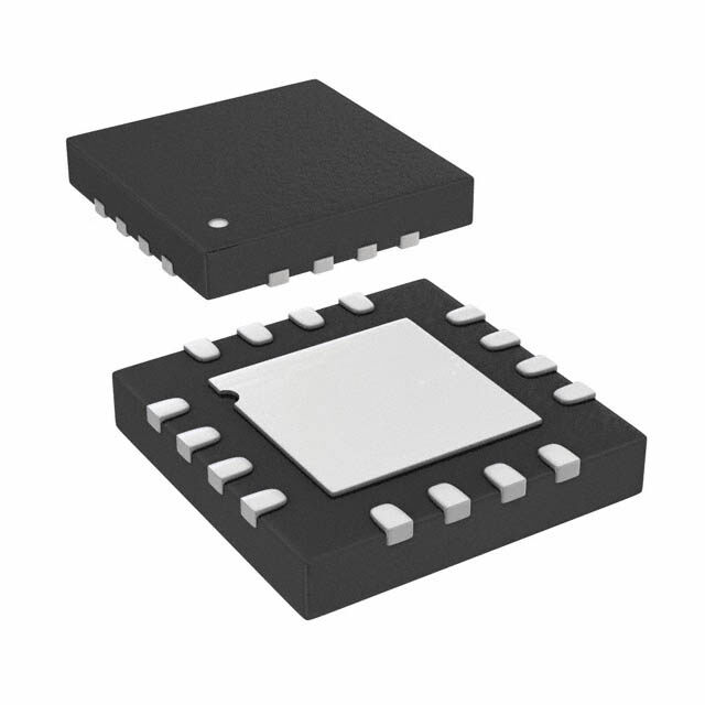
| 描述 | IC POT DGTL SGL 256POS 14-TSSOP数字电位计 IC IC 8-Bit SPI |
| 产品分类 | |
| 品牌 | Analog Devices Inc |
| 产品手册 | |
| 产品图片 |
|
| rohs | 符合RoHS无铅 / 符合限制有害物质指令(RoHS)规范要求 |
| 产品系列 | 数字电位计 IC,Analog Devices AD5260BRUZ20-RL7- |
| 数据手册 | |
| 产品型号 | AD5260BRUZ20-RL7 |
| POT数量 | Single |
| 产品种类 | 数字电位计 IC |
| 供应商器件封装 | 14-TSSOP |
| 其它名称 | AD5260BRUZ20-RL7DKR |
| 包装 | Digi-Reel® |
| 商标 | Analog Devices |
| 存储器类型 | 易失 |
| 安装类型 | 表面贴装 |
| 安装风格 | SMD/SMT |
| 容差 | 30 % |
| 封装 | Reel |
| 封装/外壳 | 14-TSSOP(0.173",4.40mm 宽) |
| 封装/箱体 | TSSOP-14 |
| 工作温度 | -40°C ~ 85°C |
| 工作电源电压 | 2.75 V |
| 工厂包装数量 | 1000 |
| 弧刷存储器 | Volatile |
| 抽头 | 256 |
| 接口 | 4 线 SPI(芯片选择) |
| 描述/功能 | Provide a single- or dual-channel, 256-position, digitally controlled variable resistor device |
| 数字接口 | SPI |
| 最大工作温度 | + 85 C |
| 最小工作温度 | - 40 C |
| 标准包装 | 1 |
| 每POT分接头 | 256 |
| 温度系数 | 标准值 35 ppm/°C |
| 电压-电源 | 4.5 V ~ 16.5 V, ±4.5 V ~ 5.5 V |
| 电源电压-最大 | 15 V |
| 电源电压-最小 | 5 V |
| 电源电流 | 25 uA |
| 电路数 | 1 |
| 电阻 | 20 kOhms |
| 电阻(Ω) | 20k |
| 系列 | AD5260 |
| 缓冲刷 | Buffered |


- 商务部:美国ITC正式对集成电路等产品启动337调查
- 曝三星4nm工艺存在良率问题 高通将骁龙8 Gen1或转产台积电
- 太阳诱电将投资9.5亿元在常州建新厂生产MLCC 预计2023年完工
- 英特尔发布欧洲新工厂建设计划 深化IDM 2.0 战略
- 台积电先进制程称霸业界 有大客户加持明年业绩稳了
- 达到5530亿美元!SIA预计今年全球半导体销售额将创下新高
- 英特尔拟将自动驾驶子公司Mobileye上市 估值或超500亿美元
- 三星加码芯片和SET,合并消费电子和移动部门,撤换高东真等 CEO
- 三星电子宣布重大人事变动 还合并消费电子和移动部门
- 海关总署:前11个月进口集成电路产品价值2.52万亿元 增长14.8%


PDF Datasheet 数据手册内容提取
1-/2-Channel 15 V Digital Potentiometer AD5260/AD5262 FEATURES FUNCTIONAL BLOCK DIAGRAMS 256 positions A W B AD5260: 1 channel AD5262: 2 channels (independently programmable) SHDN AD5260 Potentiometer replacement 20 kΩ, 50 kΩ, 200 kΩ VDD RDAC Low temperature coefficient: 35 ppm/°C VSS REGISTER 4-wire, SPI-compatible serial data input VL POWER-ON 5 V to 15 V single-supply; ±5.5 V dual-supply operation CS LOGIC RESET PR Power on midscale preset 8 APPLICATIONS CLK SERIAL INPUT REGISTER SDO Mechanical potentiometer replacement GSNDDI 02695-001 Instrumentation: gain, offset adjustment Figure 1. AD5260 Stereo channel audio level control A1 W1 B1 A2 W2 B2 Programmable voltage-to-current conversion Programmable filters, delays, time constants SHDN Line impedance matching Low resolution DAC replacement VDD RDAC1 RDAC2 GENERAL DESCRIPTION VSS REGISTER REGISTER The AD5260/AD5262 provide a single- or dual-channel, 256- VL position, digitally controlled variable resistor (VR) device.1 CS LOGIC PORWEESRE-TON PR These devices perform the same electronic adjustment function 8 as a potentiometer or variable resistor. Each channel of the CLK SERIAL INPUT REGISTER SDO AthDat5 t2a6p0s/ tAhDe 5fi2x6e2d croesnitsatoinrs v aa lfuixee adt rae psiositnotr dweittehr ma winiepde rb cyo an tact GSNDDI AD5262 02695-002 digital code loaded into the SPI-compatible serial-input register. Figure 2. AD5262 The resistance between the wiper and either end point of the edge of the CLK pin. The AD5262 address bit determines the fixed resistor varies linearly with respect to the digital code corresponding VR latch to be loaded with the last eight bits of transferred into the VR latch. The variable resistor offers a the data word during the positive edging of CS strobe. A serial completely programmable value of resistance, between the A data output pin at the opposite end of the serial register enables terminal and the wiper or the B terminal and the wiper. The simple daisy-chaining in multiple VR applications without fixed A-to-B terminal resistance of 20 Ω, 50 Ω, or 200 Ω has a additional external decoding logic. An optional reset pin (PR) nominal temperature coefficient of 35 ppm/°C. Unlike the forces the wiper to the midscale position by loading 0x80 into majority of the digital potentiometers in the market, these the VR latch. devices can operate up to 15 V or ±5 V provided proper supply The AD5260/AD5262 are available in thin surface-mount voltages are furnished. 14-lead TSSOP and 16-lead TSSOP packages. All parts are Each VR has its own VR latch that holds its programmed guaranteed to operate over the extended industrial temperature resistance value. These VR latches are updated from an internal range of −40°C to +85°C. serial-to-parallel shift register, which is loaded from a standard 3-wire serial-input digital interface. The AD5260 contains an 1 The terms digital potentiometers, VR, and RDAC are used interchangeably. 8-bit serial register whereas the AD5262 contains a 9-bit serial register. Each bit is clocked into the register on the positive Rev. A Information furnished by Analog Devices is believed to be accurate and reliable. However, no responsibility is assumed by Analog Devices for its use, nor for any infringements of patents or other One Technology Way, P.O. Box 9106, Norwood, MA 02062-9106, U.S.A. rights of third parties that may result from its use. Specifications subject to change without notice. No license is granted by implication or otherwise under any patent or patent rights of Analog Devices. Tel: 781.329.4700 www.analog.com Trademarks and registered trademarks are the property of their respective owners. Fax: 781.461.3113 ©2002–2010 Analog Devices, Inc. All rights reserved.
AD5260/AD5262 TABLE OF CONTENTS Features..............................................................................................1 Layout and Power Supply Bypassing.......................................18 Applications.......................................................................................1 Terminal Voltage Operating Range.........................................18 General Description.........................................................................1 Power-Up Sequence...................................................................18 Functional Block Diagrams.............................................................1 RDAC Circuit Simulation Model.............................................18 Revision History...............................................................................2 Macro Model Net List for RDAC.............................................18 Specifications.....................................................................................3 Applications Information..............................................................19 Electrical Characteristics—20 kΩ, 50 kΩ, 200 kΩ Versions..3 Bipolar DC or AC Operation from Dual Supplies.................19 Timing Diagrams..........................................................................5 Gain Control Compensation....................................................19 Absolute Maximum Ratings............................................................6 Programmable Voltage Reference............................................19 ESD Caution..................................................................................6 8-Bit Bipolar DAC......................................................................19 Pin Configurations and Function Descriptions...........................7 Bipolar Programmable Gain Amplifier...................................20 Typical Performance Characteristics.............................................9 Programmable Voltage Source with Boosted Output...........20 Test Circuits.....................................................................................14 Programmable 4 mA-to-20 mA Current Source...................20 Theory of Operation......................................................................15 Programmable Bidirectional Current Source.........................21 Digital Interfacing......................................................................15 Programmable Low-Pass Filter................................................21 Daisy-Chain Operation.............................................................16 Programmable Oscillator..........................................................21 RDAC Structure..........................................................................16 Resistance Scaling......................................................................22 Programming the Variable Resistor.........................................16 Outline Dimensions.......................................................................23 Programming the Potentiometer Divider...............................17 Ordering Guide..........................................................................24 REVISION HISTORY 8/10—Rev. 0 to Rev. A Changes to Figure 11 Caption and Figure 12................................9 Updated Format..................................................................Universal Changes to Figure 31......................................................................12 Deleted Figure 1; Renumbered Sequentially.................................1 Changes to Figure 35 Caption......................................................13 Changes to General Description Section......................................1 Changes to Figure 43 and Figure 46.............................................14 Changes to Conditions of Channel Resistance Matching Deleted Potentiometer Family Selection Guide.........................18 (AD5262 only) Parameter, Voltage Divider Temperature Change to Programmable Voltage Source with Boosted Output Coefficient Parameter, Full-Scale Error Parameter, and Zero- Section..............................................................................................20 Scale Error Parameter, Table 1........................................................3 Changes to Figure 64......................................................................21 Changes to Table 2 and Table 3.......................................................5 Updated Outline Dimensions.......................................................23 Changes to Table 4............................................................................6 Changes to Ordering Guide..........................................................24 Changes to Table 5............................................................................7 Changes to Table 6............................................................................8 3/02—Revision 0: Initial Version Rev. A | Page 2 of 24
AD5260/AD5262 SPECIFICATIONS ELECTRICAL CHARACTERISTICS—20 kΩ, 50 kΩ, 200 kΩ VERSIONS V = +15 V, V = 0 V, or V = +5 V, V = –5 V; V = +5 V; V = +5 V, V = 0 V, −40°C < T < +85°C, unless otherwise noted. DD SS DD SS L A B A The AD5260/AD5262 contain 1968 transistors. Die size: 89 mil × 105 mil (9345 sq mil). Table 1. Parameter Symbol Conditions Min Typ1 Max Unit DC CHARACTERISTICS RHEOSTAT MODE Specifications apply to all VRs Resistor Differential Nonlinearity2 R-DNL R , V = no connect −1 ±¼ +1 LSB WB A Resistor Nonlinearity2 R-INL R , V = no connect −1 ±½ +1 LSB WB A Nominal Resistor Tolerance3 ΔR T = 25°C −30 30 % AB A Resistance Temperature Coefficient ΔR /ΔT Wiper = no connect 35 ppm/°C AB Wiper Resistance R I = 1 V/R 60 150 Ω W W AB Channel Resistance Matching (AD5262 only) ΔR /R Channel 1 and Channel 2 R , 0.1 % WB WB WB D = 0x80 X Resistance Drift ΔR 0.05 % AB DC CHARACTERISTICS POTENTIOMETER DIVIDER MODE Specifications apply to all VRs Resolution N 8 Bits Differential Nonlinearity4 DNL −1 ±1/4 +1 LSB Integral Nonlinearity4 INL −1 ±1/2 +1 LSB Voltage Divider Temperature Coefficient ΔV /ΔT Code = half scale 5 ppm/°C W Full-Scale Error W Code = full scale −2 −1 +0 LSB FSE Zero-Scale Error V Code = zero scale 0 1 2 LSB WZSE RESISTOR TERMINALS Voltage Range5 V V V V A, B, W SS DD Ax and Bx Capacitance6 C f = 5 MHz, measured to GND, 25 pF A,B code = half scale Wx Capacitance6 C f = 1 MHz, measured to GND, 55 pF W code = half scale Common-Mode Leakage Current I V = V = V /2 1 nA CM A B DD Shutdown Current7 I 5 μA SHDN DIGITAL INPUTS and OUTPUTS Input Logic High V 2.4 V IH Input Logic Low V 0.8 V IL Input Logic High V V = 3 V, V = 0 V 2.1 V IH L SS Input Logic Low V V = 3 V, V = 0 V 0.6 V IL L SS Output Logic High (SDO) V R = 2 kΩ to 5 V 4.9 V OH PULL-UP Output Logic Low (SDO) V I = 1.6 mA, V = 5 V 0.4 V OL OL LOGIC Input Current8 I V = 0 V or 5 V ±1 μA IL IN Input Capacitance6 C 5 pF IL POWER SUPPLIES Logic Supply V 2.7 5.5 V L Power Single-Supply Range V V = 0 V 4.5 16.5 V DD RANGE SS Power Dual-Supply Range V ±4.5 ±5.5 V DD/SS RANGE Logic Supply Current I V = 5 V 60 μA L L Positive Supply Current I V = 5 V or V = 0 V 1 μA DD IH IL Negative Supply Current I V = −5 V 1 μA SS SS Power Dissipation9 P V = 5 V or V = 0 V, 0.3 mW DISS IH IL V = +5 V, V = –5 V DD SS Power Supply Sensitivity PSS ΔV = +5 V, ±10% 0.003 0.01 %/% DD Rev. A | Page 3 of 24
AD5260/AD5262 Parameter Symbol Conditions Min Typ1 Max Unit DYNAMIC CHARACTERISTICS6, 10 Bandwidth –3 dB BW R = 20 kΩ/50 kΩ/200 kΩ 310/130/30 kHz AB Total Harmonic Distortion THD V = 1 V , V = 0 V, f = 1 kHz, 0.014 % W A RMS B R = 20 kΩ AB V Settling Time t V = +5 V, V = −5 V, ±1 LSB 5 μs W S A B error band, R = 20 kΩ AB Crosstalk11 C V = V , V = 0 V, measure V 1 nV-sec T A DD B W with adjacent RDAC making full-scale code change (AD5262 only) Analog Crosstalk C V = V , V = 0 V, measure V –64 dB TA A1 DD B1 W1 with V = 5 V p-p at f = 10 kHz, W2 R = 20 kΩ/200 kΩ (AD5262 AB only) Resistor Noise Voltage eN_WB RWB = 20 kΩ, f = 1 kHz 13 nV/√Hz INTERFACE TIMING CHARACTERISTICS6, 12 Specifications apply to all parts Clock Frequency f 25 MHz CLK Input Clock Pulse Width t , t Clock level high or low 20 ns CH CL Data Setup Time t 10 ns DS Data Hold Time t 10 ns DH CLK to SDO Propagation Delay13 t R = 1 kΩ, C< 20 pF 1 160 ns PD L L CS Setup Time tCSS 5 ns CS High Pulse Width tCSW 20 ns Reset Pulse Width t 50 ns RS CLK Fall to CS Rise Hold Time tCSH 0 ns CS Rise to Clock Rise Setup tCS1 10 ns 1 Typical values represent average readings at 25°C and VDD = +5 V, VSS = −5 V. 2 Resistor position nonlinearity error (R-INL) is the deviation from an ideal value measured between the maximum resistance and the minimum resistance wiper positions. R-DNL measures the relative step change from ideal between successive tap positions. Parts are guaranteed monotonic. IW = VDD/R for both VDD = +5 V and VSS = −5V. 3 VAB = VDD, wiper = no connect. 4 INL and DNL are measured at VW with the RDAC configured as a potentiometer divider similar to a voltage output digital-to-analog converter. VA = VDD and VB = 0 V. DNL specification limits of ±1 LSB maximum are guaranteed monotonic operating conditions. 5 Resistor Terminal A, Terminal B, and Terminal W have no limitations on polarity with respect to each other. 6 Guaranteed by design and not subject to production test. 7 Measured at the Ax terminals. All Ax terminals are open-circuit in shutdown mode. 8 Worst-case supply current consumed when all logic-input levels set at 2.4 V, which is the standard characteristic of CMOS logic. 9 PDISS is calculated from (IDD × VDD). CMOS logic level inputs result in minimum power dissipation. 10 All dynamic characteristics use VDD = +5 V, VSS = −5 V, VL = +5 V. 11 Measured at VW where an adjacent VW is making a full-scale voltage change. 12 See Figure 5 for location of measured values. All input control voltages are specified with tR = tF = 2 ns (10% to 90% of 3 V) and timed from a voltage level of 1.5 V. Switching characteristics are measured using VL = 5 V. 13 Propagation delay depends on value of VDD, RL, and CL. Rev. A | Page 4 of 24
AD5260/AD5262 TIMING DIAGRAMS Table 2. AD5260 8-Bit Serial Data Word Format Data B7 (MSB) B6 B5 B4 B3 B2 B1 B0 (LSB) D7 D6 D5 D4 D3 D2 D1 D0 27 26 2 5 2 4 2 3 2 2 21 2 0 Table 3. AD5262 9-Bit Serial Data Word Format ADDR Data B8 B7 (MSB) B6 B5 B4 B3 B2 B1 B0 (LSB) A0 D7 D6 D5 D4 D3 D2 D1 D0 28 27 26 2 5 2 4 2 3 2 2 21 2 0 1 SDI D7 D6 D5 D4 D3 D2 D1 D0 0 1 CLK 0 1 RDAC REGISTER LOAD CS 0 VOUT 10 02695-004 Figure 3. AD5260 Timing Diagram 1 SDI A0 D7 D6 D5 D4 D3 D2 D1 D0 0 1 CLK 0 1 RDAC REGISTER LOAD CS 0 VOUT 10 02695-005 Figure 4. AD5262 Timing Diagram SDI 1 (DATA IN) Ax OR Dx Dx 0 t DS t DH 1 SDO A'x OR D'x D'x (DATA OUT) 0 t PD t 1 CH tCS1 CLK 0 tCL tCSH t 1 CSS CS tCSW 0 t S VOUTV0VDD ±1 LSB ERROR BRAND ±1 LSB02695-006 Figure 5. Detailed Timing Diagram t 1 RS PR 0 t V0DVD ±1 LSB ERROR BSAND ±1 LSBD02695-007 Figure 6. Preset Timing Diagram Rev. A | Page 5 of 24
AD5260/AD5262 ABSOLUTE MAXIMUM RATINGS T =25°C, unless otherwise noted. A Stresses above those listed under Absolute Maximum Ratings may cause permanent damage to the device. This is a stress Table 4. rating only; functional operation of the device at these or any Parameter Rating other conditions above those indicated in the operational V to GND −0.3 V to +17 V DD section of this specification is not implied. Exposure to absolute V to GND 0 V to −7 V SS maximum rating conditions for extended periods may affect V to V 17 V DD SS device reliability. V to GND 0 V to +7 V L VA, VB, VW to GND VSS, VDD AX to BX, AX to WX, BX to WX ESD CAUTION Intermittent1 ±20 mA Continuous ±5 mA Digital Inputs and Output Voltage −0.3 V to V + 0.3 V, or L to GND +7 V (whichever is less) Operating Temperature Range −40°C to +85°C Maximum Junction Temperature 150°C (T ) J MAX Storage Temperature Range −65°C to +150°C Lead Temperature (Soldering,10 sec) 300°C Vapor Phase (60 sec) 215°C Infrared (15 sec) 220°C Thermal Resistance2 θJA 14-Lead TSSOP 206°C/W 16-Lead TSSOP 150°C/W 1 Maximum terminal current is bounded by the maximum current handling of the switches, maximum power dissipation of the package, and maximum applied voltage across any two of the A, B, and W terminals at a given resistance setting. 2 Package power dissipation = (TJ MAX − TA)/θJA. Rev. A | Page 6 of 24
AD5260/AD5262 PIN CONFIGURATIONS AND FUNCTION DESCRIPTIONS A 1 14 SDO W 2 13 NC B 3 AD5260 12 VL TOP VIEW VDD 4 (Not to Scale) 11 VSS SHDN 5 10 GND CLK 6 9 PR SDI 7 8 CS NC = NO CONNECT 02695-008 Figure 7. AD5260 Pin Configuration Table 5. AD5260 Pin Function Descriptions Pin No. Mnemonic Description 1 A A Terminal. 2 W Wiper Terminal. 3 B B Terminal. 4 VDD Positive Power Supply. Specified for operation at both 5 V or 15 V (sum of |VDD| + |VSS| ≤ 15 V). 5 SHDN Active Low Input. Terminal A, open-circuit. Shutdown controls variable resistor. 6 CLK Serial Clock Input, Positive Edge Triggered. 7 SDI Serial Data Input. 8 CS Chip Select Input, Active Low. When CS returns high, data is loaded into the RDAC register. 9 PR Active Low Preset to Midscale. Sets RDAC registers to 0x80. 10 GND Ground. 11 VSS Negative Power Supply. Specified for operation from 0 V to −5 V. 12 VL Logic Supply Voltage. Needs to be the same voltage as the digital logic controlling the AD5260. 13 NC No Connect. Users should not connect anything other than a dummy pad on this pin. 14 SDO Serial Data Output. Open-drain transistor requires a pull-up resistor. Rev. A | Page 7 of 24
AD5260/AD5262 SDO 1 16 A2 A1 2 15 W2 W1 3 AD5262 14 B2 B1 4 TOP VIEW 13 VL (Not to Scale) VDD 5 12 VSS SHDN 6 11 GND CLK 7 10 PR SDI 8 9 CS 02695-009 Figure 8. AD5262 Pin Configuration Table 6. AD5262 Pin Function Descriptions Pin No. Mnemonic Description 1 SDO Serial Data Output. Open-drain transistor requires a pull-up resistor. 2 A1 A Terminal RDAC 1. 3 W1 Wiper RDAC 1, Address A0 = 0. 4 B1 B Terminal RDAC 1. 5 VDD Positive Power Supply. Specified for operation at both 5 V or 15 V. (Sum of |VDD| + |VSS| ≤ 15 V) 6 SHDN Active Low Input. Terminal A, open-circuit. Shutdown controls variable Resistor 1 through Resistor R2. 7 CLK Serial Clock Input, Positive Edge Triggered. 8 SDI Serial Data Input. 9 CS Chip Select Input, Active Low. When CS returns high, data in the serial input register is decoded, based on the Address Bit A0, and loaded into the target RDAC register. 10 PR Active Low Preset to Midscale. Sets RDAC registers to 0x80. 11 GND Ground. 12 VSS Negative Power Supply. Specified for operation at either 0 V or −5 V (sum of |VDD| + |VSS| < 15 V). 13 VL Logic Supply Voltage. Needs to be same voltage as the digital logic controlling the AD5262. 14 B2 B Terminal RDAC 2. 15 W2 Wiper RDAC 2, Address A0 = 1. 16 A2 A Terminal RDAC 2. Rev. A | Page 8 of 24
AD5260/AD5262 TYPICAL PERFORMANCE CHARACTERISTICS 0.8 0.5 L (LSB) 000...567 +5V E DNL (LSB) 000...234 TTTTAAAA ==== +++–42810552°°°5CCC°C RVVDSASDB === –+2550VVkΩ DE IN 0.4 MOD 0.1 O 0.3 R 0 M E STAT 0.2 ±5V +12V OMET –0.1 EO 0.1 NTI –0.2 H E R 0 OT –0.3 P –0.1 –0.4 +15V –0.2 0 32 64 9C6ODE 1(2D8ecima1l6)0 192 224 256 02695-010 –0.50 32 64 9C6ODE 1(2D8ecima1l6)0 192 224 256 02695-013 Figure 9. R-INL vs. Code vs. Supply Voltages Figure 12. DNL vs. Code 0.10 0.3 +5V 0.05 SB) 0.2 +±51V5V LSB) 0 NL (L 0.1 NL ( DE I E D –0.05 MO 0 AT MOD –0.10 METER –0.1 T O RHEOS –0.15 +5V OTENTI –0.2 –0.20 ±5V P –0.3 +12V +15V –0.25 –0.4 0 32 64 9C6ODE 1(2D8ecima1l6)0 192 224 256 02695-011 0 32 64 9C6ODE 1(D28ecima1l)60 192 224 25602695-014 Figure 10. R-DNL vs. Code vs. Supply Voltages Figure 13. INL vs. Code vs. Supply Voltages 1.0 0.5 0.8 VDD = +5V 0.4 ODE INL (LSB) 000...246 TA = +125°C TA = +85°C RVTSAASB = == – –24500Vk°CΩ ODE DNL (LSB) 000...123 ++±515V5VV M M R 0 R 0 E E T T ME –0.2 ME –0.1 O O TI –0.4 TI –0.2 N N OTE –0.6 TA = +25°C OTE –0.3 P P –0.8 –0.4 –1.0 –0.5 0 32 64 9C6ODE 1(D28ecima1l6)0 192 224 256 02695-012 0 32 64 9C6ODE 1(D28ecima1l)60 192 224 256 02695-015 Figure 11. INL vs. Code Figure 14. DNL vs. Code vs. Supply Voltages Rev. A | Page 9 of 24
AD5260/AD5262 1.0 2.5 B) AVG+3σ NL (LS 0.5 AVG 2.0 VDD/VSS=+15/0V E I D R MO 0 AVG–3σ LSB) 1.5 VDD/VSS=±5V TE E ( E S M F 1.0 O TI EN –0.5 VDD/VSS=+5V/0V T PO 0.5 –1.0 0 0 5 |VDD –1 V0SS| (V) 15 20 02695-016 –40 –20 0 TEM2P0ERATUR40E (°C) 60 80 100 02695-019 Figure 15. INL vs. Supply Voltages Figure 18. Full-Scale Error vs. Temperature 2.0 2.5 1.5 AVG+3σ 2.0 B) 1.0 NL (LS 0.5 AVG VDD/VSS=+5V/0V E I AVG–3σ B) 1.5 D S O 0 L TAT M –0.5 ZSE ( 1.0 VDD/VSS=±5V S O RHE –1.0 VDD/VSS=+15/0V 0.5 –1.5 –2.0 0 0 5 |VDD –1 V0SS| (V) 15 20 02695-017 –40 –20 0 TEM2P0ERATUR40E (°C) 60 80 100 02695-020 Figure 16. R-INL vs. Supply Voltages Figure 19. Zero-Scale Error vs. Temperature 124 1 RON @ VDD/VSS = +5V/0V SISTANCE (Ω) 1680444 RON @ VDD/VSS = +5V/–5V Y CURRENT (µA) 0.1 VVVLIIHLO ==G I05CVV = 5V E L R P R UP WIPE 44 RON @ VDD/VSS = +15V/0V /I SDSS 0.01 VDD/VSS = +15/0V D 24 I VDD/VSS = ±5V 4 0.001 –5 –1 3 VDD (V) 7 11 15 02695-018 –40 –7 TEM26PERATURE5 9(°C) 92 125 02695-021 Figure 17. Wiper On Resistance vs. Bias Voltage Figure 20. Supply Current vs. Temperature Rev. A | Page 10 of 24
AD5260/AD5262 28.0 120 C) 27.5 m/° 100 p O (p 80 27.0 C 20kΩ P 60 M (µA)C 26.5 VDD/VSS = +15/0V ODE TE 40 50kΩ GI M 20 ILO 26.0 VDD/VSS = ±5V ETER 0 25.5 OM TI –20 N E 200kΩ 25.0 OT –40 P 24.5 –60 –40 –7 TE2M6PERATURE5 (9°C) 92 125 02695-022 0 32 64 9C6ODE 1(D28ecima1l)60 192 224 256 02695-025 Figure 21. ILOGIC vs. Temperature Figure 24. Potentiometer Mode Tempco ΔVWB/ΔT vs. Code 1000 6 TA = 25°C CODE = 0xFF 0 0x80 –6 VVDLODG/VICS S= =5 V5V/0V –12 0x40 0x20 A) B) –18 (µOGIC 100 AIN (d –24 00xx0180 IL VDD/VSS = 5V/0V G –30 0x04 VLOGIC = 3V –36 0x02 –42 0x01 –48 10 –54 0 0.5 1.0 1.5 2.0 VI2H. 5(V) 3.0 3.5 4.0 4.5 5.0 02695-023 1k 10kFREQUENCY (Hz)100k 1M 02695-026 Figure 22. ILOGIC vs. Digital Input Voltage Figure 25. Gain vs. Frequency vs. Code, RAB = 20 kΩ 80 6 TA = 25°C CODE = 0xFF 70 0 C) 0x80 m/° 60 –6 p 0x40 CO (p 50 20kΩ –12 0x20 MP 40 B) –18 DE TE 30 50kΩ AIN (d –24 00xx0180 MO 20 G –30 T 0x04 STA 10 –36 0x02 O HE 0 –42 0x01 R –10 –48 200kΩ –20 –54 0 32 64 9C6ODE 1(D28ecima1l)60 192 224 256 02695-024 1k 10kFREQUENCY (Hz)100k 1M 02695-027 Figure 23. Rheostat Mode Tempco ΔRWB /ΔT vs. Code Figure 26. Gain vs. Frequency vs. Code, RAB = 50 kΩ Rev. A | Page 11 of 24
AD5260/AD5262 6 600 TA = 25°C CODE = 0xFF 0 0x80 500 –6 CODE 0xFF 0x40 –12 400 0x20 B) –18 A) N (d –24 0x10 (µC 300 GAI –30 0x08 LOGI VDD/VSS = ±5V I 0x04 200 –36 –42 0x02 VDD/VSS = +5V/0V 100 0x01 –48 CODE 0x55 –54 0 1k 10kFREQUENCY (Hz)100k 1M 02695-028 10k 100kFREQUENCY (Hz)1M 10M 02695-031 Figure 27. Gain vs. Frequency vs. Code, RAB = 200 kΩ Figure 30. ILOGIC vs. Frequency 6 60 f–3dB = 310kHz, R = 20kΩ CODE = 0x80, VA = VDD, VB = 0V 0 f–3dB = 131kHz, R = 50kΩ 50 –6 –PSRR @ VDD = ±5V DC ± 10% p-pAC –12 40 dB) –18 f–3dB = 30kHz, R = 200kΩ dB) N ( –24 R ( 30 GAI –30 PSR 20 –36 –42 10 +PSRR @ VDD = ±5V DC ± 10% p-pAC –48 –3dB VIN = 50mV rms BANDWIDTHS VDD/VSS= ±5V –54 0 1k 10kFREQUENCY (Hz)100k 1M 02695-029 100 1k FREQU1E0NkCY (Hz) 100k 1M 02695-032 Figure 28. −3 dB Bandwidth Figure 31. PSRR vs. Frequency 0.3 CODE = 0x80 0.2 VDD/VSS= ±5V dB) 0.1 TA = 25°C S ( ES 0 N R = 20kΩ 20mV/DIV T A –0.1 L F N –0.2 AI G D –0.3 R = 50kΩ E Z ALI –0.4 R = 200kΩ M R –0.5 NO 5V/DIV –0.6 –0.7 100 1kFREQUENCY (Hz)10k 100k 02695-030 1µs/DIV 02695-033 Figure 29. Normalized Gain Flatness vs. Frequency Figure 32. Midscale Glitch Energy, Code 0x80 to 0x7F Rev. A | Page 12 of 24
AD5260/AD5262 0.10 CODE = 0x80 %) VDD/VSS= ±5V E ( 0.05 SAMPLE SIZE = 135 UNITS C AVG – 3σ N A T S 0 SI E R NAL –0.05 AVG 5V/DIV MI R E N T –0.10 E I AVG + 3σ G N A –0.15 H C 5V/DIV –0.20 20µs/DIV 02695-034 0 50 100HO1U5R0S O2F00 OPE2R50ATIO3N00AT 315500°C400 450 500 02695-037 Figure 33. Large Signal Settling Time Figure 36. Long-Term Resistance Drift 40 CODE SET TO MIDSCALE TA = 150°C 3 LOTS SAMPLE SIZE = 135 UNITS 30 Y C N E U 20 10mV/DIV EQ R F 10 0 40ns/DIV 02695-035 –0.50 –0C.4H0AN–N0E.3L0-TO–-C0H.2A0NNE–0L. 1R0AB MA0TCH (%0).10 0.20 02695-038 Figure 34. Digital Feedthrough vs. Time Figure 37. Channel-to-Channel Resistance Matching (AD5262) 100 VA = VB = OPEN TA = 25°C A) 10 m (X A M B_ W L I 1 RAB = 20kΩ A C TI E R HEO 0.1 RAB = 50kΩ T RAB = 200kΩ 0.01 0 32 64 9C6ODE 1(D28ecima1l6)0 192 224 256 02695-036 Figure 35. Theoretical Maximum Current vs. Code Rev. A | Page 13 of 24
AD5260/AD5262 TEST CIRCUITS Figure 38 to Figure 46 define the test conditions used in Table 1. 0.1V DUT RW = IW CODE = 0x00 DUT V+ = VDD W 1LSB = V+/2N V+ A W B IW 0.1V B VMS02695-039 A = NC VSS TO VDD 02695-044 Figure 38. Potentiometer Divider Nonlinearity Error (INL, DNL) Figure 43. Incremental On Resistance NC NC NC = NO CONNECT DUT A W IW VDD A W ICM DUT B VMS 02695-040 VSS GND NCB VCM 02695-045 Figure 39. Resistor Position Nonlinearity Error Figure 44. Common-Mode Leakage Current (Rheostat Operation; R-INL, R-DNL) VLOGIC ILOGIC CS CLK DUT VMS2 A W VW IW= VDD/RNOMINAL SDI B DIGITAL INPUT VMS1 RW= (VMS1– VMS2)/IW 02695-041 VOLTAGE 02695-046 Figure 40. Wiper Resistance Figure 45. VLOGIC Current vs. Digital Input Voltage A1 VDD A2 VA V+ VDD A W PPVSS+ SR= R (V% (Dd/D%B ±)) ==1 02∆∆%0VV lMDoDSg%%(∆∆VVMDDS) VIN NC RWDA1BC11 VSS RDAWBC222 VOUT B VMS 02695-042 NCCTA = = N 2O0 lCoOg N(VNOEUCTT/VIN) 02695-047 Figure 41. Power Supply Sensitivity (PSS, PSSR) Figure 46. Analog Crosstalk A +13V W VIN DUT OFFSET AD8610 VOUT GND B –13V 02695-043 Figure 42. Gain vs. Frequency Rev. A | Page 14 of 24
AD5260/AD5262 THEORY OF OPERATION The AD5260/AD5262 provide a single- or dual-channel, 256- VL VDD position, digitally controlled variable resistor (VR) device and operate up to 15 V maximum voltage. Changing the programmed CS A1 VR settings is accomplished by clocking an 8-/9-bit serial data CLK RDAC W1 LATCH word into the SDI (serial data input) pin. For the AD5262, the 1 B1 format of this data word is one address bit. A0 represents the PR first bit, B8, followed by eight data bits, B7 to B0, with MSB SDI EN ADDR first. Table 2 and Table 3 provide the serial register data word A0 DEC format. See Table 7 for the AD5262 address assignment to decode SER REG the location of the VR latch receiving the serial register data in D7 D6 A2 Bit B7 through Bit B0. VR outputs can be changed one at a time D5 RDAC in random sequence. The AD5260/AD5262 preset to a midscale, D4 LATCH W2 D3 2 B2 simplifying fault condition recovery at power-up. Midscale can D2 SDO D1 PR also be achieved at any time by asserting the PR pin. Both parts D0 have an internal power-on preset that places the wiper in a POWER- PR SHDN midscale preset condition at power-on. Operation of the power- ON on preset function depends only on the state of the VL pin. GND PRESET VSS 02695-048 The AD5260/AD5262 contain a power shutdown SHDN pin Figure 47. AD5262 Block Diagram that places the RDAC in an almost zero power consumption The positive-edge sensitive CLK input requires clean transitions state where Terminals Ax are open circuited and the Wiper W to avoid clocking incorrect data into the serial input register. Stand- is connected to B, resulting in only leakage currents being con- ard logic families work well. If mechanical switches are used for sumed in the VR structure. In the shutdown mode, the VR latch product evaluation, they should be debounced by a flip-flop or settings are maintained so that, when returning to operational other suitable means. Figure 47 shows more detail of the inter- mode from power shutdown, the VR settings return to their nal digital circuitry. When CS is low, the clock loads data into previous resistance values. the serial input register on each positive clock edge (see Table 8). Table 7. AD5262 Address Decode Table Table 8. Truth Table1 A0 Latch Loaded CLK CS PR SHDN Register Activity 0 RDAC1 Low Low High High No SR effect, enables SDO pin. 1 RDAC2 ↑ Low High High Shift one bit in from the SDI pin. DIGITAL INTERFACING The eighth previously entered bit is shifted out of the SDO pin. The AD5260/AD5262 contain a 4-wire SPI-compatible digital X ↑ High High Load SR data into RDAC latch. interface (SDI, SDO, CS, and CLK). For the AD5260, the 8-bit X High High High No operation. serial word must be loaded with the MSB first. The format of X X Low High Sets all RDAC latches to half the word is shown in Table 2. For the AD5262, the 9-bit serial scale, wiper centered, and SDO word must be loaded with Address Bit A0 first, then the MSB latch cleared. of the data. The format of the word is shown in Table 3. X High ↑ High Latches all RDAC latches to 0x80. X High High Low Open circuits all Resistor A terminals, connects W to B, and turns off SDO output transistor. 1 ↑ = positive edge, X = don’t care, SR = shift register. The data setup and data hold times in Table 1 determine the data valid time requirements. The AD5260 uses an 8-bit serial input data register word that is transferred to the internal RDAC register when the CS line returns to logic high. For the AD5262, the last nine bits of the data word entered into the serial register are held when CS returns high. Any extra bits are ignored. At the same time CS goes high, it gates the address decoder, enabling one of two positive edge-triggered AD5262 RDAC latches (see Figure 48). Rev. A | Page 15 of 24
AD5260/AD5262 AD5260/AD5262 registers, and the CS pin is then pulled high to complete the CS RDAC1 ADDR operation. DECODE RDAC2 VDD CSLDKI RESGERISIATELR 02695-049 CONMTICRROOLL-ER ADU51260 R2.P2kΩ ADU52260 Figure 48. Equivalent Input Control Logic MOSI SDI SDO SDI SDO The target RDAC latch is loaded with the last eight bits of SCLK SS CS CLK CS CLK tAhDe 5se2r6i2a,l tdwaota s wepoarrda cteo m9-pbliet tdinatga o wnoer RdDs mACus ut pbde actleo.c Fkoerd t ihne to 02695-055 change both VR settings. Figure 52. Daisy-Chain Configuration During shutdown (SHDN), the SDO output pin is forced to the RDAC STRUCTURE off (logic high) state to disable power dissipation in the pull-up The RDAC contains a string of equal resistor segments with an resistor. See Figure 49 for the equivalent SDO output circuit array of analog switches that act as the wiper connection. The schematic. number of positions is the resolution of the device. The AD5260/ SHDN AD5262 have 256 connection points, allowing it to provide better SDO than 0.4% settability resolution. Figure 53 shows an equivalent CS structure of the connections between the three terminals that SDI RESGERISIATELR D Q make up one channel of the RDAC. SWA and SWB are always CK RS on, while one of the switches SW(0) to SW(2N – 1) is on one at a CLK PR 02695-050 tdiamtae ,b ditesp. eBnedcianugs eo tnh teh sew rietscihst iasn ncoe tp iodseiatilo, tnh dereec oisd ae d6 0fr Ωom w tipheer Figure 49. Detail SDO Output Schematic of the AD5260 resistance, R . Wiper resistance is a function of supply voltage W and temperature. The lower the supply voltage is, the higher the All digital inputs are protected with a series input resistor and wiper resistance becomes. Similarly, the higher the temperature parallel Zener ESD structure as shown in Figure 50. This applies is, the higher the wiper resistance becomes. Users should be to the CS, SDI, SDO, PR, SHDN, and CLK digital input pins. aware of the contribution of the wiper resistance when accurate 340Ω LOGIC prediction of the output resistance is needed. 02695-051 Ax Figure 50. ESD Protection of Digital Pins SHDN RS A, B, W D7 RS VSS 02695-052 DDD654 RS Figure 51. ESD Protection of Resistor Terminals D3 D2 DAISY-CHAIN OPERATION D1 D0 Wx The serial data output (SDO) pin contains an open-drain N- channel FET. This output requires a pull-up resistor to transfer data to the SDI pin of the next package. This allows for daisy- RDAC chaining several RDACs from a single processor serial data line. LATCH The pull-up resistor termination voltage can be larger than the AND VpfoeDlrlDoi oswdui pnwpghl yde envv ouilcsteain gigen. asI etp riuise lrsl-e bucepocm raeumssiesetn codarep tdao c ttiohti eivn eSc DlroeIaa dpseiinn tg ho eaf ttc htlhoece k DOIMGIITTDTAEELCD CO FIDROECRU CITLRARYRSITY RS = RAB/2N Bx 02695-056 Figure 53. Simplified RDAC Architecture daisy-chain node connecting SDO and SDI between devices PROGRAMMING THE VARIABLE RESISTOR may induce time delay to subsequent devices. Users should be aware of this potential problem to achieve data transfer Rheostat Operation successfully (see Figure 52). If two AD5260s are daisy-chained, The nominal resistances of the RDAC between Terminal A and this requires a total of 16 bits of data. The first eight bits, complying Terminal B are available with values of 20 kΩ, 50 kΩ, and 200 kΩ. with the format shown in Table 2, go to U2, and the second The final three digits of the part number determine the nominal eight bits with the same format go to U1. The CS pin should be resistance value, for example, 20 kΩ = 20, 50 kΩ = 50, 200 kΩ = kept low until all 16 bits are clocked into their respective serial 200. The nominal resistance (R ) of the VR has 256 contact points AB Rev. A | Page 16 of 24
AD5260/AD5262 accessed by the wiper terminal, plus the B terminal contact. The set for the RDAC latch codes shown in Table 10. The result is 8-bit data in the RDAC latch is decoded to select one of the 256 the same if Terminal B is tied to Terminal W. possible settings. Assuming a 20 kΩ part is used, the wiper’s first Table 10. R vs. Code WA connection starts at the B terminal for data 0x00. Because there RDAC (Dec) R (Ω) Output State WA is a 60 Ω wiper contact resistance, such a connection yields a 256 60 Full scale minimum of 60 Ω resistance between Terminal W and Terminal B. 128 10,060 Half scale The second connection is the first tap point corresponding to 1 19,982 1 LSB 138 Ω (R = R /256 R = 78 Ω + 60 Ω) for Data 0x01. The third WB AB W 0 20,060 Zero scale connection is the next tap point representing 216 Ω (78 × 2 + 60) 20 for Data 0x02, and so on. Each LSB data value increase moves RWA RWB the wiper up the resistor ladder until the last tap point is reached at 19,982 Ω (R − 1 LSB + R ). The wiper does not directly connect 16 AB W to the B terminal. See Figure 53 for a simplified diagram of the Ω k equivalent RDAC circuit. D) – 12 (B The general equation determining the digitally programmed W R output resistance between W and B is D), 8 ( A D W R (D)= ×R +R (1) R WB 256 AB W 4 where D is the decimal equivalent of the binary code that is RAB = 20kΩ loaded in the 8-bit RDAC register and R is the nominal end- AB 0 tFoo-re nexda rmespilset,a wnchee. n R = 20 kΩ, V = 0 V, and the A terminal is 0 64 CODE 1(D28ecimal) 192 256 02695-057 AB B Figure 54. AD5260/AD5262 Equivalent RDAC Circuit open circuit, the following output resistance values of R are WB set for the RDAC latch codes shown in Table 9. The result is the The typical distribution of the nominal resistance RAB from same if Terminal A is tied to W. channel to channel matches within ±1%. Device-to-device matching is process lot-dependent with the worst case of Table 9. RWB vs. Code ±30% variation. However, because the resistance element RDAC (Dec) RWB (Ω) Output State is processed in thin film technology, the change in RAB with 256 19,982 Full scale (R – 1 LSB + R ) temperature has a low 35 ppm/°C temperature coefficient. AB W 128 10,060 Midscale PROGRAMMING THE POTENTIOMETER DIVIDER 1 138 1 LSB 0 60 Zero-scale (wiper contact resistance) Voltage Output Operation Note that in the zero-scale condition, a finite wiper resistance of The digital potentiometer easily generates output voltages at 60 Ω is present. Care should be taken to limit the current flow wiper-to-B and wiper-to-A to be proportional to the input between W and B in this state to no more than 20 mA to avoid voltage at A-to-B. Ignore the effect of the wiper resistance. For degradation or possible destruction of the internal switches. example, connecting the A terminal to 5 V and the B terminal to ground produces an output voltage at W-to-B starting at 0 V Like the mechanical potentiometer the RDAC replaces, the up to 1 LSB less than 5 V. Each LSB of voltage is equal to the AD5260/AD5262 are completely symmetrical. The resistance voltage applied across Terminal A and Terminal B divided by between Wiper W and Terminal A also produces a digitally the 256 positions of the potentiometer divider. Because the controlled complementary resistance, R . Figure 54 shows the WA AD5260/AD5262 operate from dual supplies, the general symmetrical programmability of the various terminal connec- equation defining the output voltage at V with respect to tions. When R is used, the B terminal can be left floating or W WA ground for any given input voltage applied to Terminal A and tied to the wiper. Setting the resistance value for R starts at a WA Terminal B is maximum value of resistance and decreases as the data loaded in the latch is increased in value. The general equation for this D V (D)= ×V +V (3) operation is W 256 AB B 256−D Operation of the digital potentiometer in the divider mode R (D)= ×R +R (2) WA 256 AB W results in more accurate operation over temperature. Unlike the rheostat mode, the output voltage is dependent on the ratio of For example, when R = 20 kΩ, V = 0 V, and the B terminal is AB A the internal resistors, R and R , and not the absolute values; open circuit, the following output resistance values of R are WA WB WA therefore, the drift reduces to 5 ppm/°C. Rev. A | Page 17 of 24
AD5260/AD5262 LAYOUT AND POWER SUPPLY BYPASSING voltage range of the three terminals extends from V to V SS DD regardless of the digital input level. It is good practice to employ a compact, minimum lead length layout design. The leads to the input should be as direct as POWER-UP SEQUENCE possible with a minimum conductor length. Ground paths Because there are diodes to limit the voltage compliance at should have low resistance and low inductance. Terminal A, Terminal B, and Terminal W (see Figure 56), it is Similarly, it is also good practice to bypass the power supplies important to power V /V first before applying any voltage to DD SS with quality capacitors for optimum stability. Supply leads to the A, B, and W terminals. Otherwise, the diode becomes forward the device should be bypassed with 0.01 μF to 0.1 μF disc or biased such that V /V are powered unintentionally and may DD SS chip ceramic capacitors. Low ESR 1 μF to 10 μF tantalum or affect the rest of the user’s circuit. The ideal power-up sequence electrolytic capacitors should also be applied at the supplies to is in the following order: GND, V , V , V, the digital inputs, DD SS L minimize any transient disturbance (see Figure 55). Note that and V /V /V . The order of powering V /V /V and the digital A B W A B W the digital ground should also be joined remotely to the analog inputs is not important as long as they are powered after V /V . DD SS ground to minimize the ground bounce. RDAC CIRCUIT SIMULATION MODEL VDD + VDD The internal parasitic capacitances and the external capacitive C3 C1 10µF 0.1µF loads dominate the ac characteristics of the RDACs. Configured + as a potentiometer divider, the −3 dB bandwidth of the AD5260 C4 C2 VSS 10µF 0.1µF VSS GND (20 kΩ resistor) measures 310 kHz at half scale. Figure 28 provides 02695-053 trhesei slatorgr ev esirgsnioanl sB 2o0d ke Ωpl,o 5t0 c hkΩar,a acntedr i2s0ti0c sk oΩf .t Ahe p tahrraesei taicv asiilmabullea - Figure 55. Power Supply Bypassing tion model is shown in Figure 57. The following section provides a macro model net list for the 20 kΩ RDAC. TERMINAL VOLTAGE OPERATING RANGE RDAC The AD5260/AD5262 positive V and negative V power 20kΩ DD SS A B supply defines the boundary conditions for proper 3-terminal CW digital potentiometer operation. Supply signals present on the 25CpFA C25BpF A, B, and W terminals that exceed V or V are clamped by the internal forward-biased diodes (sDeDe FiguSrSe 5V6D)D. Figure 57. RDAC Circuit SimWu5l5aptFion Model02695-071 fo r RDAC 20 kΩ A MACRO MODEL NET LIST FOR RDAC W PARAM D=256, RDAC=20E3 * B VSS 02695-054 S*U BCKT DPOT ( A ,W,B) Figure 56. Maximum Terminal Voltages Set by VDD and VSS CA A 0 25E-12 RWA A W {(1-D/256)*RDAC+60} The ground pin of the AD5260/AD5262 device is primarily CW W 0 55E-12 used as a digital ground reference, which needs to be tied to the RWB W B {D/256*RDAC+60} common ground of the PCB. The digital input control signals to CB B 0 25E-12 the AD5260/AD5262 must be referenced to the device ground * pin (GND), and must satisfy the logic level defined in Table 1. .ENDS DPOT An internal level shift circuit ensures that the common-mode Rev. A | Page 18 of 24
AD5260/AD5262 APPLICATIONS INFORMATION BIPOLAR DC OR AC OPERATION FROM DUAL it avoids the ringing or oscillation at the worst case. For critical SUPPLIES applications, C2 should be found empirically to suit the need. In general, C2 in the range of a few picofarads (pF) to no more The AD5260/AD5262 can be operated from dual supplies than a few tenths of pF is usually adequate for the compensation. enabling control of ground referenced ac signals or bipolar Similarly, there are W and A terminal capacitances connected to operation. The ac signal, as high as V /V , can be applied DD SS the output (not shown). Fortunately, their effect at this node is less directly across Terminal A and Terminal B with output taken significant, and the compensation can be avoided in most cases. from Terminal W. See Figure 58 for a typical circuit connection. PROGRAMMABLE VOLTAGE REFERENCE +5.0V For voltage divider mode operation, shown in Figure 60, it is VDD SS CS VDD ±5V p-p common to buffer the output of the digital potentiometer unless MICROCONTROLLER SCLK CLK ±2.5V p-p the load is much larger than RWB. Not only does the buffer serve the purpose of impedance conversion, but it also allows a GND MOSI SDI D=0x80 heavier load to be driven. GND 5V VSS –5.0V 02695-058 1VIN U1 AD5260 5V Figure 58. Bipolar Operation from Dual Supplies VOUT 3 A W GAIN CONTROL COMPENSATION GND B AD8601 VO 2 AD1582 Digital potentiometers are commonly used in gain control as in the noninverting gain amplifier shown in Figure 59. A1 02695-060 C2 Figure 60. Programmable Voltage Reference 4.7pF 8-BIT BIPOLAR DAC R2 200kΩ Figure 61 shows a low cost 8-bit bipolar DAC. It offers the same B A R1 W number of adjustable steps but not the precision of conventional 47kΩ DACs. The linearity and temperature coefficients, especially at low C1 U1 VO values codes, are skewed by the effects of the digital potentiometer 25pF Vi 02695-059 wiper resistance. The output of this circuit is Figure 59. Typical Noninvertng Gain Amplifier ⎛2D ⎞ V =⎜ −1⎟×V (4) O ⎝256 ⎠ REF Note that when the RDAC B terminal parasitic capacitance is connected to the op amp noninverting node, it introduces a zero +5V AD5260 for the 1/β term with +20 dB/dec, whereas a typical op amp O gain bandwidth product (GBP) has −20 dB/dec characteristics. Vi U2 OP2177 VO A large R2 and finite C1 can cause this zero’s frequency to fall U1 W well below the crossover frequency. Therefore, the rate of VIN B A A2 –5V R R closure becomes 40 dB/dec and the system has 0 phase margin VOUT +5VREF W1 +5V –5VREF at the crossover frequency. The output may ring or oscillate if TRIM GND the input is a rectangular pulse or step function. Similarly, it is ADR425 also likely to ring when switching between two gain values OP2177 bDeecpaeunsde itnhgis o ins ethqeu iovpa laemntp t oG aB sPt,e rpe dcuhcainngge tahte t hfeee dinbpauctk. resistor A1 –5V 02695-061 Figure 61. 8-Bit Bipolar DAC may extend the zero’s frequency far enough to overcome the problem. A better approach, however, is to include a compensa- tion capacitor, C2, to cancel the effect caused by C1. Optimum compensation occurs when R1 × C1 = R2 × C2. This is not an option because of the variation of R2. As a result, the R1 × C1 = R2 × C2 relationship can be used, and scale C2 as if R2 is at its maximum value. Doing so may overcompensate and compromise the performance slightly when R2 is set at low values. However, Rev. A | Page 19 of 24
AD5260/AD5262 BIPOLAR PROGRAMMABLE GAIN AMPLIFIER PROGRAMMABLE VOLTAGE SOURCE WITH BOOSTED OUTPUT For applications that require bipolar gain, Figure 62 shows one implementation. Digital Potentiometer U1 sets the adjustment For applications that require high current adjustment such as a range. The wiper voltage at W2 can therefore be programmed laser diode driver or tunable laser, a boosted voltage source can between V and −KV at a given U2 setting. Configuring A2 in be considered (see Figure 63). i i the noninverting mode allows linear gain and attenuation. The Vi transfer function is VO 5V VVOi =⎜⎝⎛1+RR21⎟⎠⎞×⎜⎝⎛2D526×(1+K)−K⎟⎠⎞ (5) A W R1 10kΩ P1 CC RBIAS U1 N1 where K is the ratio of RWB1/RWA1 set by U1. B A1 SIGNAL LO IL VDD U1 = AD5260 ADU52262 OP2177 VO APN111 === FAFDDDPV8633060101,PN A,, ND2ND867S009504,23 A0D8541 02695-063 W2 R2 Figure 63. Programmable Boosted Voltage Source A2 B2 A2 C1 VSS In this circuit, the inverting input of the op amp forces VO to be Vi A1 WB11VDD –KVi R1 eloqauda lc tuor rtehnet wisi pthere nv odletaligvee rseedt bbyy tthhee dsuigpiptally pvoiate tnhteio Pm-cehtearn. nTehl e U1 FET, P1. The N-channel FET, N1, simplifies the op amp driving AD5262 requirement. A1 must be the rail-to-rail input type. Resistor R1 OP2177 is needed to prevent P1 from turning off once it is on. The choice A1 VSS 02695-062 othf eR o1u itsp au tb taularnnc-oe fbf ettiwmeee. nN t1h cea pno bwee ra nloys gs eonfe trhails- preusripstoosre asnigdn al Figure 62. Bipolar Programmable Gain Amplifier FET. However, P1 is driven in the saturation state, and there- fore, its power handling must be adequate to dissipate (V − V ) Similar to the previous example, in the simpler and more i O × I power. This circuit can source a maximum of 100 mA at 5 V common case, where K = 1, with a single digital potentiometer, L supply. Higher current can be achieved with P1 in a larger pack- AD5260, U1 is replaced by a matched pair of resistors to apply age. Note that a single N-channel FET can replace P1, N1, and V and −V at the ends of the digital potentiometer. The relation- i i R1 altogether. However, the output swing is limited unless sepa- ship becomes rate power supplies are used. For a precision application, a V =⎜⎛1+R2⎟⎞⎜⎛2D2−1⎟⎞×V (6) voltage reference such as the ADR423, ADR292, or AD1584 can O ⎝ R1⎠⎝ 256 ⎠ i be applied at the input of the digital potentiometer. If R2 is large, a few picofarad compensation capacitors may be PROGRAMMABLE 4 mA-TO-20 mA CURRENT needed to avoid any gain peaking. SOURCE Table 11 shows the result of adjusting D, with A2 configured as A programmable 4 mA-to-20 mA current source can be a unity gain, a gain of 2, and a gain of 10. The result is a bipolar implemented with the circuit shown in Figure 64. REF191 is a amplifier with linearly programmable gain and 256-step unique low supply headroom and high current handling resolution. precision reference that can deliver 20 mA at 2.048 V. The load current is simply the voltage across Terminal B to Terminal W Table 11. Result of Bipolar Gain Amplifier of the digital potentiometer, divided by R. D R1 = ∞, R2 = 0 R1 = R2 R2 = 9 × R1 S 0 −1 −2 −10 I =VREF×D (7) 64 −0.5 −1 −5 L R S 128 0 0 0 192 +0.5 +1 +5 255 +0.968 +1.937 +9.680 Rev. A | Page 20 of 24
AD5260/AD5262 +5V 1 1 Q= + (11) R1C1 R2C2 2 U1 VS Users can first select any convenient value for the capacitors. To REF191 3 SLEEP 0V TO (2.048V + VL) achieve maximally flat bandwidth where Q = 0.707, let C1 be 6 OUTPUT twice the size of C2 and let R1 = R2. As a result, users can adjust GND 1µCF1 AD5260 B W R1 and R2 to the same settings to achieve the desirable bandwidth. 4 A +5V C1 U2 – RS +2.5V OP1177 102Ω R1 R2 –2.048 TO VL –5V+ R10L0Ω VLIL 02695-064 Vi AR WB AR WB AD8601 VO Figure 64. Programmable 4-to-20 mA Current Source C2 –2.5V Tidheea lc bireccuaiut sies sthime pglreo, ubnudt bpeo taewnatirael tohfa Rt EduFa1l9-1su cpapnl ys woipn agm frposm a re SAADMJEU SSETTETDI NTGOS 02695-066 −2.048 V at zero scale to VL at full scale of the potentiometer Figure 66. Sallen Key Low-Pass Filter setting. Although the circuit works under single supply, the PROGRAMMABLE OSCILLATOR programmable resolution of the system is reduced. In a classic Wien-bridge oscillator (see Figure 67), the Wien PROGRAMMABLE BIDIRECTIONAL CURRENT network (R, R’, C, C’) provides positive feedback, whereas R1 SOURCE and R2 provide negative feedback. At the resonant frequency, f, o For applications that require bidirectional current control or the overall phase shift is zero, and the positive feedback causes higher voltage compliance, a Howland current pump can be a the circuit to oscillate. With R = R’, C = C’, and R2 = R2A//(R2B + solution (see Figure 65). If the resistors are matched, the load R ), the oscillation frequency is DIODE current is 1 1 ω = or f = (12) (R2A+R2B) R1 O RC O 2πRC I = ×V (8) L R2B W where R is equal to R such that WA R1' R2' 150kΩ 15kΩ 256−D R= R (13) 256 AB C1 At resonance, setting 10pF +15V R2 =2 (14) C2 A2 R1 +5V 10pF AD8016 +15V balances the bridge. In practice, R2/R1 should be set slightly A RL larger than 2 to ensure the oscillation can start. However, the 50Ω AD5260 15R01kΩ –15V alternate turn-on of the diodes, D1 and D2, ensures R2/R1 to W OP2177 VL be smaller than 2 momentarily and therefore stabilizes the B R2A 14.95kΩ RL oscillation. A1 500Ω –5V –15V IL 02695-065 Wtunheedn bthy eR f2rBeq bueecnacuys eis set, the oscillation amplitude can be Figure 65. Programmable Bidirectional Current Source 2 PROGRAMMABLE LOW-PASS FILTER V =I R2B+V (15) 3 O D D Digital Potentiometer AD5262 can be used to construct a V , I , and V are interdependent variables. With proper second-order, Sallen-Key low-pass filter (see Figure 66). The O D D selection of R2B, an equilibrium is reached such that V design equations are O converges. R2B can be in series with a discrete resistor to V ω 2 increase the amplitude, but the total resistance cannot be too O = O (9) V ω large to saturate the output. i S2 + O S+ω 2 Q O In both circuits in Figure 66 and Figure 67, the frequency tuning requires that both RDACs be adjusted to the same settings. 1 ωO = R1R2C1C2 (10) Because the two channels are adjusted one at a time, an intermedi- Rev. A | Page 21 of 24
AD5260/AD5262 ate state occurs that may not be acceptable for certain applications. In voltage divider mode, a much lower resistance can be achieved As a result, different devices can also be used in daisy-chained by paralleling a discrete resistor as shown in Figure 69. The mode so that parts can be programmed to the same setting equivalent resistance becomes simultaneously. D R = (R1//R2)+R (16) FREQUENCY WB_eq 256 W ADJUSTMENT C' R' VP 2.2nF 10kΩ ⎛ D ⎞ C RB +5V AW B RWA_eq =⎜⎝1−256⎟⎠(R1//R2)+RW (17) 2.2nF 10kΩ W A A U1 OP1177 VO AD5262 W R2 R1 R1 = R1' = R2B = AD5262 D1 = D2 = 1N4148 –5V VN R2A 2.1kΩ D1 R1 B1R02kBΩA D2 R2<<RB1 02695-069 1kΩ W Figure 69. Lowering the Nominal Resistance AADMJPULSITTUMDEENT 02695-067 Fchigaunrgee 6 s8t eapnsd lFinigeuarrley .6 H9 oshwoewv etrh,a lto tgh eta dpiegrit aadl pjuosttemnteionmt iest uerssu ally Figure 67. Programmable Oscillator with Amplitude Control preferred in applications like audio control. Figure 70 shows RESISTANCE SCALING another method of resistance scaling. In this circuit, the smaller The AD5260/AD5262 offer 20 kΩ, 50 kΩ, and 200 kΩ nominal R2 is with respect to RAB, the more the pseudo-log taper resistance. For users who need lower resistance and still main- characteristic behaves. tain the numbers of step adjustment, they can place multiple Vi devices in parallel. For example, Figure 68 shows a simple scheme of paralleling both channels of the AD5262. To adjust A W R1 VO half of the resistance linearly per step, users need to program B R2 both channels coherently with the same settings. VDD 02695-070 Figure 70. Resistor Scaling with Log Adjustment Characteristics A1 A2 W1 W2 B1 B2 LD 02695-068 Figure 68. Reduce Resistance by Half with Linear Adjustment Characteristics Rev. A | Page 22 of 24
AD5260/AD5262 OUTLINE DIMENSIONS 5.10 5.00 4.90 14 8 4.50 4.40 6.40 BSC 4.30 1 7 PIN 1 0.65 BSC 1.05 1.00 1M.2A0X 0.20 0.80 0.09 0.75 0.15 8° 0.60 0.05 0.30 SPELAATNIENG 0° 0.45 COPLANARITY 0.19 0.10 COMPLIANT TO JEDEC STANDARDS MO-153-AB-1 061908-A Figure 71. 14-Lead Thin Shrink Small Outline Package [TSSOP] (RU-14) Dimensions shown in millimeters 5.10 5.00 4.90 16 9 4.50 6.40 4.40 BSC 4.30 1 8 PIN 1 1.20 MAX 0.15 0.20 0.05 0.09 0.75 0.30 8° 0.60 B0.S6C5 0.19 SEATING 0° 0.45 PLANE COPLANARITY 0.10 COMPLIANT TO JEDEC STANDARDS MO-153-AB Figure 72. 16-Lead Thin Shrink Small Outline Package [TSSOP] (RU-16) Dimensions shown in millimeters Rev. A | Page 23 of 24
AD5260/AD5262 ORDERING GUIDE Model1 RAB (kΩ) Temperature Package Description Package Option No. of Parts per Container AD5260BRUZ20 20 −40°C to +85°C 14-Lead TSSOP RU-14 96 AD5260BRUZ20-RL7 20 −40°C to +85°C 14-Lead TSSOP RU-14 1000 AD5260BRUZ50 50 −40°C to +85°C 14-Lead TSSOP RU-14 96 AD5260BRUZ50-REEL7 50 −40°C to +85°C 14-Lead TSSOP RU-14 1000 AD5260BRUZ200 200 −40°C to +85°C 14-Lead TSSOP RU-14 96 AD5260BRUZ200-RL7 200 −40°C to +85°C 14-Lead TSSOP RU-14 1000 AD5262BRU20 20 −40°C to +85°C 16-Lead TSSOP RU-16 96 AD5262BRU20-REEL7 20 −40°C to +85°C 16-Lead TSSOP RU-16 1000 AD5262BRU50 50 −40°C to +85°C 16-Lead TSSOP RU-16 96 AD5262BRU50-REEL7 50 −40°C to +85°C 16-Lead TSSOP RU-16 1000 AD5262BRU200 200 −40°C to +85°C 16-Lead TSSOP RU-16 96 AD5262BRU200-REEL7 200 −40°C to +85°C 16-Lead TSSOP RU-16 1000 AD5262BRUZ20 20 −40°C to +85°C 16-Lead TSSOP RU-16 96 AD5262BRUZ20-RL7 20 −40°C to +85°C 16-Lead TSSOP RU-16 1000 AD5262BRUZ50 50 −40°C to +85°C 16-Lead TSSOP RU-16 96 AD5262BRUZ50-RL7 50 −40°C to +85°C 16-Lead TSSOP RU-16 1000 AD5262BRUZ200 200 −40°C to +85°C 16-Lead TSSOP RU-16 96 AD5262BRUZ200-RL7 200 −40°C to +85°C 16-Lead TSSOP RU-16 1000 EVAL-AD5262EBZ Evaluation Board 1 Z = RoHS Compliant Part. ©2002–2010 Analog Devices, Inc. All rights reserved. Trademarks and registered trademarks are the property of their respective owners. D02695-0-8/10(A) Rev. A | Page 24 of 24
Mouser Electronics Authorized Distributor Click to View Pricing, Inventory, Delivery & Lifecycle Information: A nalog Devices Inc.: EVAL-AD5262EBZ AD5260BRUZ50 AD5260BRUZ200 AD5262BRU20 AD5262BRUZ50 AD5262BRUZ200 AD5260BRUZ20 AD5262BRUZ20 AD5262BRU200 AD5262BRU50 AD5260BRUZ200-RL7 AD5260BRUZ20-RL7 AD5260BRUZ50-REEL7 AD5262BRU20-REEL7 AD5262BRU50-REEL7 AD5262BRUZ200-RL7 AD5262BRUZ20- RL7 AD5262BRUZ50-RL7