ICGOO在线商城 > 集成电路(IC) > 线性 - 放大器 - 仪表,运算放大器,缓冲器放大器 > AD524AD
 Datasheet下载
- 型号: AD524AD
- 制造商: Analog
- 库位|库存: xxxx|xxxx
- 要求:
| 数量阶梯 | 香港交货 | 国内含税 |
| +xxxx | $xxxx | ¥xxxx |
查看当月历史价格
查看今年历史价格
AD524AD产品简介:
ICGOO电子元器件商城为您提供AD524AD由Analog设计生产,在icgoo商城现货销售,并且可以通过原厂、代理商等渠道进行代购。 AD524AD价格参考¥293.81-¥386.48。AnalogAD524AD封装/规格:线性 - 放大器 - 仪表,运算放大器,缓冲器放大器, 仪表 放大器 1 电路 16-CDIP。您可以下载AD524AD参考资料、Datasheet数据手册功能说明书,资料中有AD524AD 详细功能的应用电路图电压和使用方法及教程。
AD524AD 是由 Analog Devices Inc. 生产的一款高性能仪表放大器,属于线性 - 放大器 - 仪表、运算放大器、缓冲器放大器类别。该型号在以下应用场景中具有广泛的应用价值:

1. 医疗设备:
   AD524AD 可用于心电图(ECG)、脑电图(EEG)和肌电图(EMG)等医疗监测设备中。它能够高精度地放大微弱的生物电信号,同时抑制共模干扰信号,确保数据的准确性和可靠性。

2. 工业自动化与控制:
   在工业领域,AD524AD 常用于传感器信号调理电路中。例如,压力传感器、温度传感器或应变片输出的微小信号可以通过 AD524AD 进行放大,以适应后续 ADC 或控制系统的需求。

3. 精密测量仪器:
   该芯片适用于需要高增益精度和低噪声特性的精密测量仪器,如电子秤、数据采集系统和测试设备。其出色的共模抑制比(CMRR)使其能够在复杂电磁环境中保持稳定的性能。

4. 音频处理:
   AD524AD 的低失真特性使其适合用于高品质音频信号的放大,尤其是在需要高信噪比和低失真的场景中,例如专业音响设备或录音设备。

5. 航空航天与国防:
   在对可靠性和精度要求极高的航空航天和国防应用中,AD524AD 被用来处理导航系统、雷达信号或其他关键任务中的微弱信号。

6. 汽车电子:
   在现代汽车中,AD524AD 可用于胎压监测系统(TPMS)、发动机控制单元(ECU)以及各种传感器信号的处理,提供稳定且精确的信号放大功能。

总结来说,AD524AD 凭借其卓越的性能指标(如高 CMRR、低输入偏置电流和宽增益范围),成为许多高精度、低噪声应用的理想选择。
| 参数 | 数值 |
| -3db带宽 | 1MHz |
| 产品目录 | 集成电路 (IC)半导体 |
| 描述 | IC OPAMP INSTR 1MHZ 16CDIP仪表放大器 IC PREC |
| 产品分类 | Linear - Amplifiers - Instrumentation, OP Amps, Buffer Amps集成电路 - IC |
| 品牌 | Analog Devices |
| 产品手册 | |
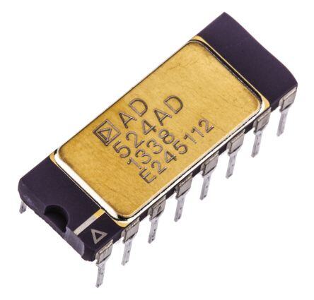
| 产品图片 |
|
| rohs | 否不符合限制有害物质指令(RoHS)规范要求 |
| 产品系列 | 放大器 IC,仪表放大器,Analog Devices AD524AD- |
| 数据手册 | |
| 产品型号 | AD524AD |
| 产品培训模块 | http://www.digikey.cn/PTM/IndividualPTM.page?site=cn&lang=zhs&ptm=30008http://www.digikey.cn/PTM/IndividualPTM.page?site=cn&lang=zhs&ptm=26202 |
| 产品种类 | 仪表放大器 |
| 供应商器件封装 | 16-CDIP 侧面铜焊 |
| 共模抑制比—最小值 | 110 dB |
| 包装 | 管件 |
| 压摆率 | 5 V/µs |
| 双重电源电压 | +/- 15 V |
| 可用增益调整 | 1 V/V to 1000 V/V |
| 商标 | Analog Devices |
| 增益带宽生成 | 25 MHz |
| 增益带宽积 | 1MHz |
| 安装类型 | 通孔 |
| 安装风格 | Through Hole |
| 封装 | Tube |
| 封装/外壳 | 16-CDIP(0.300",7.62mm) |
| 封装/箱体 | CERDIP-16 |
| 工作温度 | -25°C ~ 85°C |
| 工作温度范围 | - 40 C to + 85 C |
| 工作电源电压 | 15 V |
| 工厂包装数量 | 23 |
| 带宽 | 400 kHz |
| 放大器类型 | 仪表 |
| 最大功率耗散 | 450 mW |
| 最大工作温度 | + 85 C |
| 最大输入电阻 | 1000 MOhms |
| 最小工作温度 | - 40 C |
| 标准包装 | 23 |
| 电压-电源,单/双 (±) | ±6 V ~ 18 V |
| 电压-输入失调 | 250µV |
| 电流-电源 | 3.5mA |
| 电流-输入偏置 | 50nA |
| 电流-输出/通道 | - |
| 电源电流 | 3.5 mA |
| 电路数 | 1 |
| 系列 | AD524 |
| 视频文件 | http://www.digikey.cn/classic/video.aspx?PlayerID=1364138032001&width=640&height=505&videoID=2245193153001http://www.digikey.cn/classic/video.aspx?PlayerID=1364138032001&width=640&height=505&videoID=2245193159001 |
| 转换速度 | 5 V/us |
| 输入偏压电流—最大 | 50 nA |
| 输入补偿电压 | 250 uV |
| 输出类型 | - |
| 通道数量 | 1 Channel |


- 商务部:美国ITC正式对集成电路等产品启动337调查
- 曝三星4nm工艺存在良率问题 高通将骁龙8 Gen1或转产台积电
- 太阳诱电将投资9.5亿元在常州建新厂生产MLCC 预计2023年完工
- 英特尔发布欧洲新工厂建设计划 深化IDM 2.0 战略
- 台积电先进制程称霸业界 有大客户加持明年业绩稳了
- 达到5530亿美元!SIA预计今年全球半导体销售额将创下新高
- 英特尔拟将自动驾驶子公司Mobileye上市 估值或超500亿美元
- 三星加码芯片和SET,合并消费电子和移动部门,撤换高东真等 CEO
- 三星电子宣布重大人事变动 还合并消费电子和移动部门
- 海关总署:前11个月进口集成电路产品价值2.52万亿元 增长14.8%


PDF Datasheet 数据手册内容提取
Precision Instrumentation Amplifier Data Sheet AD524 FEATURES FUNCTIONAL BLOCK DIAGRAM Low noise: 0.3 μV p-p at 0.1 Hz to 10 Hz Low nonlinearity: 0.003% (G = 1) – INPUT 1 PROTECTION High CMRR: 120 dB (G = 1000) 4.44kΩ AD524 G = 10 13 Low offset voltage: 50 μV 404Ω Low offset voltage drift: 0.5 μV/°C G = 100 12 Vb 20kΩ Gain bandwidth product: 25 MHz G = 1000 11 40Ω SENSE Pin programmable gains of 1, 10, 100, 1000 RG1 16 20kΩ 20kΩ OUTPUT Input protection, power-on/power-off RG2 3 20kΩ 20kΩ No external components required 20kΩ REFERENCE Internally compensated M16I-Ll-eSaTdD c-e8r8a3mBi ac nDdIP c hainpds SaOvaICil apbalcek ages and 20-terminal + INPUT 2 PROTECTION 00500-001 Figure 1. leadless chip carrier available Available in tape and reel in accordance with EIA-481A standard Standard military drawing also available GENERAL DESCRIPTION The AD524 is a precision monolithic instrumentation amplifier PRODUCT HIGHLIGHTS designed for data acquisition applications requiring high accu- 1. Guaranteed low offset voltage, low offset voltage drift, and racy under worst-case operating conditions. An outstanding low noise for precision high gain applications. combination of high linearity, high common-mode rejection, 2. Functionally complete with pin programmable gains of 1, low offset voltage drift, and low noise makes the AD524 suitable 10, 100, and 1000, and single resistor-programmable for for use in many data acquisition systems. The AD524 has an any gain. output offset voltage drift of less than 25 μV/°C, input offset 3. Input and output offset nulling terminals are provided for voltage drift of less than 0.5 μV/°C, CMR above 90 dB at unity high precision applications and to minimize offset voltage gain (120 dB at G = 1000), and maximum nonlinearity of changes in gain ranging applications. 0.003% at G = 1. The gain bandwidth product of the AD524 is 4. Input protected for both power-on and power-off fault 25 kHz (G = 1000). The output slew rate of 5 V/μs and settling conditions. time of 15 μs to 0.01% for gains of 1 to 100, makes it suitable for 5. Superior dynamic performance with a gain bandwidth high speed data acquisition systems. product of 25 MHz, full power response of 75 kHz and a As a complete amplifier, the AD524 does not require any external settling time of 15 μs to 0.01% of a 20 V step (G = 100). components for fixed gains of 1, 10, 100, and 1000. For other gain settings between 1 and 1000, only a single resistor is required. The AD524 input is fully protected for both power-on and power-off fault conditions. The AD524 is available in four versions of accuracy and operating temperature range. The economical A grade, the low drift B grade, and lower drift, higher linearity C grade are specified from −25°C to +85°C. The S grade guarantees performance to specification over the extended temperature range −55°C to +125°C. The AD524 is available in a 16-lead ceramic DIP, 16-lead SBDIP, 16-lead SOIC wide packages, and 20-terminal leadless chip carrier. Rev. G Document Feedback Information furnished by Analog Devices is believed to be accurate and reliable. However, no responsibility is assumed by Analog Devices for its use, nor for any infringements of patents or other One Technology Way, P.O. Box 9106, Norwood, MA 02062-9106, U.S.A. rights of third parties that may result from its use. Specifications subject to change without notice. No license is granted by implication or otherwise under any patent or patent rights of Analog Devices. Tel: 781.329.4700 ©1983–2018 Analog Devices, Inc. All rights reserved. Trademarks and registered trademarks are the property of their respective owners. Technical Support www.analog.com
AD524 Data Sheet TABLE OF CONTENTS Features .............................................................................................. 1 Input Offset and Output Offset ................................................ 15 Functional Block Diagram .............................................................. 1 Gain .............................................................................................. 16 General Description ......................................................................... 1 Input Bias Currents .................................................................... 17 Product Highlights ........................................................................... 1 Common-Mode Rejection ........................................................ 17 Revision History ............................................................................... 2 Grounding ................................................................................... 18 Specifications ..................................................................................... 3 Sense Terminal ............................................................................ 18 Absolute Maximum Ratings ............................................................ 8 Reference Terminal .................................................................... 18 Connection Diagrams .................................................................. 8 Programmable Gain ................................................................... 20 ESD Caution .................................................................................. 8 Auto-Zero Circuits ..................................................................... 20 Typical Performance Characteristics ............................................. 9 Error Budget Analysis ................................................................ 21 Test Circuits ................................................................................. 14 References .................................................................................... 23 Theory of Operation ...................................................................... 15 Outline Dimensions ....................................................................... 24 Input Protection .......................................................................... 15 Ordering Guide .......................................................................... 25 REVISION HISTORY 1/2018—Rev. F to Rev. G Changes to General Description .................................................... 1 Change to Output Offset Voltage vs. Temperature Parameter, Unit Column, Table 1 ....................................................................... 3 Added References Section ............................................................. 23 Updated Outline Dimensions ....................................................... 24 Changes to Ordering Guide .......................................................... 25 11/2007—Rev. E to Rev. F Updated Format .................................................................. Universal Changes to General Description .................................................... 1 Changes to Figure 1 .......................................................................... 1 Changes to Figure 3 and Figure 4 Captions .................................. 8 Changes to Error Budget Analysis Section ................................. 21 Changes to Ordering Guide .......................................................... 25 4/1999—Rev. D to Rev. E Rev. G | Page 2 of 25
Data Sheet AD524 SPECIFICATIONS At V = ±15 V, R = 2 kΩ and T = +25°C, unless otherwise noted. S L A All min and max specifications are guaranteed. Specifications shown in boldface are tested on all production units at the final electrical test. Results from those tests are used to calculate outgoing quality levels. Table 1. AD524A AD524B Parameter Min Typ Max Min Typ Max Unit GAIN Gain Equation (External Resistor Gain Programming) 40,000 40,000 +1±20% +1±20% RG RG Gain Range (Pin Programmable) 1 to 1000 1 to 1000 Gain Error1 G = 1 ±0.05 ±0.03 % G = 10 ±0.25 ±0.15 % G = 100 ±0.5 ±0.35 % G = 1000 ±2.0 ±1.0 % Nonlinearity G = 1 ±0.01 ±0.005 % G = 10, G = 100 ±0.01 ±0.005 % G = 1000 ±0.01 ±0.01 % Gain vs. Temperature G = 1 5 5 ppm/°C G = 10 15 10 ppm/°C G = 100 35 25 ppm/°C G = 1000 100 50 ppm/°C VOLTAGE OFFSET (May be Nulled) Input Offset Voltage 250 100 µV vs. Temperature 2 0.75 µV/°C Output Offset Voltage 5 3 mV vs. Temperature 100 50 µV/°C Offset Referred to the Input vs. Supply G = 1 70 75 dB G = 10 85 95 dB G = 100 95 105 dB G = 1000 100 110 dB INPUT CURRENT Input Bias Current ±50 ±25 nA vs. Temperature ±100 ±100 pA/°C Input Offset Current ±35 ±15 nA vs. Temperature ±100 ±100 pA/°C Rev. G | Page 3 of 25
AD524 Data Sheet AD524A AD524B Parameter Min Typ Max Min Typ Max Unit INPUT Input Impedance Differential Resistance 109 109 Ω Differential Capacitance 10 10 pF Common-Mode Resistance 109 109 Ω Common-Mode Capacitance 10 10 pF Input Voltage Range Maximum Differential Input Linear (V )2 ±10 ±10 V DL Maximum Common-Mode Linear (VCM)2 G G V 12V− ×V 12V− ×V 2 D 2 D Common-Mode Rejection DC to 60 Hz with 1 kΩ Source Imbalance V G = 1 70 75 dB G = 10 90 95 dB G = 100 100 105 dB G = 1000 110 115 dB OUTPUT RATING V , R = 2 kΩ ±10 ±10 V OUT L DYNAMIC RESPONSE Small Signal – 3 dB G = 1 1 1 MHz G = 10 400 400 kHz G = 100 150 150 kHz G = 1000 25 25 kHz Slew Rate 5.0 5.0 V/µs Settling Time to 0.01%, 20 V Step G = 1 to 100 15 15 µs G = 1000 75 75 µs NOISE Voltage Noise, 1 kHz RTI 7 7 nV/√Hz RTO 90 90 nV√Hz RTI, 0.1 Hz to 10 Hz G = 1 15 15 µV p-p G = 10 2 2 µV p-p G = 100, 1000 0.3 0.3 µV p-p Current Noise 0.1 Hz to 10 Hz 60 60 pA p-p SENSE INPUT R 20 20 kΩ ± 20% IN I 15 15 µA IN Voltage Range ±10 ±10 V Gain to Output 1 1 % REFERENCE INPUT R 40 40 kΩ ± 20% IN I 15 15 µA IN Voltage Range ±10 ±10 V Gain to Output 1 1 % Rev. G | Page 4 of 25
Data Sheet AD524 AD524A AD524B Parameter Min Typ Max Min Typ Max Unit TEMPERATURE RANGE Specified Performance –25 +85 –25 +85 °C Storage –65 +150 –65 +150 °C POWER SUPPLY Power Supply Range ±6 ±15 ±18 ±6 ±15 ±18 V Quiescent Current 3.5 5.0 3.5 5.0 mA 1 Does not include effects of external resistor, RG. 2 VOL is the maximum differential input voltage at G = 1 for specified nonlinearity. VDL at the maximum = 10 V/G. VD = actual differential input voltage. Example: G = 10, VD = 0.50. VCM = 12 V − (10/2 × 0.50 V) = 9.5 V. At V = ±15 V, R = 2 kΩ and T = +25°C, unless otherwise noted. S L A All min and max specifications are guaranteed. Specifications shown in boldface are tested on all production units at the final electrical test. Results from those tests are used to calculate outgoing quality levels. Table 2. AD524C AD524S Parameter Min Typ Max Min Typ Max Unit GAIN Gain Equation (External Resistor Gain Programming) 40,000 40,000 +1±20% +1±20% RG RG Gain Range (Pin Programmable) 1 to 1000 1 to 1000 Gain Error1 G = 1 ±0.02 ±0.05 % G = 10 ±0.1 ±0.25 % G = 100 ±0.25 ±0.5 % G = 1000 ±0.5 ±2.0 % Nonlinearity G = 1 ±0.003 ±0.01 % G = 10, G = 100 ±0.003 ±0.01 % G = 1000 ±0.01 ±0.01 % Gain vs. Temperature G = 1 5 5 ppm/°C G = 10 10 10 ppm/°C G = 100 25 25 ppm/°C G = 1000 50 50 ppm/°C VOLTAGE OFFSET (May be Nulled) Input Offset Voltage 50 100 µV vs. Temperature 0.5 2.0 µV/°C Output Offset Voltage 2.0 3.0 mV vs. Temperature 25 50 µV Offset Referred to the Input vs. Supply G = 1 80 75 dB G = 10 100 95 dB G = 100 110 105 dB G = 1000 115 110 dB Rev. G | Page 5 of 25
AD524 Data Sheet AD524C AD524S Parameter Min Typ Max Min Typ Max Unit INPUT CURRENT Input Bias Current ±15 ±50 nA vs. Temperature ±100 ±100 pA/°C Input Offset Current ±10 ±35 nA vs. Temperature ±100 ±100 pA/°C INPUT Input Impedance Differential Resistance 109 109 Ω Differential Capacitance 10 10 pF Common-Mode Resistance 109 109 Ω Common-Mode Capacitance 10 10 pF Input Voltage Range Maximum Differential Input Linear (V )2 ±10 ±10 V DL Maximum Common-Mode Linear (VCM)2 G G V 12V− ×V 12V− ×V 2 D 2 D Common-Mode Rejection DC to 60 Hz with 1 kΩ Source Imbalance V G = 1 80 70 dB G = 10 100 90 dB G = 100 110 100 dB G = 1000 120 110 dB OUTPUT RATING V , R = 2 kΩ ±10 ±10 V OUT L DYNAMIC RESPONSE Small Signal – 3 dB G = 1 1 1 MHz G = 10 400 400 kHz G = 100 150 150 kHz G = 1000 25 25 kHz Slew Rate 5.0 5.0 V/µs Settling Time to 0.01%, 20 V Step G = 1 to 100 15 15 µs G = 1000 75 75 µs NOISE Voltage Noise, 1 kHz RTI 7 7 nV/√Hz RTO 90 90 nV√Hz RTI, 0.1 Hz to 10 Hz G = 1 15 15 µV p-p G = 10 2 2 µV p-p G = 100, 1000 0.3 0.3 µV p-p Current Noise 0.1 Hz to 10 Hz 60 60 pA p-p SENSE INPUT R 20 20 kΩ ± 20% IN I 15 15 µA IN Voltage Range ±10 ±10 V Gain to Output 1 1 % Rev. G | Page 6 of 25
Data Sheet AD524 AD524C AD524S Parameter Min Typ Max Min Typ Max Unit REFERENCE INPUT R 40 40 kΩ ± 20% IN I 15 15 µA IN Voltage Range 10 10 V Gain to Output 1 1 % TEMPERATURE RANGE Specified Performance –25 +85 –55 +85 °C Storage –65 +150 –65 +150 °C POWER SUPPLY Power Supply Range ±6 ±15 ±18 ±6 ±15 ±18 V Quiescent Current 3.5 5.0 3.5 5.0 mA 1 Does not include effects of external resistor RG. 2 VOL is the maximum differential input voltage at G = 1 for specified nonlinearity. VDL at the maximum = 10 V/G. VD = actual differential input voltage. Example: G = 10, VD = 0.50. VCM = 12 V − (10/2 × 0.50 V) = 9.5 V. Rev. G | Page 7 of 25
AD524 Data Sheet ABSOLUTE MAXIMUM RATINGS CONNECTION DIAGRAMS Table 3. Parameter Rating – INPUT 1 16 RG1 Supply Voltage ±18 V + INPUT 2 15 OUTPUT NULL Internal Power Dissipation 450 mW RG2 3 14 OUTPUT NULL Input Voltage1 INPUT NULL 4 AD524 13 G = 10 SHORT TO (Either Input Simultaneously) |VIN| + |VS| <36 V INPUT NULL 5 (NToOt Pto V SIEcaWle) 12 G = 100 RDGES2 IFROERD Output Short-Circuit Duration Indefinite REFERENCE 6 11 G = 1000 GAIN Storage Temperature Range –VS 7 10 SENSE (R) –65°C to +125°C +VS 8 9 OUTPUT (D, E) –65°C to +150°C 4 15 Operating Temperature Range +VS –VS AADD552244AS /AD524B/AD524C ––5255°°CC ttoo ++18255°C°C OFFSETI NNPUULTL 5 14 OOFUFTSPEUTT NULL 00500-003 Figure 3. Ceramic (D) and Lead Temperature (Soldering, 60 sec) +300°C SOIC (RW-16 and D-16) Packages 1 Maximum input voltage specification refers to maximum voltage to which either input terminal may be raised with or without device power applied. T Fvoolrt eagxaem mpalexi, mwuitmh ,± V1IN8 ivs o±l3t 6su Vp. plies maximum, VIN is ±18 V; with zero supply +INPUT –INPUT NC RG1OUTPUNULL Stresses at or above those listed under Absolute Maximum 3 2 1 20 19 Ratings may cause permanent damage to the product. This is a RG24 18OUTPUT NULL stress rating only; functional operation of the product at these INPUT NULL5 AD524 17G = 10 SHORT TO or any other conditions above those indicated in the operational NC6 TOP VIEW 16NC RG2 FOR INPUT NULL7 (Not to Scale) 15G = 100 DESIRED section of this specification is not implied. Operation beyond GAIN REFERENCE 8 14G = 1000 the maximum operating conditions for extended periods may affect product reliability. NC = NO CONNECT 9 10 11 12 13 S SC T E OUNTPUUL1LT4 G = 1130 G =1 2100 G11 = 1000 SE1N0SE –V +V N OUTPU SENS OUTPUT NULL 9 7 19 RG11165 O8 U+VTPSUT OFFSE+TVI NNSPUULTL 5 18 OOUFFT–SPVEUSTT NULL 00500-004 Figure 4. Leadless Chip Carrier (E) 0.103 –INPUT (2.61) 1 +INPUT 2 7 –VS ESD CAUTION RG2 3 4 5 6 INPUT INPUT REFERENCE NULL NULL 0.170 (4.33) PTHAED DN-U1M6 BAENRDS R CWO-1R6R 1E6S-PLEOANDD CTEOR PAIMN INCU PMABCEKRASG FEOSR. 00500-002 Figure 2. Metallization Photograph Contact factory for latest dimensions; Dimensions shown in inches and (mm) Rev. G | Page 8 of 25
Data Sheet AD524 TYPICAL PERFORMANCE CHARACTERISTICS 20 8 15 A)6 ±V) T (m GE ( REN A R T U UT VOL10 +25°C CENT C4 NP ES I 5 QUI2 0 00500-005 0 00500-008 0 5 10 15 20 0 5 10 15 20 SUPPLY VOLTAGE (±V) SUPPLY VOLTAGE (±V) Figure 5. Input Voltage Range vs. Supply Voltage, G = 1 Figure 8. Quiescent Current vs. Supply Voltage 20 16 14 V) SWING (±15 ENT (±nA)1120 GE RR OLTA10 AS CU 8 UTPUT V 5 NPUT BI 46 O I 0 00500-006 20 00500-009 0 5 10 15 20 0 5 10 15 20 SUPPLY VOLTAGE (±V) SUPPLY VOLTAGE (±V) Figure 6. Output Voltage Swing vs. Supply Voltage Figure 9. Input Bias Current vs. Supply Voltage 30 40 30 p) p- V A) 20 WING (20 ENT (n 10 S R LTAGE AS CUR 0 UTPUT VO10 INPUT BI––2100 O 0 00500-007 ––3400 00500-010 10 100 1k 10k –75 –25 25 75 125 LOAD RESISTANCE (Ω) TEMPERATURE (°C) Figure 7. Output Voltage Swing vs. Load Resistance Figure 10. Input Bias Current vs. Temperature Rev. G | Page 9 of 25
AD524 Data Sheet 16 –140 G = 1000 G = 100 14 –120 ±nA)12 –100 G = 10 T ( REN10 dB) –80 G = 1 CUR 8 RR ( AS CM –60 BI 6 T U –40 NP 4 I 200 5 10 15 2000500-011 –2000 10 100 1k 10k 100k 1M 10M00500-014 INPUT VOLTAGE (±V) FREQUENCY (Hz) Figure 11. Input Bias Current vs. Input Voltage Figure 14. CMRR vs. Frequency, RTI, Zero to 1000 Source Imbalance 30 0 LUE (µV) 1 SE (V p-p)20 G = 1, 10, 100 VA 2 ON L P A S V FROM FINOS354 LL POWER RE10 Δ U F BANDWIDTH LIMITED 6 00500-012 0 G = 1000 G = 100 G = 10 00500-015 0 1 2 3 4 5 6 7 8 1k 10k 100k 1M WARM-UP TIME (Minutes) FREQUENCY (Hz) Figure 12. Offset Voltage, RTI, Turn-On Drift Figure 15. Large Signal Frequency Response 10 8 1000 s) µ V/V) 100 E (V/ 6 N ( AT GAI 10 W R E 4 L S 1 G = 1000 2 0 10 100 1k 10k 100k 1M 10M00500-013 0 1 10 100 100000500-016 FREQUENCY (Hz) GAIN (V/V) Figure 13. Gain vs. Frequency Figure 16. Slew Rate vs. Gain Rev. G | Page 10 of 25
Data Sheet AD524 160 100k RATIO (dB) 112400 1+VV Sp =-p 1 S5IVN DEWC A+VE SITY (fA/Hz) 10k ON 100 G = 1000 DEN ECTI G = 100 RAL Y REJ 80 G = 10 PECT 1k WER SUPPL 4600 G = 1 ENT NOISE S 100 PO 200 00500-017 CURR 00500-020 10 100 1k 10k 100k 0 1 10 100 1k 10k FREQUENCY (Hz) FREQUENCY (Hz) Figure 17. Positive PSRR vs. Frequency Figure 20. Input Current Noise vs. Frequency 0.1Hz TO 10Hz 160 dB) 140 1–VV Sp =-p – S15INVE DWCA +VE 5mV 1s O ( TI 120 A R TION 100 G = 1000 JEC 80 G = 100 E Y R G = 10 PL 60 R SUP 40 G = 1 E W PO 20010 100 1k 10k 10000500-018k VERTICAL SCALE; 1 DIVISION = 5µV 00500-021 FREQUENCY (Hz) Figure 18. Negative PSRR vs. Frequency Figure 21. Low Frequency Noise, G = 1 (System Gain = 1000) 1000 0.1Hz TO 10Hz 10mV 1s 100 G = 1 Hz) V/ G = 10 n D ( 10 S G = 100, 1000 N T L O V G = 1000 1 0.11 10 F1R0E0QUENCY (1Hkz) 10k 10000500-019k VERTICAL SCALE; 1 DIVISION = 0.1µV 00500-022 Figure 19. RTI Noise Spectral Density vs. Gain Figure 22. Low Frequency Noise, G = 1000 (System Gain = 100,000) Rev. G | Page 11 of 25
AD524 Data Sheet 1mV 10V 10µs –12 TO +12 1% 0.1% 0.01% –8 TO +8 –4 TO +4 OUTPUT STEP (V) +4 TO –4 +8 TO –8 1% 0.1% 0.01% +12 TO –12 00500-023 00500-026 0 5 10 15 20 SETTLING TIME (µs) Figure 23. Settling Time, Gain = 1 Figure 26. Large Signal Pulse Response and Settling Time, Gain = 10 1mV 10V 10µs –12 TO +12 0.1% 1% 0.01% –8 TO +8 –4 TO +4 OUTPUT STEP (V) +4 TO –4 +8 TO –8 00500-024 +12 TO –12 1% 0.1% 0.01% 00500-027 0 5 10 15 20 SETTLING TIME (µs) Figure 24. Large Signal Pulse Response and Settling Time, Gain =1 Figure 27. Settling Time, Gain = 100 1mV 10V 10µs –12 TO +12 1% 0.1% 0.01% –8 TO +8 –4 TO +4 OUTPUT STEP (V) +4 TO –4 +8 TO –8 1% 0.1% 0.01% +12 TO –12 00500-025 00500-028 0 5 10 15 20 SETTLING TIME (µs) Figure 25. Settling Time, Gain = 10 Figure 28. Large Signal Pulse Response and Settling Time, Gain = 100 Rev. G | Page 12 of 25
Data Sheet AD524 5mV 10V 20µs –12 TO +12 1% 0.1% 0.01% –8 TO +8 –4 TO +4 OUTPUT STEP (V) +4 TO –4 +8 TO –8 1% 0.1% 0.01% +12 TO –12 00500-029 00500-030 0 10 20 30 40 50 60 70 80 SETTLING TIME (µs) Figure 29. Settling Time, Gain = 1000 Figure 30. Large Signal Pulse Response and Settling Time, Gain = 1000 Rev. G | Page 13 of 25
AD524 Data Sheet TEST CIRCUITS 10kΩ 1kΩ 10kΩ 0.01% 10T 0.1% 2I0NVP Up-Tp 100.01k%Ω +VS VOUT 1 – RG1 8 16 G = 10 13 10 G = 100 12 AD524 9 11kΩ 1kΩ 100Ω G = 1000 0.1% 0.1% 0.1% 11 6 RG2 3 7 2 + –VS 00500-031 Figure 31. Settling Time Test Circuit +VS I510µA VB 50µAI2 R52 A1 A2 20kΩ + + R53 SENSE C3 C4 20kΩ CH2, 20Rk5Ω7 A3 VO –IN CH3, CH4 Q1, Q3 20Rk5Ω6 Q2, Q4 2R05k4Ω R55 20kΩ 4.44kΩ REFERENCE CH1 RG1 404Ω G = 1R0G02 CHC2,H C4H3, +IN I3 40Ω I4 50µA G = 1000 50µA CH1 –VS 00500-032 Figure 32. Simplified Circuit of Amplifier; Gain is Defined as ((R56 + R57)/(RG)) +1; For a Gain of 1, RG is an Open Circuit Rev. G | Page 14 of 25
Data Sheet AD524 THEORY OF OPERATION The AD524 is a monolithic instrumentation amplifier based from excessive currents. Standard practice is to place series on the classic 3-op amp circuit. The advantage of monolithic limiting resistors in each input, but to limit input current to construction is the closely matched components that enhance below 5 mA with a full differential overload (36 V) requires the performance of the input preamplifier. The preamplifier over 7kΩ of resistance, which adds 10 nV√Hz of noise. To section develops the programmed gain by the use of feedback provide both input protection and low noise, a special series concepts. The programmed gain is developed by varying the protection FET is used. value of R (smaller values increase the gain) while the feedback G A unique FET design was used to provide a bidirectional forces the collector currents (Q1, Q2, Q3, and Q4) to be constant, current limit, thereby protecting against both positive and which impresses the input voltage across R . G negative overloads. Under nonoverload conditions, three As R is reduced to increase the programmed gain, the channels (CH, CH, CH) act as a resistance (≈1 kΩ) in series G 2 3 4 transconductance of the input preamplifier increases to the with the input as before. During an overload in the positive transconductance of the input transistors. This has three direction, a fourth channel, CH, acts as a small resistance 1 important advantages. First, this approach allows the circuit (≈3 kΩ) in series with the gate, which draws only the leakage to achieve a very high open-loop gain of 3 × 10⁸ at a programmed current, and the FET limits I . When the FET enhances under DSS gain of 1000, thus reducing gain-related errors to a negligible a negative overload, the gate current must go through the small 30 ppm. Second, the gain bandwidth product, which is deter- FET formed by CH and when this FET goes into saturation, 1 mined by C3 or C4 and the input transconductance, reaches the gate current is limited and the main FET goes into controlled 25 MHz. Third, the input voltage noise reduces to a value enhancement. The bidirectional limiting holds the maximum determined by the collector current of the input transistors input current to 3 mA over the 36 V range. for an RTI noise of 7 nV/√Hz at G = 1000. INPUT OFFSET AND OUTPUT OFFSET INPUT PROTECTION Voltage offset specifications are often considered a figure of As interface amplifiers for data acquisition systems, instru- merit for instrumentation amplifiers. While initial offset may mentation amplifiers are often subjected to input overloads, be adjusted to zero, shifts in offset voltage due to temperature that is, voltage levels in excess of the full scale for the selected variations causes errors. Intelligent systems can often correct gain range. At low gains (10 or less), the gain resistor acts as a this factor with an auto-zero cycle, but there are many small- current limiting element in series with the inputs. At high gains, signal high-gain applications that do not have this capability. the lower value of R does not adequately protect the inputs G +VS 1 – 16 8 AD712 10 +Vs 1001132 AD524 10 9 16.2kΩ 3 + 8 1µF 1000 11 6 1/2 1 5 + RG2 3 7 1µF 2 – 9.09kΩ 6 1–/24 7 2 + 1µF 16.2kΩ G = 1, 10, 100 –VS G = 1000 1kΩ –VS 100Ω 1.62MΩ 1.82kΩ 00500-033 Figure 33. Noise Test Circuit Rev. G | Page 15 of 25
AD524 Data Sheet Voltage offset and drift comprise two components each; input The AD524 can be configured for gains other than those that and output offset and offset drift. Input offset is the component are internally preset; there are two methods to do this. The first of offset that is directly proportional to gain, that is, input offset method uses just an external resistor connected between as measured at the output at G = 100 is 100 times greater than at Pin 3 and Pin 16 (see Figure 35), which programs the gain G = 1. Output offset is independent of gain. At low gains, output according to the following formula: offset drift is dominant, at high gains, input offset drift dominates. 40kΩ Therefore, the output offset voltage drift is normally specified as RG =G=−1 drift at G = 1 (where input effects are insignificant), whereas For best results, R should be a precision resistor with a low input offset voltage drift is given by drift specification at a high G temperature coefficient. An external R affects both gain gain (where output offset effects are negligible). All input G accuracy and gain drift due to the mismatch between it and related numbers are referred to the input (RTI) that is the effect the internal thin-film resistors. Gain accuracy is determined on the output is G times larger. Voltage offset vs. power supply by the tolerance of the external R and the absolute accuracy is also specified at one or more gain settings and is also RTI. G of the internal resistors (±20%). Gain drift is determined by the By separating these errors, one can evaluate the total error mismatch of the temperature coefficient of R and the tempera- G independent of the gain setting used. In a given gain configura- ture coefficient of the internal resistors (−50 ppm/°C typical). tion, both errors can be combined to give a total error referred to the input (RTI) or output (RTO) by the following formulas: +VS –INPUT 1 Total error RTI = input error + (output error/gain) RG1 16 8 13 Total error RTO = (gain × input error) + output error 1.5kΩ 10 2.105kΩ 12 AD524 6 9 VOUT As an illustration, a typical AD524 might have a +250 µV 1kΩ 11 output offset and a −50 µV input offset. In a unity gain RG2 3 7 REFERENCE cthoen fsiugmur aotfi othne, tthweo t. oAtat la o guatipnu ot fo 1ff0s0e,t twheo uoludt pbue t2 o0f0fs µeVt w ooru ld +INPUT 2 –VS G =420.,100050 + 1 = 20 ±20% 00500-035 Figure 35. Operating Connections for G = 20 be −4.75 mV or: +250 µV + 100(−50 µV) = −4.75 mV. The second method uses the internal resistors in parallel with The AD524 provides for both input and output offset adjustment. an external resistor (see Figure 36). This technique minimizes This simplifies very high precision applications and minimizes the gain adjustment range and reduces the effects of tempera- offset voltage changes in switched gain applications. In such ture coefficient sensitivity. applications, the input offset is adjusted first at the highest programmed gain, then the output offset is adjusted at G = 1. +VS –INPUT 1 GAIN RG1 16 8 G = 10 13 The AD524 has internal high accuracy pretrimmed resistors 10 4kΩ 12 AD524 9 VOUT for pin programmable gains of 1, 10, 100, and 1000. One of the 11 6 preset gains can be selected by pin strapping the appropriate RG2 3 7 REFERENCE gain terminal and RG2 together (for G = 1, RG2 is not connected). +INPUT 2 G = 40,000 + 1 = 20 ±17% *R|G = 10 = 4444.44Ω –VS 4000||4444.44 +V8S IONNUFPLFULSTET ** RR *||NGGO ==M 110I0N00 0A= = L4 04(±402..00044%ΩΩ) 00500-036 –INPUT 1 410kΩ Figure 36. Operating Connections for G = 20, Low Gain RG1 16 Temperature Coefficient Technique G = 10 13 5 10 G = 100 12 AD524 6 9 VOUT G = 1000 11 RG2 3 7 OUTPUT +INPUT 2 –VS SCIOGMNMALON 00500-034 Figure 34. Operating Connections for G = 100 Rev. G | Page 16 of 25
Data Sheet AD524 The AD524 can also be configured to provide gain in the output +VS stage. Figure 37 shows an H pad attenuator connected 2 + 8 to the reference and sense lines of the AD524. R1, R2, and R3 3 11 10 should be made as low as possible to minimize the gain variation 12 AD524 9 and reduction of CMRR. Varying R2 precisely sets the gain 13 6 16 without affecting CMRR. CMRR is determined by the match 1 – 7 LOAD of R1 and R3. +VS R1 –VS TSGOURP OPPUOLNWYDER 00500-040 –INPUT 1 2.26kΩ Figure 40. Indirect Ground Returns for Bias Currents–AC-Coupled 8 RG1 16 G = 10 13 R2 Although instrumentation amplifiers have differential inputs, 10 5kΩ G = 100 12 AD524 6 9 VOUT there must be a return path for the bias currents. If this is not G = 1000 11 RL provided, those currents charge stray capacitances, causing the +INPUT RG2 32 7 R2.326kΩ output to drift uncontrollably or to saturate. Therefore, when G =(R2||4(0Rk2Ω||)4 0+k RΩ1) + R3 –VS (R1 + R2 + R3)||RL ≥ 2kΩ 00500-037 athmeprmlifoycinogu pflloesa,t iansg w inelpl uats saocu-croceusp sleudc hs oaus rtcreasn, stfhoerrme emrsu astn sdt ill Figure 37. Gain of 2000 be a dc path from each input to ground. Table 4. Output Gain Resistor Values COMMON-MODE REJECTION Output Gain R2 R1, R3 Nominal Gain Common-mode rejection is a measure of the change in output 2 5 kΩ 2.26 kΩ 2.02 voltage when both inputs are changed equal amounts. These 5 1.05 kΩ 2.05 kΩ 5.01 specifications are usually given for a full-range input voltage 10 1 kΩ 4.42 kΩ 10.1 change and a specified source imbalance. Common-mode rejection ratio (CMRR) is a ratio expression whereas common- INPUT BIAS CURRENTS mode rejection (CMR) is the logarithm of that ratio. For Input bias currents are those currents necessary to bias the example, a CMRR of 10,000 corresponds to a CMR of 80 dB. input transistors of a dc amplifier. Bias currents are an In an instrumentation amplifier, ac common-mode rejection is additional source of input error and must be considered in only as good as the differential phase shift. Degradation of ac a total error budget. The bias currents, when multiplied by common-mode rejection is caused by unequal drops across the source resistance, appear as an offset voltage. What is of differing track resistances and a differential phase shift due concern in calculating bias current errors is the change in bias to varied stray capacitances or cable capacitances. In many current with respect to signal voltage and temperature. Input applications, shielded cables are used to minimize noise. This offset current is the difference between the two input bias technique can create common-mode rejection errors unless the currents. The effect of offset current is an input offset voltage shield is properly driven. Figure 41 and Figure 42 show active whose magnitude is the offset current times the source data guards that are configured to improve ac common-mode impedance imbalance. rejection by bootstrapping the capacitances of the input cabling, +VS thus minimizing differential phase shift. 2 + 3 8 +VS –INPUT 11 10 1 – 12 AD524 9 8 13 6 100Ω G = 100 12 10 116 – 7 LOAD RG2 3 AD524 6 9 VOUT AD711 Figure 38. Indirect Ground Returns fo–rV BSias Currents—TraTSGnOURsP OfPoPUOrLNmWYDEeRr Co00500-038u pled +INPUT 2 + –V7S REFERENCE 00500-041 Figure 41. Shield Driver, G ≥ 100 +VS –INPUT +VS 2 + 1 – 3 8 100Ω AD712 RG116 8 11 10 12 AD524 9 10 13 6 12 AD524 9 VOUT 116 – 7 LOAD 100Ω –VS RG23 7 6 REFERENCE –VS TSGOURP OPPUOLNWYDER 00500-039 Figure 42. +DINifPfeUrTen2tia+l Shie–VldS Driver 00500-042 Figure 39. Indirect Ground Returns for Bias Currents—Thermocouple Rev. G | Page 17 of 25
AD524 Data Sheet GROUNDING Typically, IC instrumentation amplifiers are rated for a full ±10 volt output swing into 2 kΩ. In some applications, however, Many data acquisition components have two or more ground the need exists to drive more current into heavier loads. pins that are not connected together within the device. These Figure 44 shows how a high current booster may be connected grounds must be tied together at one point, usually at the system inside the loop of an instrumentation amplifier to provide the power-supply ground. Ideally, a single solid ground would be required current boost without significantly degrading overall desirable. However, because current flows through the ground performance. Nonlinearities and offset and gain inaccuracies of wires and etch stripes of the circuit cards, and because these the buffer are minimized by the loop gain of the AD524 output paths have resistance and inductance, hundreds of millivolts can amplifier. Offset drift of the buffer is similarly reduced. be generated between the system ground point and the data acquisition components. Separate ground returns should be REFERENCE TERMINAL provided to minimize the current flow in the path from the The reference terminal can be used to offset the output by up to sensitive points to the system ground point. In this way, supply ±10 V. This is useful when the load is floating or does not share currents and logic-gate return currents are not summed into the a ground with the rest of the system. It also provides a direct same return path as analog signals where they would cause means of injecting a precise offset. It must be remembered that measurement errors. the total output swing is ±10 V to be shared between signal and Because the output voltage is developed with respect to the reference offset. potential on the reference terminal, an instrumentation When the AD524 is of the 3-amplifier configuration it amplifier can solve many grounding problems. is necessary that nearly zero impedance be presented to the reference terminal. ANALOG P.S. DIGITAL P.S. +15V C –15V C +5V Any significant resistance from the reference terminal to ground increases the gain of the noninverting signal path, thereby upsetting the common-mode rejection of the AD524. 0µ.F1 0µ.F1 0µ.F1 0µ.F1 1µF 1µF 1µF In the AD524, a reference source resistance unbalances the CMR 8 DCIOGM trim by the ratio of 20 kΩ/RREF. For example, if the reference 2 7 10 7 9 11 15 1 source impedance is 1 Ω, CMR is reduced to 86 dB (20 kΩ/1 Ω AD524 9 AD583 DIGITAL SAMPLE AD574A DATA = 86 dB). An operational amplifier can be used to provide that 1 6 AND HOLD OUTPUT low impedance reference point, as shown in Figure 45. The ANALOG input offset voltage characteristics of that amplifier adds directly OUTPUT GROUND* SIGNAL REFERENCE GROUND to the output offset voltage performance of the instrumentation * TIFO I NMDEECPCEAN ADTE NATN;A OLTOHGE RPW.SI.S CEO, MREMTOUNR.N AMPLIFIER REFERENCE 00500-043 amplifier. Figure 43. Basic Grounding Practice +VS SENSE SENSE TERMINAL VIN+ 2 8 3 10 The sense terminal is the feedback point for the instrument AD524 9 amplifier’s output amplifier. Normally, it is connected to the 12 6 instrument amplifier output. If heavy load currents are to be VIN– 1 7 REF LOAD dthrraowung hth lreoaudg rhe sliosntagn lceea dcsa,n v coaltuasgee e drrrooprss. dTuhee tsoe ncuser rteenrmt filnowali cnagn –VS AD711 VOFFSET 00500-045 be wired to the instrument amplifier at the load, thus putting Figure 45. Use of Reference Terminal to Provide Output Offset the IxR drops inside the loop and virtually eliminating this An instrumentation amplifier can be turned into a voltage- error source. to-current converter by taking advantage of the sense and V+ (SENSE) reference terminals, as shown in Figure 46. OUTPUT VIN+ 2 8 BCOURORSETNETR 3 10 +INPUT 2 + SENSE AD524 9 X1 10 12 6 3 R1 VIN– 1 V7– (REF) RL 00500-044 –INPUT 113 –AD526R4EF 9 VX IL Figure 44. AD524 Instrumentation Amplifier with Output Current Booster A2 AD711 IL=RVX1 = VRI1N =(1 + 40R,0G00) LOAD 00500-046 Figure 46. Voltage-to-Current Converter Rev. G | Page 18 of 25
Data Sheet AD524 By establishing a reference at the low side of a current setting the forced current, I, largely flows through the load. Offset and L resistor, an output current may be defined as a function of input drift specifications of A2 must be added to the output offset and voltage, gain, and the value of that resistor. Because only a small drift specifications of the AD524. current is demanded at the input of the buffer amplifier (A2) –IN 1 PROTECTION 16 OUTPUT G = 10 G = 100 G = 1000 +IN 2 PROTECTION 15 R2 OTRFIFMSET NC K1 K2 K3 +VS 10kΩ 3 14 INPUT OFFSET 4.44kΩ TRIM R1 4 13 RELAY 10kΩ 20kΩ 20kΩ 404Ω SHIELDS 5 12 20kΩ 20kΩ 20kΩ 40Ω 6 11 20kΩ +5V –VS 7 A1 10 K1 D1 K2 D2 K3 D3 AD524 OUT +VS 8 9 1µF C1 C2 35V CAONMAMLOOGN KT4.H15 EV–R CKMO3O I=LSEN DM2C IRNAPGNUAGTINES AB 12 1156 YY01 12 16 GAIN TABLED1 – D3 = IN4148 43 D7E4CLOS1D3E8R 1143 Y2 43 BD7UR4FI0VF7EENRR 10µF A B GAIN 5 5 0 0 10 +5V 6 6 0 1 1000 1 0 100 7 7 1 1 1 NC = NO CONNECT LCOOGMIMCON 00500-047 Figure 47. Three-Decade Gain Programmable Amplifier Rev. G | Page 19 of 25
AD524 Data Sheet PROGRAMMABLE GAIN (–+ININPPUUTT) 1 PROTECTION Figure 47 shows the AD524 being used as a software program- mable gain amplifier. Gain switching can be accomplished with G = 10 13 4.44kΩ AD524 404Ω mechanical switches such as DIP switches or reed relays. It should G = 100 12 Vb 20kΩ G = 1000 11 40Ω 10 be noted that the on resistance of the switch in series with the 20kΩ 20kΩ iannt eerfnfeaclt g oanin g raeinsi satcocru breaccoy.m es part of the gain equation and has RRGG12 136 20kΩ 20kΩ 9 VOUT 6 20kΩ The AD524 can also be connected for gain in the output stage. –INPUT 2 PROTECTION (+INPUT) Figure 48 shows an AD711 used as an active attenuator in the output amplifier’s feedback loop. The active attenuation presents +VS 1/2 very low impedance to the feedback resistors, therefore 17 3 AD712 minimizing the common-mode rejection ratio degradation. 4 DAC A 2 DATA 14 DB0 INPUTS 7 DB7 256:1 –IN (+INPUT) 1 PROTECTION 16 CS 15 AD7528 1 (–INPUT) OOUFFTSPEUTT WR 16 19 +IN 2 PROTECTION 15 NULL DAC A/DAC B 6 3 +VS 14 R102kΩTO –V 18 DAC B 20 1/2 OFINNFPUSULETLT 10kΩ45 20kΩ 20kΩ 44.0444kΩΩ 1132 5 AD712 00500-049 20kΩ 20kΩ 20kΩ 40Ω Figure 49. Programmable Output Gain Using a DAC 6 11 + – 20kΩ Another method for developing the switching scheme is to –VS 7 10 AD524 use a DAC. The AD7528 dual DAC, which acts essentially as +VS 8 9 VOUT a pair of switched resistive attenuators having high analog 1µF 35V 20kΩ linearity and symmetrical bipolar transmission, is ideal in this 10pF VSS VDD GND application. The multiplying DAC’s advantage is that it can handle inputs of either polarity or zero without affecting the +VS 1 8 16 programmed gain. The circuit shown uses an AD7528 to set – 15 2 39.2kΩ 1kΩ the gain (DAC A) and to perform a fine adjustment (DAC B). AD711 + 13 14 28.7kΩ 1kΩ 11 12 AUTO-ZERO CIRCUITS –VS 316kΩ 1kΩ 9 10 AD7590 In many applications, it is necessary to provide very accurate VD3DA42 A53 A64 W7R 00500-048 dofaftsae tin e fhfeigchts gcaainn bceo nnfuiglluerda btiyo nths.e Auts ero oofm of tfesemt ptreirmat uproet,e tnhtei- Figure 48. Programmable Output Gain ometers. Over the operating temperature range, however, offset nulling becomes a problem. The circuit of Figure 50 shows a CMOS DAC operating in bipolar mode and connected to the reference terminal to provide software controllable offset adjustments. Rev. G | Page 20 of 25
Data Sheet AD524 +VS +VS +INPUT 2 + +10V 8 8 RG1 16 10kΩ G = 10 13 10 350Ω 350Ω 2 + 4 G = 100 12 AD524 9 RG1 16 5 G = 1000 11 6 350Ω 350Ω G = 100 1132 AD524C 10 9 0V1A4 T-DBOCI T2V RG2 3 7 11 6 F.S. –VS AMD3S95Bk8Ω9 –I1N5PUT+1V4SVR1E6F 1C–1 –VS +VS R203kΩ 20Rk5Ω Figure 52. TRyGp2ical Br13id–ge Ap–pV7lSication 00500-052 4 1/2 INDPAUTTAS LSB 1 OUT1 2 – 8 10Rk4Ω AD712 ERROR BUDGET ANALYSIS 11 AD7524 OUT2 1 6 – CS 12 2 3 + 7 1/2 5 + 4 To illustrate how instrumentation amplifier specifications are WR 13 AD712 R6 3 5kΩ applied, review a typical case where an AD524 is required to GND –VS 00500-050 ashmopwlisf ya tdhieff eoruetnptuiat lo tfr aanns udnubcaerla, nucnebda ltarnancesddu bcye r1.0 F0i gΩu,r esu 5p2p lying Figure 50. Software Controllable Offset a 0 mV to 20 mV signal to an AD524C. The output of the I A In many applications, complex software algorithms for auto- feeds a 14-bit ADC with a 0 V to 2 V input voltage range. The zero applications are not available. For those applications, operating temperature range is −25°C to +85°C. Therefore, the Figure 51 provides a hardware solution. largest change in temperature, ΔT, within the operating range is +VS from ambient to +85°C (85°C − 25°C = 60°C). 2 + 15 16 RG1 16 8 In many applications, differential linearity and resolution are of 14 13 10 VOUT prime importance in cases where the absolute value of a variable is 12 AD524 9 less important than changes in value. In these applications, only 13 9 10 RG2 131 6 0L.E1AµFK ALGOEW CH the irreducible errors (45 ppm = 0.004%) are significant. Further- 1 – 7 more, if a system has an intelligent processor monitoring the 1kΩ –VS – 12 11 analog-to-digital output, the addition of an autogain/auto-zero AD711 + cycle removes all reducible errors and may eliminate the require- ment for initial calibration. This also reduces errors to 0.004%. VDD 8 VSS 1 AD7510KD GND 2 A1 A2 A3 A4 ZERO PUL2S00Eµs 00500-051 Figure 51. Auto-Zero Circuit Rev. G | Page 21 of 25
AD524 Data Sheet Table 5. Error Budget Analysis Effect on Effect on Absolute Absolute Effect AD524C Accuracy Accuracy on Error Source Specifications Calculation at T = 25°C at T = 85°C Resolution A A Gain Error ±0.25% ±0.25% = 2500 ppm 2500 ppm 2500 ppm – Gain Instability 25 ppm (25 ppm/°C)(60°C) = 1500 ppm – 1500 ppm – Gain Nonlinearity ±0.003% ±0.003% = 30 ppm – – 30 ppm Input Offset Voltage ±50 µV, RTI ±50 µV/20 mV = ±2500 ppm 2500 ppm 2500 ppm – Input Offset Voltage Drift ±0.5 µV/°C (±0.5 µV/°C)(60°C) = 30 µV – 1500 ppm – – 30 µV/20 mV = 1500 ppm Output Offset Voltage1 ±2.0 mV ±2.0 mV/20 mV = 1000 ppm 1000 ppm 1000 ppm – Output Offset Voltage Drift1 ±25 µV/°C (±25 µV/°C)(60°C)= 1500 µV – 750 ppm – 1500 µV/20 mV = 750 ppm Bias Current-Source ±15 nA (±15 nA)(100 Ω ) = 1.5 µV 75 ppm 75 ppm – Imbalance Error 1.5 µV/20 mV = 75 ppm Bias Current-Source ±100 pA/°C (±100 pA/°C)(100 Ω )(60°C) = 0.6 µV – 30 ppm – Imbalance Drift 0.6 µV/20 mV = 30 ppm Offset Current-Source ±10 nA (±10 nA)(100 Ω ) = 1 µV 50 ppm 50 ppm – Imbalance Error 1 µV/20 mV = 50 ppm Offset Current-Source ±100 pA/°C (100 pA/°C)(100 Ω )(60°C) = 0.6 µV – 30 ppm – Imbalance Drift 0.6 µV/20 mV = 30 ppm Offset Current-Source ±10 nA (10 nA)(175 Ω ) = 3.5 µV 87.5 ppm 87.5 ppm – Resistance-Error 3.5 µV/20 mV = 87.5 ppm Offset Current-Source ±100 pA/°C (100 pA/°C)(175 Ω )(60°C) = 1 µV – 50 ppm – Resistance-Drift 1 µV/20 mV = 50 ppm Common Mode Rejection 5 V DC 115 dB 115 dB = 1.8 ppm × 5 V = 8.8 µV 444 ppm 444 ppm – 8.8 µV/20 mV = 444 ppm Noise, RTI (0.1 Hz to 10 Hz) 0.3 µV p-p 0.3 µV p-p/20 mV = 15 ppm – – 15 ppm Total Error 6656.5 ppm 10516.5 ppm 45 ppm 1 Output offset voltage and output offset voltage drift are given as RTI figures. Rev. G | Page 22 of 25
Data Sheet AD524 Figure 53 shows a simple application in which the variation of ambient temperature, the equation in Figure 53 may be of the cold junction voltage of a Type J thermocouple-iron ± solved for the optimum values of R and R . T A constantan is compensated for by a voltage developed in series The microprocessor controlled data acquisition system shown by the temperature sensitive output current of an AD590 in Figure 54 includes both auto-zero and autogain capability. By semiconductor temperature sensor. dedicating two of the differential inputs, one to ground and one NOMRIANAL REFERENCE to the A/D reference, the proper program calibration cycles can TYPE VALUE J+U15N°CCT <IO TNA < +35°C +VS 7.5V eliminate both initial accuracy errors and accuracy errors over J 52.3Ω K 41.2Ω TA IA 2.5V AD580 temperature. The auto-zero cycle, in this application, converts a E 61.4Ω number that appears to be ground and then writes that same G = 100 S,T R 450.7.26ΩΩ VA AD590 +VSAD524 number (8-bit) to the AD7524, which eliminates the zero error. IRON RA + Because its output has an inverted scale, the autogain cycle VT CONSTANTAN CU 52.3Ω EO converts the A/D reference and compares it with full-scale. A – MJEUANSCUTRIOINNG EO = VT – VA + 521.3 +ΩI5A2 R+.3 2Ω.5V– 2.5V RT 81.k6Ω6kΩAOM–UPVTLSPIFUIETR msuublsteipqluiceantti vree acdoirnrgesc.t ion factor is then computed and applied to ~= VT OR METER REFERENCES NOMIN91A3L5 ΩVALUE 00500-053 The following reference materials provide additional Figure 53. Cold Junction Compensation information that supplements material found in the data sheet. The circuit is calibrated by adjusting RT for proper output A Designer’s Guide to Instrumentation Amplifiers, 3RD Edition, voltage with the measuring junction at a known reference 2006. Analog Devices. temperature and the circuit near 25°C. If resistors with low Application Note, AN-306, Synchronous System Measures μΩs, temperature coefficients are used, compensation accuracy is Analog Devices. to within ±0.5°C, for temperatures between +15°C and +35°C. Other thermocouple types may be accommodated with the standard resistance values shown in Table 5. For other ranges 2 + AD583 VREF RG2 16 13 10 AD7507 12 AD524 9 VIN AD574A 11 6 AGND RG1 3 1 – –VREF A0, A2, 20kΩ EN, A1 20kΩ 10kΩ – – AD7524 + + 1/2 AD1/7212 5kΩ AD712 LATCH DECODE CONTROL MICRO- PROCESSOR ADDRESS BUS 00500-054 Figure 54. Microprocessor Controlled Data Acquisition System Rev. G | Page 23 of 25
AD524 Data Sheet OUTLINE DIMENSIONS 0.005 (0.13) MIN 0.080 (2.03) MAX 16 9 0.310 (7.87) PIN 1 0.220 (5.59) 1 8 0.320 (8.13) 0.200 (5.08) 0.840 (21.34) MAX 0.060 (1.52) 0.290 (7.37) MAX 0.015 (0.38) 0.150 (3.81) 0.200 (5.08) MIN 0.125 (3.18) 0.100 0.070 (1.78)SEATING 0.015 (0.38) 0.023 (0.58) (B2.S5C4) 0.030 (0.76)PLANE 0.008 (0.20) 0.014 (0.36) CONTROLLING DIMENSIONS ARE IN INCHES; MILLIMETER DIMENSIONS (IN PARENTHESES) ARE ROUNDED-OFF INCH EQUIVALENTS FOR REFERENCE ONLY AND ARE NOT APPROPRIATE FOR USE IN DESIGN. Figure 55. 16-Lead Side-Brazed Ceramic Dual In-Line [SBDIP] (D-16) Dimensions shown in inches and (millimeters) 0.049 (1.24) 0.075 (1.91) 0.200 (5.08) 0.041 (1.04) REF REF 0.100 (2.54) 0.100 (2.54) REF 0.064 (1.63) 0.095 (2.41) 0.015 (0.38) 0.075 (1.90) 19 3 MIN 0.358 (9.09) 0.358 0.011 (0.28) 18 20 1 4 0.028 (0.71) 0.342S Q(8.69) (9M.0SA9QX) 0.007 R(0 T.1Y8P) BOTTOM VIEW 0.00.5002 2(1 (.02.75)6) 0.075 (1.91) 14 8 BSC REF 13 9 SIDE VIEW 45° TYP 0.088 (2.24) 0.055 (1.40) 0.150 (3.81) 0.054 (1.37) 0.045 (1.14) BSC PKG-000045 C(RINOEFNPETARRREOENNLCLTEIHN EOGSN EDLSIYM)AEANNRDSEI OARRNOESU NNAODREETD AIN-PO IPFNRFCO HINPECRSHI;A METQEIL UFLIOIVMRAE LUTEESNRET DISNI M FDOEERNSSIGIONN.S 12-05-2017-B Figure 56. 20-Terminal Ceramic Leadless Chip Carrier [LCC] (E-20) Dimensions shown in inches and (millimeters) 10.50 (0.4134) 10.10 (0.3976) 16 9 7.60 (0.2992) 7.40 (0.2913) 1 8 10.65 (0.4193) 10.00 (0.3937) 1.27 (0.0500) 0.75 (0.0295) BSC 2.65 (0.1043) 0.25 (0.0098) 45° 0.30 (0.0118) 2.35 (0.0925) 8° 0.10 (0.0039) 0° COPLANARITY 0.10 0.51 (0.0201) SPLEAATNIENG 0.33 (0.0130) 1.27 (0.0500) 0.31 (0.0122) 0.20 (0.0079) 0.40 (0.0157) COMPLIANTTO JEDEC STANDARDS MS-013-AA C(RINEOFNPEATRRREOENNLCLTEIHN EOGSN EDLSIYM)AEANNRDSEI AORRNOESU NANORDEET DAIN-PO MPFRIFLO LMPIIMRLELIATIMTEEER TFSEO; RIRN ECUQHSU EDI VIINMA LEDENENSSTIIOGSN NFS.OR 032707-B Figure 57. 16-Lead Standard Small Outline Package [SOIC_W] Wide Body (RW-16) Dimensions shown in millimeters and (inches) Rev. G | Page 24 of 25
Data Sheet AD524 ORDERING GUIDE Model1, 2 Temperature Range Package Description Package Option AD524AD −40°C to +85°C 16-Lead SBDIP D-16 AD524ADZ −40°C to +85°C 16-Lead SBDIP D-16 AD524AR-16 −40°C to +85°C 16-Lead SOIC_W RW-16 AD524ARZ-16 −40°C to +85°C 16-Lead SOIC_W RW-16 AD524ARZ-16-REEL7 −40°C to +85°C 16-Lead SOIC_W, 7”Tape and Reel RW-16 AD524BD −40°C to +85°C 16-Lead SBDIP D-16 AD524BDZ −40°C to +85°C 16-Lead SBDIP D-16 AD524BE −40°C to +85°C 20-Terminal LCC E-20 AD524CD −40°C to +85°C 16-Lead SBDIP D-16 AD524CDZ −40°C to +85°C 16-Lead SBDIP D-16 AD524SD −55°C to +125°C 16-Lead SBDIP D-16 AD524SD/883B −55°C to +125°C 16-Lead SBDIP D-16 5962-8853901EA −55°C to +125°C 16-Lead SBDIP D-16 AD524SE/883B −55°C to +125°C 20-Terminal LCC E-20 AD524SCHIPS −55°C to +125°C Die 1 Z = RoHS Compliant Part. 2 Refer to the official DESC drawing for tested specifications of the 5962-8853901EA model. ©1983–2018 Analog Devices, Inc. All rights reserved. Trademarks and registered trademarks are the property of their respective owners. D00500-0-1/18(G) Rev. G | Page 25 of 25