ICGOO在线商城 > 集成电路(IC) > 数据采集 - 数字电位器 > AD5172BRMZ10
 Datasheet下载
- 型号: AD5172BRMZ10
- 制造商: Analog
- 库位|库存: xxxx|xxxx
- 要求:
| 数量阶梯 | 香港交货 | 国内含税 |
| +xxxx | $xxxx | ¥xxxx |
查看当月历史价格
查看今年历史价格
AD5172BRMZ10产品简介:
ICGOO电子元器件商城为您提供AD5172BRMZ10由Analog设计生产,在icgoo商城现货销售,并且可以通过原厂、代理商等渠道进行代购。 AD5172BRMZ10价格参考¥13.94-¥13.94。AnalogAD5172BRMZ10封装/规格:数据采集 - 数字电位器, Digital Potentiometer 10k Ohm 2 Circuit 256 Taps I²C Interface 10-MSOP。您可以下载AD5172BRMZ10参考资料、Datasheet数据手册功能说明书,资料中有AD5172BRMZ10 详细功能的应用电路图电压和使用方法及教程。
AD5172BRMZ10 是由 Analog Devices Inc.(ADI)生产的一款数字电位器,属于数据采集类产品。它具有非易失性存储器,能够保存用户的设置值,即使断电后也能恢复之前的配置。以下是其主要应用场景:

 1. 可编程增益放大器
AD5172BRMZ10 可用于设计可编程增益放大器(PGA),通过调整电阻值动态改变放大器的增益。这种功能在音频设备、传感器信号调理电路和工业控制系统中非常有用。

 2. 电压调节与分压
该数字电位器可以用作电压分压器,在电源管理系统中实现精确的电压调节。例如,在电池管理或电源校准中,可以通过数字接口实时调整输出电压以满足特定需求。

 3. 滤波器调谐
在模拟滤波器设计中,AD5172BRMZ10 能够动态调整滤波器的时间常数或截止频率。这使得滤波器可以适应不同的工作条件或用户偏好,广泛应用于音频处理、通信系统等领域。

 4. 自动测试设备 (ATE)
在自动化测试环境中,数字电位器可用于生成不同的参考电压或校准参数。由于其支持 SPI 接口,便于与微控制器或其他数字系统集成,从而实现远程控制和灵活配置。

 5. 传感器信号调理
对于需要对传感器输出进行线性化或放大的应用,AD5172BRMZ10 提供了一种简单的方法来调整信号范围。例如,在温度、压力或湿度传感器的信号处理链中,它可以优化信号匹配。

 6. 音频音量控制
作为一款低功耗器件,AD5172BRMZ10 适合用作音频设备中的音量控制器。相比传统机械电位器,它更加可靠且易于集成到现代电子设备中。

 7. 工业控制与校准
在工业现场设备中,这款数字电位器可用于校准仪表、设定点调整或 PID 控制器的比例系数调节,确保系统长期稳定运行。

 总结
AD5172BRMZ10 的特点包括高分辨率、非易失性存储以及紧凑的封装形式,使其成为需要灵活电阻调整的各种应用的理想选择。无论是消费电子、工业自动化还是医疗设备领域,它都能提供高效、可靠的解决方案。
| 参数 | 数值 |
| 产品目录 | 集成电路 (IC)半导体 |
| 描述 | IC POT DUAL 10K 256POS 10MSOP数字电位计 IC IC Dual OTP 8Bit I2C |
| DevelopmentKit | EVAL-AD5172SDZ |
| 产品分类 | |
| 品牌 | Analog Devices |
| 产品手册 | |
| 产品图片 |
|
| rohs | 符合RoHS无铅 / 符合限制有害物质指令(RoHS)规范要求 |
| 产品系列 | 数字电位计 IC,Analog Devices AD5172BRMZ10- |
| 数据手册 | |
| 产品型号 | AD5172BRMZ10 |
| PCN设计/规格 | |
| POT数量 | Dual |
| 产品种类 | 数字电位计 IC |
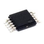
| 供应商器件封装 | 10-MSOP |
| 包装 | 管件 |
| 商标 | Analog Devices |
| 存储器类型 | OTP |
| 安装类型 | 表面贴装 |
| 安装风格 | SMD/SMT |
| 容差 | - 20 % to + 55 % |
| 封装 | Tube |
| 封装/外壳 | 10-TFSOP,10-MSOP(0.118",3.00mm 宽) |
| 封装/箱体 | MSOP-10 |
| 工作温度 | -40°C ~ 125°C |
| 工作电源电压 | 5.5 V |
| 工厂包装数量 | 50 |
| 弧刷存储器 | Volatile |
| 抽头 | 256 |
| 接口 | I²C |
| 数字接口 | I2C |
| 最大工作温度 | + 125 C |
| 最小工作温度 | - 40 C |
| 标准包装 | 50 |
| 每POT分接头 | 256 |
| 温度系数 | 35 PPM / C |
| 电压-电源 | 2.7 V ~ 5.5 V |
| 电源电压-最大 | 5.5 V |
| 电源电压-最小 | 2.7 V |
| 电源电流 | 3.5 uA |
| 电路数 | 2 |
| 电阻 | 10 kOhms |
| 电阻(Ω) | 10k |
| 系列 | AD5172 |


- 商务部:美国ITC正式对集成电路等产品启动337调查
- 曝三星4nm工艺存在良率问题 高通将骁龙8 Gen1或转产台积电
- 太阳诱电将投资9.5亿元在常州建新厂生产MLCC 预计2023年完工
- 英特尔发布欧洲新工厂建设计划 深化IDM 2.0 战略
- 台积电先进制程称霸业界 有大客户加持明年业绩稳了
- 达到5530亿美元!SIA预计今年全球半导体销售额将创下新高
- 英特尔拟将自动驾驶子公司Mobileye上市 估值或超500亿美元
- 三星加码芯片和SET,合并消费电子和移动部门,撤换高东真等 CEO
- 三星电子宣布重大人事变动 还合并消费电子和移动部门
- 海关总署:前11个月进口集成电路产品价值2.52万亿元 增长14.8%


PDF Datasheet 数据手册内容提取
256-Position, One-Time Programmable, Dual-Channel, I2C Digital Potentiometers Data Sheet AD5172/AD5173 FEATURES FUNCTIONAL BLOCK DIAGRAMS 2-channel, 256-position potentiometers A1 W1 B1 A2 W2 B2 One-time programmable (OTP) set-and-forget resistance setting provides a low cost alternative to EEMEM Unlimited adjustments prior to OTP activation OTP overwrite allows dynamic adjustments with user- defined preset VDD LFIUNSKES 1 2 End-to-end resistance: 2.5 kΩ, 10 kΩ, 50 kΩ, and 100 kΩ Compact 10-lead MSOP: 3 mm × 4.9 mm GND REGRIDSATCER 1 REGRIDSATCER 2 Fast settling time: t = 5 μs typical on power-up S Full read/write of wiper register / Power-on preset to midscale 8 SExintgrale p saucpkpaglye: 2ad.7d Vre tsos 5 d.e5c Vo de pins: AD0 and AD1 (AD5173 ) SSDCAL SERREIGALIS ITNEPRUT 04103-001 Low temperature coefficient: 35 ppm/°C Figure 1. AD5172 Functional Block Diagram Low power: IDD = 6 μA maximum W1 B1 W2 B2 Wide operating temperature: −40°C to +125°C APPLICATIONS Systems calibration VDD FUSE Electronics level setting 1 LINKS 2 Mechanical trimmers replacement in new designs RDAC RDAC Permanent factory PCB setting GND REGISTER 1 REGISTER 2 Transducer adjustment of pressure, temperature, position, chemical, and optical sensors AD0 ADDRESS RF amplifier biasing AD1 DECODE /8 Automotive electronics adjustment Gain control and offset adjustment SSDCAL SERREIGALIS ITNEPRUT 04103-002 Figure 2. AD5173 Functional Block Diagram GENERAL DESCRIPTION The AD5172/AD5173 are dual-channel, 256-position, one-time before permanently setting the resistance value. During OTP programmable (OTP) digital potentiometers1 that employ fuse activation, a permanent blow fuse command freezes the wiper link technology to achieve memory retention of resistance position (analogous to placing epoxy on a mechanical trimmer). settings. OTP is a cost-effective alternative to EEMEM for users Unlike traditional OTP digital potentiometers, the AD5172/ who do not need to program the digital potentiometer setting AD5173 have a unique temporary OTP overwrite feature that in memory more than once. These devices perform the same allows for new adjustments even after a fuse is blown. However, electronic adjustment function as mechanical potentiometers or the OTP setting is restored during subsequent power-up condi- variable resistors but with enhanced resolution, solid-state reliabil- tions. This allows users to treat these digital potentiometers as ity, and superior low temperature coefficient performance. volatile potentiometers with a programmable preset. The AD5172/AD5173 are programmed using a 2-wire, I2C®- compatible digital interface. Unlimited adjustments are allowed 1 The terms digital potentiometer, VR, and RDAC are used interchangeably. Rev. I Document Feedback Information furnished by Analog Devices is believed to be accurate and reliable. However, no responsibility is assumed by Analog Devices for its use, nor for any infringements of patents or other One Technology Way, P.O. Box 9106, Norwood, MA 02062-9106, U.S.A. rights of third parties that may result from its use. Specifications subject to change without notice. No license is granted by implication or otherwise under any patent or patent rights of Analog Devices. Tel: 781.329.4700 ©2003–2013 Analog Devices, Inc. All rights reserved. Trademarks and registered trademarks are the property of their respective owners. Technical Support www.analog.com
AD5172/AD5173 Data Sheet TABLE OF CONTENTS Features .............................................................................................. 1 Programming the Variable Resistor and Voltage ................... 16 Applications ....................................................................................... 1 Programming the Potentiometer Divider ............................... 17 Functional Block Diagrams ............................................................. 1 ESD Protection ........................................................................... 18 General Description ......................................................................... 1 Terminal Voltage Operating Range ......................................... 18 Revision History ............................................................................... 3 Power-Up Sequence ................................................................... 18 Specifications ..................................................................................... 4 Power Supply Considerations ................................................... 18 Electrical Characteristics: 2.5 kΩ ............................................... 4 Layout Considerations ............................................................... 19 Electrical Characteristics: 10 kΩ, 50 kΩ, and 100 kΩ ............. 5 I2C Interface .................................................................................... 20 Timing Characteristics ................................................................ 7 Write Mode ................................................................................. 20 Absolute Maximum Ratings ............................................................ 8 Read Mode .................................................................................. 20 ESD Caution .................................................................................. 8 I2C Controller Programming .................................................... 21 Pin Configurations and Function Descriptions ........................... 9 I2C-Compatible, 2-Wire Serial Bus .......................................... 22 Typical Performance Characteristics ........................................... 10 Level Shifting for Different Voltage Operation ...................... 23 Test Circuits ..................................................................................... 15 Outline Dimensions ....................................................................... 24 Theory of Operation ...................................................................... 16 Ordering Guide .......................................................................... 25 One-Time Programming (OTP) .............................................. 16 Rev. I | Page 2 of 28
Data Sheet AD5172/AD5173 REVISION HISTORY 8/13—Rev. H to Rev. I 6/06—Rev. C to Rev. D Changed V , V , V to GND and Digital Inputs and Output Changes to Features .......................................................................... 1 A B W Voltage to GND Rating to −0.3 V to +7 V or VDD + 0.3 V Changes to One-Time Programming (OTP) Section ................ 15 (whichever is less); Table 4 ............................................................... 7 Changes to Figure 44 and Figure 45 ............................................. 17 Changes to Ordering Guide ........................................................... 25 Changes to Power Supply Considerations Section ..................... 18 Changes to Figure 46 and Figure 47 ............................................. 18 4/09—Rev. G to Rev. H Changes to Device Programming Software Section................... 19 Changes to DC Characteristics—Rheostat Mode Parameter and Updated Outline Dimensions........................................................ 24 to DC Characteristics—Potentiometer Divider Mode Parameter, 6/05—Rev. B to Rev. C Table 1 ................................................................................................. 3 Added Footnote 8, Footnote 9, and Footnote 10 to Table 1 ........ 3 12/08—Rev. F to Rev. G Added Footnote 8 to Table 2 ............................................................ 5 Changes to OTP Supply Voltage Parameter, Table 1 .................... 3 Changes to Table 5 and Table 6 ....................................................... 9 Changes to OTP Supply Voltage Parameter, Table 2 .................... 5 Changes to Power Supply Considerations Section ..................... 17 Changes to Table 5 and Table 6 ....................................................... 8 Changes to I2C-Compatible 2-Wire Serial Bus Section ............. 23 Changes to One-Time Programming (OTP) Section ................ 15 Added Level Shifting for Different Voltage Operation Section ....... 24 Changes to Power Supply Considerations Section, Figure 46, Updated Outline Dimensions........................................................ 25 and Figure 46 Caption .................................................................... 17 Changes to Ordering Guide ........................................................... 25 Changes to Ordering Guide ........................................................... 23 10/04—Rev. A to Rev. B 7/08—Rev. E to Rev. F Updated Format ................................................................ Universal Changes to Power Supplies Parameter in Table 1 and Table 2 .... 3 Changes to Specifications................................................................. 3 Updated Fuse Blow Condition to 400 ms Throughout ................ 5 Changes to One-Time Programming (OTP) Section ................ 13 1/08—Rev. D to Rev. E Changes to Power Supply Considerations Section ..................... 15 Changes to Figure 44 and Figure 45 ............................................. 15 Changes to Features .......................................................................... 1 Changes to Figure 46 and Figure 47 ............................................. 16 Changes to General Description ..................................................... 1 Changes to OTP Supply Voltage and OTP Supply Current in 11/03—Rev. 0 to Rev. A Table 1 ................................................................................................. 3 Changes to Electrical Characteristics—2.5 kΩ ............................. 3 Changes to OTP Supply Voltage and OTP Supply Current in 11/03—Revision 0: Initial Version Table 2 ................................................................................................. 5 Added OTP Program Time in Table 3............................................ 6 Changes to Table 4 ............................................................................ 7 Changes to Table 5 and Table 6 ....................................................... 8 Inserted Figure 30............................................................................ 13 Replaced One-Time Programming (OTP) Section .................... 15 Replaced Power Supply Considerations Section ......................... 17 Deleted Device Programming Software Section ......................... 20 Replaced I2C-Compatible, 2-Wire Serial Bus Section ................ 21 Changes to Ordering Guide ........................................................... 23 Rev. I | Page 3 of 28
AD5172/AD5173 Data Sheet SPECIFICATIONS ELECTRICAL CHARACTERISTICS: 2.5 kΩ V = 5 V ± 10%, or 3 V ± 10%; V = V ; V = 0 V; −40°C < T < +125°C; unless otherwise noted. DD A DD B A Table 1. Parameter Symbol Conditions Min Typ1 Max Unit DC CHARACTERISTICS—RHEOSTAT MODE Resistor Differential Nonlinearity2 R-DNL R , V = no connect −2 ±0.1 +2 LSB WB A Resistor Integral Nonlinearity2 R-INL R , V = no connect −14 ±2 +14 LSB WB A Nominal Resistor Tolerance3 ∆R T = 25°C −20 +55 % AB A Resistance Temperature Coefficient (∆R /R )/∆T 35 ppm/°C AB AB Wiper Resistance R Code = 0x00, V = 5 V 160 200 Ω WB DD DC CHARACTERISTICS—POTENTIOMETER DIVIDER MODE4 Differential Nonlinearity5 DNL −1.5 ±0.1 +1.5 LSB Integral Nonlinearity5 INL −2 ±0.6 +2 LSB Voltage Divider Temperature Coefficient (ΔV /V )/ΔT Code = 0x80 15 ppm/°C W W Full-Scale Error V Code = 0xFF −14 −5.5 0 LSB WFSE Zero-Scale Error V Code = 0x00 0 4.5 12 LSB WZSE RESISTOR TERMINALS Voltage Range6 V , V , V GND V V A B W DD Capacitance A, B7 C , C f = 1 MHz, measured to 45 pF A B GND, code = 0x80 Capacitance W7 C f = 1 MHz, measured to 60 pF W GND, code = 0x80 Shutdown Supply Current8 I V = 5.5 V 0.01 1 µA A_SD DD Common-Mode Leakage I V = V = V /2 1 nA CM A B DD DIGITAL INPUTS AND OUTPUTS SDA and SCL Input Logic High9 V V = 5 V 0.7 V V + 0.5 V IH DD DD DD Input Logic Low9 V V = 5 V −0.5 +0.3 V V IL DD DD AD0 and AD1 Input Logic High V V = 3 V 2.1 V IH DD Input Logic Low V V = 3 V 0.6 V IL DD Input Current I V = 0 V or 5 V ±1 µA IL IN Input Capacitance7 C 5 pF IL POWER SUPPLIES Power Supply Range V 2.7 5.5 V DD_RANGE OTP Supply Voltage9, 10 V T = 25°C 5.6 5.7 5.8 V DD_OTP A Supply Current I V = 5 V or V = 0 V 3.5 6 µA DD IH IL OTP Supply Current9, 11, 12 I V = 5.0 V, T = 25°C 100 mA DD_OTP DD_OTP A Power Dissipation13 P V = 5 V or V = 0 V, V = 5 V 33 µW DISS IH IL DD Power Supply Sensitivity PSS V = 5 V ± 10%, ±0.02 ±0.08 %/% DD code = midscale DYNAMIC CHARACTERISTICS14 Bandwidth, −3 dB BW Code = 0x80 4.8 MHz Total Harmonic Distortion THD V = 1 V rms, V = 0 V, 0.1 % W A B f = 1 kHz Rev. I | Page 4 of 28
Data Sheet AD5172/AD5173 Parameter Symbol Conditions Min Typ1 Max Unit V Settling Time t V = 5 V, V = 0 V, ±1 LSB 1 µs W S A B error band Resistor Noise Voltage Density e R = 1.25 kΩ, R = 0 Ω 3.2 nV/√Hz N_WB WB S 1 Typical specifications represent average readings at 25°C and VDD = 5 V. 2 Resistor position nonlinearity error, R-INL, is the deviation from an ideal value measured between the maximum resistance and the minimum resistance wiper positions. R-DNL measures the relative step change from the ideal between successive tap positions. Parts are guaranteed monotonic. 3 VA = VDD, VB = 0 V, wiper (VW) = no connect. 4 Specifications apply to all VRs. 5 INL and DNL are measured at VW with the RDAC configured as a potentiometer divider similar to a voltage output DAC. VA = VDD and VB = 0 V. DNL specification limits of ±1 LSB maximum are guaranteed monotonic operating conditions. 6 Resistor Terminal A, Resistor Terminal B, and Resistor Terminal W have no limitations on polarity with respect to each other. 7 Guaranteed by design, but not subject to production test. 8 Measured at Terminal A. Terminal A is open circuited in shutdown mode. 9 The minimum voltage requirement on the VIH is 0.7 V × VDD. For example, VIH minimum = 3.5 V when VDD = 5 V. It is typical for the SCL and SDA resistors to be pulled up to VDD. However, care must be taken to ensure that the minimum VIH is met when the SCL and SDA are driven directly from a low voltage logic controller without pull-up resistors. 10 Different from the operating power supply; the power supply for OTP is used one time only. 11 Different from the operating current; the supply current for OTP lasts approximately 400 ms for one time only. 12 See Figure 30 for an energy plot during an OTP program. 13 PDISS is calculated from (IDD × VDD). CMOS logic level inputs result in minimum power dissipation. 14 All dynamic characteristics use VDD = 5 V. ELECTRICAL CHARACTERISTICS: 10 kΩ, 50 kΩ, AND 100 kΩ V = 5 V ± 10% or 3 V ± 10%; V = V ; V = 0 V; −40°C < T < +125°C; unless otherwise noted. DD A DD B A Table 2. Parameter Symbol Conditions Min Typ1 Max Unit DC CHARACTERISTICS—RHEOSTAT MODE Resistor Differential Nonlinearity2 R-DNL R , V = no connect −1 ±0.1 +1 LSB WB A Resistor Integral Nonlinearity2 R-INL R , V = no connect −2.5 ±0.25 +2.5 LSB WB A Nominal Resistor Tolerance3 ΔR T = 25°C −20 +20 % AB A Resistance Temperature Coefficient (ΔR /R )/ΔT 35 ppm/°C AB AB Wiper Resistance R Code = 0x00, V = 5 V 160 200 Ω WB DD DC CHARACTERISTICS—POTENTIOMETER DIVIDER MODE4 Differential Nonlinearity5 DNL −1 ±0.1 +1 LSB Integral Nonlinearity5 INL −1 ±0.3 +1 LSB Voltage Divider Temperature Coefficient (ΔV /V )/ΔT Code = 0x80 15 ppm/°C W W Full-Scale Error V Code = 0xFF −2.5 −1 0 LSB WFSE Zero-Scale Error V Code = 0x00 0 1 2.5 LSB WZSE RESISTOR TERMINALS Voltage Range6 V , V , V GND V V A B W DD Capacitance A, B7 C , C f = 1 MHz, measured to 45 pF A B GND, code = 0x80 Capacitance W7 C f = 1 MHz, measured to 60 pF W GND, code = 0x80 Shutdown Supply Current8 I V = 5.5 V 0.01 1 µA A_SD DD Common-Mode Leakage I V = V = V /2 1 nA CM A B DD DIGITAL INPUTS AND OUTPUTS SDA and SCL Input Logic High9 V V = 5 V 0.7 V V + 0.5 V IH DD DD DD Input Logic Low9 V V = 5 V −0.5 +0.3 V V IL DD DD AD0 and AD1 Input Logic High V V = 3 V 2.1 V IH DD Input Logic Low V V = 3 V 0.6 V IL DD Input Current I V = 0 V or 5 V ±1 µA IL IN Input Capacitance7 C 5 pF IL Rev. I | Page 5 of 28
AD5172/AD5173 Data Sheet Parameter Symbol Conditions Min Typ1 Max Unit POWER SUPPLIES Power Supply Range V 2.7 5.5 V DD_RANGE OTP Supply Voltage9, 10 V T = 25°C 5.6 5.7 5.8 V DD_OTP A Supply Current I V = 5 V or V = 0 V 3.5 6 µA DD IH IL OTP Supply Current9, 11, 12 I V = 5.0 V, T = 25°C 100 mA DD_OTP DD_OTP A Power Dissipation13 P V = 5 V or V = 0 V, 33 µW DISS IH IL V = 5 V DD Power Supply Sensitivity PSS V = 5 V ± 10%, ±0.02 ±0.08 %/% DD code = midscale DYNAMIC CHARACTERISTICS14 Bandwidth, −3 dB BW R = 10 kΩ, code = 0x80 600 kHz AB R = 50 kΩ, code = 0x80 100 kHz AB R = 100 kΩ, code = 0x80 40 kHz AB Total Harmonic Distortion THD V = 1 V rms, V = 0 V, 0.1 % W A B f = 1 kHz, R = 10 kΩ AB V Settling Time t V = 5 V, V = 0 V, ±1 LSB 2 µs W S A B error band Resistor Noise Voltage Density e R = 5 kΩ, R = 0 Ω 9 nV/√Hz N_WB WB S 1 Typical specifications represent average readings at 25°C and VDD = 5 V. 2 Resistor position nonlinearity error, R-INL, is the deviation from an ideal value measured between the maximum resistance and the minimum resistance wiper positions. R-DNL measures the relative step change from the ideal between successive tap positions. Parts are guaranteed monotonic. 3 VA = VDD, VB = 0 V, wiper (VW) = no connect. 4 Specifications apply to all VRs. 5 INL and DNL are measured at VW with the RDAC configured as a potentiometer divider similar to a voltage output DAC. VA = VDD and VB = 0 V. DNL specification limits of ±1 LSB maximum are guaranteed monotonic operating conditions. 6 Resistor Terminal A, Resistor Terminal B, and Resistor Terminal W have no limitations on polarity with respect to each other. 7 Guaranteed by design, but not subject to production test. 8 Measured at Terminal A. Terminal A is open circuited in shutdown mode. 9 The minimum voltage requirement on the VIH is 0.7 V × VDD. For example, VIH minimum = 3.5 V when VDD = 5 V. It is typical for the SCL and SDA resistors to be pulled up to VDD. However, care must be taken to ensure that the minimum VIH is met when the SCL and SDA are driven directly from a low voltage logic controller without pull-up resistors. 10 Different from the operating power supply; the power supply for OTP is used one time only. 11 Different from the operating current; the supply current for OTP lasts approximately 400 ms for one time only. 12 See Figure 30 for an energy plot during an OTP program. 13 PDISS is calculated from (IDD × VDD). CMOS logic level inputs result in minimum power dissipation. 14 All dynamic characteristics use VDD = 5 V. Rev. I | Page 6 of 28
Data Sheet AD5172/AD5173 TIMING CHARACTERISTICS V = 5 V ± 10%, or 3 V ± 10%; V = V ; V = 0 V; −40°C < T < +125°C; unless otherwise noted. DD A DD B A Table 3. Parameter Symbol Conditions Min Typ Max Unit I2C INTERFACE TIMING CHARACTERISTICS1 SCL Clock Frequency f 400 kHz SCL Bus-Free Time Between Stop and Start, t t 1.3 μs BUF 1 Hold Time (Repeated Start), t t After this period, the first clock 0.6 μs HD;STA 2 pulse is generated. Low Period of SCL Clock, t t 1.3 μs LOW 3 High Period of SCL Clock, t t 0.6 μs HIGH 4 Setup Time for Repeated Start Condition, t t 0.6 μs SU;STA 5 Data Hold Time, t 2 t 0.9 μs HD;DAT 6 Data Setup Time, t t 100 ns SU;DAT 7 Fall Time of Both SDA and SCL Signals, t t 300 ns F 8 Rise Time of Both SDA and SCL Signals, t t 300 ns R 9 Setup Time for Stop Condition, t t 0.6 μs SU;STO 10 OTP Program Time t 400 ms 11 1 See the timing diagrams for the locations of measured values (that is, see Figure 3 and Figure 48 to Figure 51). 2 The maximum tHD;DAT has to be met only if the device does not stretch the low period (tLOW) of the SCL signal. Timing Diagram t8 t6 t9 t2 SCL t2 t3 t4 t7 t5 t10 t8 t9 SDA P t1 S S P 04103-0-039 Figure 3. I2C Interface Detailed Timing Diagram Rev. I | Page 7 of 28
AD5172/AD5173 Data Sheet ABSOLUTE MAXIMUM RATINGS T = 25°C, unless otherwise noted. A Table 4. Stresses above those listed under Absolute Maximum Ratings Parameter Rating may cause permanent damage to the device. This is a stress V to GND −0.3 V to +7 V DD rating only; functional operation of the device at these or any V , V, V to GND −0.3 V to +7 V or A B W V + 0.3 V other conditions above those indicated in the operational DD (whichever is less) section of this specification is not implied. Exposure to absolute Terminal Current, Ax to Bx, Ax to Wx, Bx to Wx1 maximum rating conditions for extended periods may affect Pulsed ±20 mA device reliability. Continuous ±5 mA Digital Inputs and Output Voltage to GND −0.3 V to +7 V or V + 0.3 V ESD CAUTION DD (whichever is less) Operating Temperature Range −40°C to +125°C Maximum Junction Temperature (T ) 150°C JMAX Storage Temperature Range −65°C to +150°C Reflow Soldering Peak Temperature 260°C Time at Peak Temperature 20 sec to 40 sec Thermal Resistance2 θ for 10-Lead MSOP 200°C/W JA 1 The maximum terminal current is bound by the maximum current handling of the switches, the maximum power dissipation of the package, and the maximum applied voltage across any two of the A, B, and W terminals at a given resistance. 2 The package power dissipation is (TJMAX − TA)/θJA. Rev. I | Page 8 of 28
Data Sheet AD5172/AD5173 PIN CONFIGURATIONS AND FUNCTION DESCRIPTIONS B1 1 10 W1 B1 1 10 W1 A1 2 AD5172 9 B2 AD0 2 AD5173 9 B2 W2 3 TOP VIEW 8 A2 W2 3 TOP VIEW 8 AD1 GVNDDD 54 (Not to Scale) 76 SSDCAL 04103-045 GVNDDD 54 (Not to Scale) 76 SSDCLA 04103-046 Figure 4. AD5172 Pin Configuration Figure 5. AD5173 Pin Configuration Table 5. AD5172 Pin Function Descriptions Table 6. AD5173 Pin Function Descriptions Pin Pin No. Mnemonic Description No. Mnemonic Description 1 B1 B1 Terminal. GND ≤ V ≤ V . 1 B1 B1 Terminal. GND ≤ V ≤ V . B1 DD B1 DD 2 A1 A1 Terminal. GND ≤ V ≤ V . 2 AD0 Programmable Address Bit 0 for Multiple A1 DD 3 W2 W2 Terminal. GND ≤ V ≤ V . Package Decoding. W2 DD 4 GND Digital Ground. 3 W2 W2 Terminal. GND ≤ VW2 ≤ VDD. 5 V Positive Power Supply. Specified for 4 GND Digital Ground. DD operation from 2.7 V to 5.5 V. For OTP 5 V Positive Power Supply. Specified for DD programming, V needs to be a minimum operation from 2.7 V to 5.5 V. For OTP DD of 5.6 V but no more than 5.8 V and to be programming, V needs to be a minimum DD capable of driving 100 mA. of 5.6 V but no more than 5.8 V and to be 6 SCL Serial Clock Input. Positive-edge triggered. capable of driving 100 mA. Requires a pull-up resistor. If this pin is driven 6 SCL Serial Clock Input. Positive-edge triggered. directly from a logic controller without a Requires a pull-up resistor. If this pin is driven pull-up resistor, ensure that the V minimum directly from a logic controller without a IH is 0.7 V × VDD. pull-up resistor, ensure that the VIH minimum 7 SDA Serial Data Input/Output. Requires a pull-up is 0.7 V × VDD. resistor. If this pin is driven directly from a 7 SDA Serial Data Input/Output. Requires a pull-up logic controller without a pull-up resistor, resistor. If this pin is driven directly from a ensure that the V minimum is 0.7 V × V . logic controller without a pull-up resistor, IH DD 8 A2 A2 Terminal. GND ≤ VA2 ≤ VDD. ensure that the VIH minimum is 0.7 V × VDD. 9 B2 B2 Terminal. GND ≤ V ≤ V . 8 AD1 Programmable Address Bit 1 for Multiple B2 DD Package Decoding. 10 W1 W1 Terminal. GND ≤ V ≤ V . W1 DD 9 B2 B2 Terminal. GND ≤ V ≤ V . B2 DD 10 W1 W1 Terminal. GND ≤ V ≤ V . W1 DD Rev. I | Page 9 of 28
AD5172/AD5173 Data Sheet TYPICAL PERFORMANCE CHARACTERISTICS 2.0 0.5 TA = 25°C RAB = 10kΩ 1.5 RAB = 10kΩ 0.4 B) S 0.3 LSB) 1.0 VDD = 2.7V NL (L 0.2 E INL ( 0.5 ODE D 0.1 VDD = 2.7V; TA = –40°C, +25°C, +85°C, +125°C D M MO 0 ER 0 TAT –0.5 VDD = 5.5V MET –0.1 S O RHEO –1.0 OTENTI ––00..32 P ––21..05 04103-003 ––00..54 04103-006 0 32 64 96 128 160 192 224 256 0 32 64 96 128 160 192 224 256 CODE (DECIMAL) CODE (DECIMAL) Figure 6. R-INL vs. Code vs. Supply Voltages Figure 9. DNL vs. Code vs. Temperature 0.5 1.0 TA = 25°C TA = 25°C 0.4 RAB = 10kΩ 0.8 RAB = 10kΩ B) B) 0.3 LS 0.6 ODE DNL (LS 00..012 VDD = 2.7V R MODE INL ( 00..024 VDD = 5.5V M E AT –0.1 MET –0.2 VDD = 2.7V EOST –0.2 NTIO –0.4 H E R –0.3 VDD = 5.5V OT –0.6 P ––00..54 04103-004 ––10..08 04103-007 0 32 64 96 128 160 192 224 256 0 32 64 96 128 160 192 224 256 CODE (DECIMAL) CODE (DECIMAL) Figure 7. R-DNL vs. Code vs. Supply Voltages Figure 10. INL vs. Code vs. Supply Voltages 0.5 0.5 RAB = 10kΩ TA = 25°C 0.4 0.4 RAB = 10kΩ B) B) E INL (LS 00..23 TVAD D= =– 450.5°VC, +25°C, +85°C, +125°C E DNL (LS 00..23 MOD 0.1 MOD 0.1 VDD = 2.7V R 0 R 0 E E MET –0.1 MET –0.1 ENTIO –0.2 TVAD D= =– 420.7°VC, +25°C, +85°C, +125°C ENTIO –0.2 VDD = 5.5V OT –0.3 OT –0.3 P P ––00..54 04103-005 ––00..54 04103-008 0 32 64 96 128 160 192 224 256 0 32 64 96 128 160 192 224 256 CODE (DECIMAL) CODE (DECIMAL) Figure 8. INL vs. Code vs. Temperature Figure 11. DNL vs. Code vs. Supply Voltages Rev. I | Page 10 of 28
Data Sheet AD5172/AD5173 2.0 4.50 RAB = 10kΩ RAB = 10kΩ 1.5 VDD = 2.7V TA = –40°C, +25°C, +85°C, +125°C B) 3.75 B) 1.0 LS LS R ( DE INL ( 0.5 E ERRO 3.00 MO 0 AL 2.25 VDD = 2.7V, VA = 2.7V OSTAT –0.5 TVAD D= =– 450.5°VC, +25°C, +85°C, +125°C ERO-SC 1.50 E Z RH –1.0 E, VDD = 5.5V, VA = 5.0V S Z 0.75 ––21..05 04103-009 0 04103-012 0 32 64 96 128 160 192 224 256 –40 –25 –10 5 20 35 50 65 80 95 110 125 CODE (DECIMAL) TEMPERATURE (°C) Figure 12. R-INL vs. Code vs. Temperature Figure 15. Zero-Scale Error vs. Temperature 0.5 10 RAB = 10kΩ 0.4 E DNL (LSB) 000...123 VDD = 2.7V, 5.5V; TA = –40°C, +25°C, +85°C, +125°C RRENT(µA) VDD = 5V D U O 0 C 1 M Y TAT –0.1 PPL VDD = 3V S U RHEO ––00..32 I, SDD ––00..54 04103-010 0.1 04103-013 0 32 64 96 128 160 192 224 256 –40 –7 26 59 92 125 CODE (DECIMAL) TEMPERATURE (°C) Figure 13. R-DNL vs. Code vs. Temperature Figure 16. Supply Current vs. Temperature 2.0 120 RAB = 10kΩ RAB = 10kΩ 1.5 C) 100 SCALE ERROR (LSB) 01..050 VDD = 5.5V, VA = 5.0V ODE TEMPCO (ppm/° 468000 TVAD D= =– 420.7°VC TO +85°C, –40°C TO +125°C ULL- –0.5 AT M TVAD D= =– 450.5°VC TO +85°C, –40°C TO +125°C E, F –1.0 VDD = 2.7V, VA = 2.7V OST 20 FS HE ––21..05 04103-011 R –200 04103-014 –40 –25 –10 5 20 35 50 65 80 95 110 125 0 32 64 96 128 160 192 224 256 TEMPERATURE (°C) CODE (DECIMAL) Figure 14. Full-Scale Error vs. Temperature Figure 17. Rheostat Mode Tempco ΔRWB/ΔT vs. Code Rev. I | Page 11 of 28
AD5172/AD5173 Data Sheet 50 0 m/°C) 40 RAB = 10kΩ –6 0x80 pp –12 0x40 CO ( 30 –18 0x20 ODE TEMP 1200 TVAD D= =– 420.7°VC TO +85°C, –40°C TO +125°C N (dB) ––3204 00xx1008 ER M 0 GAI –36 0x04 ET 0x02 M –42 ENTIO –10 TVAD D= =– 450.5°VC TO +85°C, –40°C TO +125°C –48 0x01 POT ––3200 04103-047 ––6504 04103-050 0 32 64 96 128 160 192 224 256 1k 10k 100k 1M CODE (DECIMAL) FREQUENCY (Hz) Figure 18. AD5172 Potentiometer Mode Tempco ΔVWB/ΔT vs. Code Figure 21. Gain vs. Frequency vs. Code, RAB = 50 kΩ 0 0 0x80 0x80 –6 –6 0x40 0x40 –12 –12 0x20 0x20 –18 –18 0x10 0x10 B) –24 0x08 B) –24 N (d –30 0x04 N (d –30 0x08 AI AI G –36 G –36 0x04 0x02 0x01 0x02 –42 –42 0x01 –48 –48 ––6504 04103-048 ––6504 04103-051 10k 100k 1M 10M 1k 10k 100k 1M FREQUENCY (Hz) FREQUENCY (Hz) Figure 19. Gain vs. Frequency vs. Code, RAB = 2.5 kΩ Figure 22. Gain vs. Frequency vs. Code, RAB = 100 kΩ 0 0 0x80 –6 –6 –12 0x40 –12 100kΩ –18 0x20 –18 60kHz 50kΩ 0x10 120kHz B) –24 B) –24 10kΩ N (d –30 0x08 N (d –30 570kHz AI 0x04 AI 2.5kΩ G –36 0x02 G –36 2.2MHz 0x01 –42 –42 –48 –48 ––6504 04103-049 ––6504 04103-052 1k 10k 100k 1M 1k 10k 100k 1M 10M FREQUENCY (Hz) FREQUENCY (Hz) Figure 20. Gain vs. Frequency vs. Code, RAB = 10 kΩ Figure 23. −3 dB Bandwidth at Code = 0x80 Rev. I | Page 12 of 28
Data Sheet AD5172/AD5173 10 TA = 25°C A) m T ( 1 N RE VDD = 5.5V R CU VW2 Y L P P SU 0.1 , D ID VDD = 2.7V 0.010 0.5 1.0 1.5 2.0 2.5 3.0 3.5 4.0 4.5 5.004103-057 VW1 04103-056 DIGITAL INPUT VOLTAGE (V) Figure 24. Supply Current vs. Digital Input Voltage Figure 27. Analog Crosstalk VW VW SCL 04103-053 04103-058 Figure 25. Digital Feedthrough Figure 28. Midscale Glitch, Code 0x80 to Code 0x7F VW2 VW VW1 SCL 04103-054 04103-055 Figure 26. Digital Crosstalk Figure 29. Large-Signal Settling Time Rev. I | Page 13 of 28
AD5172/AD5173 Data Sheet T CHANNEL 1 MAXIMUM: 103mA CHANNEL 1 MINIMUM: –1.98mA 1 04103-062 CH1 20.0mA M 200ns A CH1 32.4mA T 588.000ns Figure 30. OTP Program Energy for Single Fuse Rev. I | Page 14 of 28
Data Sheet AD5172/AD5173 TEST CIRCUITS Figure 31 to Figure 38 illustrate the test circuits that define the test conditions used in the product specification tables (see Table 1 and Table 2). A DUT V+= VDD DUT +5V V+ A W 1LSB = V+/2N OFFSET VIN W AD8610 VOUT B VMS 04103-015 GND 2.5V B –5V 04103-019 Figure 31. Potentiometer Divider Nonlinearity Error (INL, DNL) Figure 35. Test Circuit for Gain vs. Frequency NC 0.1V DUT DUT RSW= ISW IW CODE = 0x00 A W W B ISW 0.1V VMS B NC = NO CONNECT 04103-016 GND TO VDD 04103-020 Figure 32. Resistor Position Nonlinearity Error (Rheostat Operation: R-INL, R-DNL) Figure 36. Incremental On Resistance NC DUT VDD A ICM DUT W VMS2 A W VW IW= VDD/RNOMINAL GND B VCM B VMS1 RW= [VMS1– VMS2]/IW 04103-017 NC = NO CONNNCECT 04103-021 Figure 33. Wiper Resistance Figure 37. Common-Mode Leakage Current A1 A2 VDD RDAC1 RDAC2 VA W1 W2 V+ VDD ADUWT PPV+SS SR= R(V% D(dD/%B±)) 1==0 2%Δ0V lMoSg%(ΔΔVVDMDS) VIN NC B1 VSS B2 VOUT ΔVDD% B VMS 04103-018 NCCTA = =N 2O0 CloOgN[VNOEUCTT/VIN] 04103-022 Figure 34. Power Supply Sensitivity (PSS, PSSR) Figure 38. Analog Crosstalk Rev. I | Page 15 of 28
AD5172/AD5173 Data Sheet THEORY OF OPERATION A SCL I2C INTERFACE DAC MUX DECODER SDA REG W B COMPARATOR FUSES FUSE EN REG ONE-TIME PROGRAM/TEST CONTROL BLOCK 04103-026 Figure 39. Detailed Functional Block Diagram The AD5172/AD5173 are 256-position, digitally controlled Table 7. Validation Status variable resistors (VRs) that employ fuse link technology to E1 E0 Status achieve memory retention of the resistance setting. 0 0 Ready for programming. An internal power-on preset places the wiper at midscale 1 0 Fatal error. Some fuses are not blown. Do not retry. during power-on. If the OTP function is activated, the device Discard this unit. powers up at the user-defined permanent setting. 1 1 Successful. No further programming is possible. ONE-TIME PROGRAMMING (OTP) PROGRAMMING THE VARIABLE RESISTOR AND Prior to OTP activation, the AD5172/AD5173 presets to midscale VOLTAGE during initial power-on. After the wiper is set to the desired Rheostat Operation position, the resistance can be permanently set by programming the T bit high, with the proper coding (see Table 8 and Table 9), The nominal resistance of the RDAC between Terminal A and and one-time VDD_OTP. The fuse link technology of the AD517x Terminal B is available in 2.5 kΩ, 10 kΩ, 50 kΩ, and 100 kΩ. family of digital potentiometers requires VDD_OTP to be between The nominal resistance (RAB) of the VR has 256 contact points 5.6 V and 5.8 V to blow the fuses to achieve a given nonvolatile accessed by the wiper terminal and the B terminal contact. The setting. However, during operation, VDD can be 2.7 V to 5.5 V. As a 8-bit data in the RDAC latch is decoded to select one of the result, an external supply is required for one-time programming. 256 possible settings. The user is allowed only one attempt to blow the fuses. If the user fails to blow the fuses during this attempt, the structure of the A A A fuses can change such that they may never be blown, regardless W W W othf et hPeo ewneerr Sguyp applpyl iCeodn dsuidrienragt siounbss esqeucteinotn e. vents. For details, see B B B 04103-027 The device control circuit has two validation bits, E1 and E0, Figure 40. Rheostat Mode Configuration that can be read back to check the programming status (see Assuming a 10 kΩ part is used, the first connection of the wiper Table 7). Users should always read back the validation bits to starts at the B terminal for Data 0x00. Because there is a 50 Ω ensure that the fuses are properly blown. After the fuses are wiper contact resistance, such a connection yields a minimum blown, all fuse latches are enabled upon subsequent power-on; of 100 Ω (2 × 50 Ω) resistance between Terminal W and Ter- therefore, the output corresponds to the stored setting. Figure 39 minal B. The second connection is the first tap point, which shows a detailed functional block diagram. corresponds to 139 Ω (R = R /256 + 2 × R = 39 Ω + 2 × WB AB W 50 Ω) for Data 0x01. The third connection is the next tap point, representing 178 Ω (2 × 39 Ω + 2 × 50 Ω) for Data 0x02, and so on. Each LSB data value increase moves the wiper up the resistor ladder until the last tap point is reached at 10,100 Ω (R + 2 × R ). AB W Rev. I | Page 16 of 28
Data Sheet AD5172/AD5173 When R is 10 kΩ and the B terminal is open circuited, the A AB RS output resistance, RWA, is set according to the RDAC latch codes, as listed in Table 9. D7 RS Table 9. Codes and Corresponding R Resistance D6 WA D5 D4 D (Dec) RWA (Ω) Output State D3 RS D2 255 139 Full scale D1 D0 W 128 5060 Midscale 1 9961 1 LSB 0 10,060 Zero scale Typical device-to-device matching is process-lot dependent RDAC RS and can vary up to ±30%. Because the resistance element is LATCH DECAONDDER B processed using thin-film technology, the change in RAB with 04103-028 PteRmOpeGraRtuAreM haMs aIN veGry T loHwE t ePmOpTerEatNurTeI cOoeMffiEcTieEntR o fD 3I5V pIpDmE/R°C . Figure 41. AD5172/AD5173 Equivalent RDAC Circuit Voltage Output Operation The general equation that determines the digitally programmed The digital potentiometer easily generates a voltage divider at output resistance between W and B is wiper to B and at wiper to A, proportional to the input voltage D R (D) R 2R (1) at A to B. Unlike the polarity of VDD to GND, which must be WB 128 AB W positive, voltage across A to B, W to A, and W to B can be at where: either polarity. D is the decimal equivalent of the binary code loaded in the VI 8-bit RDAC register. A R is the end-to-end resistance. AB W R is the wiper resistance contributed by the on resistance of VO W tInh es uinmtemrnarayl , siwf RitAcBh i.s 10 kΩ and the A terminal is open circuited, B 04103-029 Figure 42. Potentiometer Mode Configuration the output resistance, R , is set according to the RDAC latch WB codes, as listed in Table 8. If ignoring the effect of the wiper resistance for approximation, connecting the A terminal to 5 V and the B terminal to ground Table 8. Codes and Corresponding RWB Resistance produces an output voltage at the wiper to B, starting at 0 V up D (Dec) RWB (Ω) Output State to 1 LSB less than 5 V. Each LSB of voltage is equal to the vol- 255 9961 Full scale (RAB – 1 LSB + RW) tage applied across Terminal A and Terminal B divided by the 128 5060 Midscale 256 positions of the potentiometer divider. The general equation 1 139 1 LSB defining the output voltage at V with respect to ground for any W 0 100 Zero scale (wiper contact resistance) valid input voltage applied to Terminal A and Terminal B is D 256D Note that in the zero-scale condition, a finite wiper resistance of V (D) V V (3) W 256 A 256 B 100 Ω is present. Care should be taken to limit the current flow A more accurate calculation, which includes the effect of wiper between W and B in this state to a maximum pulse current of resistance, V , is no more than 20 mA. Otherwise, degradation or possible destruc- W tion of the internal switch contact may occur. R (D) R (D) V (D) WB V WA V (4) Similar to the mechanical potentiometer, the resistance of the W R A R B AB AB RDAC between Wiper W and Terminal A also produces a digi- Operation of the digital potentiometer in the divider mode tally controlled complementary resistance, R . When these WA results in more accurate operation over temperature. Unlike in terminals are used, the B terminal can be opened. Setting the the rheostat mode, the output voltage is dependent mainly on resistance value for R starts at a maximum value of resistance WA the ratio of the internal resistors, R and R , not on the absolute WA WB and decreases as the data loaded in the latch increases in value. values. Therefore, the temperature drift reduces to 15 ppm/°C. The general equation for this operation is 256–D R (D) R 2R (2) WA 128 AB W Rev. I | Page 17 of 28
AD5172/AD5173 Data Sheet ESD PROTECTION rack-mount power supply) must be rated at 5.6 V to 5.8 V and must be able to provide a 100 mA transient current for 400 ms All digital inputs, SDA, SCL, AD0, and AD1, are protected with for successful one-time programming. When programming a series input resistor and parallel Zener ESD structures, as is completed, the V supply must be removed to allow shown in Figure 43 and Figure 44. DD_OTP normal operation at 2.7 V to 5.5 V; the device consumes only 340Ω LOGIC microamps of current. GND 04103-030 5.7V R1 APPLY FOR OTP ONLY Figure 43. ESD Protection of Digital Pins 10kΩ 2.7V VDD C1 C2 A, B, W P1 P2 10µF 0.1µF AD5172/ AD5173 GND 04103-031 P1 = P2 = FDV302P, NDS0610 TERMINALF igVuOre L44T. AESGD PEr oOtePctEioRn oAf TReIsNistGor RTeArmNinGalsE 04103-035 Figure 46. Isolate 5.7 V OTP Supply from 2.7 V Normal Operating Supply The AD5172/AD5173 V to GND power supply defines the DD For example, for those who operate their systems at 2.7 V, use of boundary conditions for proper 3-terminal digital potenti- the bidirectional, low threshold, P-channel MOSFETs is recom- ometer operation. Supply signals present on Terminal A, mended for the isolation of the supply. As shown in Figure 46, Terminal B, and Terminal W that exceed V or GND are DD this assumes that the 2.7 V system voltage is applied first and clamped by the internal forward-biased diodes (see Figure 45). that the P1 and P2 gates are pulled to ground, thus turning on VDD P1 and then P2. As a result, VDD of the AD5172/AD5173 approaches 2.7 V. When the AD5172/AD5173 setting is found, A the factory tester applies the V to both the V and the DD_OTP DD W MOSFET gates, thus turning P1 and P2 off. To program the AD5172/AD5173 while the 2.7 V source is protected, execute B GND 04103-032 tthhee OtesTtPer c womithmdaranwds a tth teh iVs DtiDm_OeT.P ,W anhde nth teh ese OttTinPg iosf c tohme pAlDet5ed17, 2 Figure 45. Maximum Terminal Voltages Set by VDD and GND or AD5173 is fixed permanently. POWER-UP SEQUENCE The AD5172/AD5173 achieve the OTP function by blowing internal fuses. Always apply the 5.6 V to 5.8 V one-time pro- Because the ESD protection diodes limit the voltage compliance gram voltage requirement at the first fuse programming attempt. at Terminal A, Terminal B, and Terminal W (see Figure 45), it Failure to comply with this requirement may lead to changing is important to power V /GND before applying voltage to DD the fuse structures, rendering programming inoperable. Terminal A, Terminal B, and Terminal W. Otherwise, the diode is forward-biased such that V is powered unintentionally and Care should be taken when SCL and SDA are driven from a low DD may affect the rest of the user’s circuit. The ideal power-up voltage logic controller. Users must ensure that the logic high sequence is GND, VDD, digital inputs, and then VA/VB/VW. The level is between 0.7 V × VDD and VDD + 0.5 V. relative order of powering VA, VB, VW, and the digital inputs is Poor PCB layout introduces parasitics that can affect fuse not important, as long as they are powered after VDD/GND. programming. Therefore, it is recommended to add a 1 µF to POWER SUPPLY CONSIDERATIONS 10 µF tantalum capacitor in parallel with a 1 nF ceramic capacitor as close as possible to the VDD pin. The type and value chosen for To minimize the package pin count, both the one-time pro- both capacitors are important. These capacitors work together to gramming and normal operating voltage supplies are applied to provide both fast responsiveness and large supply current handling the same V terminal of the device. The AD5172/AD5173 DD with minimum supply droop during transients. As a result, employ fuse link technology that requires 5.6 V to 5.8 V to blow these capacitors increase the OTP programming success by not the internal fuses to achieve a given setting, but normal V can DD inhibiting the proper energy needed to blow the internal fuses. be 2.7 V to 5.5 V. Such dual-voltage requirements need isolation Additionally, C1 minimizes transient disturbance and low between the supplies if V is lower than the required V . DD DD_OTP frequency ripple, whereas C2 reduces high frequency noise The fuse programming supply (either an on-board regulator or during normal operation. Rev. I | Page 18 of 28
Data Sheet AD5172/AD5173 LAYOUT CONSIDERATIONS In PCB layout, it is a good practice to employ compact, minimum VDD VDD + lead length design. The leads to the inputs should be as direct as C1 C2 10µF 0.1µF AD5172 possible with a minimum conductor length. Ground paths should have low resistance and low inductance. Note that the digital ground should also be joined remotely to GND the analog ground at one point to minimize the ground bounce. 04103-036 Figure 47. Power Supply Bypassing Rev. I | Page 19 of 28
AD5172/AD5173 Data Sheet I2C INTERFACE WRITE MODE Table 10. AD5172 Write Mode S 0 1 0 1 1 1 1 W A A0 SD T 0 OW X X X A D7 D6 D5 D4 D3 D2 D1 D0 A P Slave address byte Instruction byte Data byte Table 11. AD5173 Write Mode S 0 1 0 1 1 AD1 AD0 W A A0 SD T 0 OW X X X A D7 D6 D5 D4 D3 D2 D1 D0 A P Slave address byte Instruction byte Data byte READ MODE Table 12. AD5172 Read Mode S 0 1 0 1 1 1 1 R A D7 D6 D5 D4 D3 D2 D1 D0 A E1 E0 X X X X X X A P Slave address byte Instruction byte Data byte Table 13. AD5173 Read Mode S 0 1 0 1 1 AD1 AD0 R A D7 D6 D5 D4 D3 D2 D1 D0 A E1 E0 X X X X X X A P Slave address byte Instruction byte Data byte Table 14. SDA Bits Descriptions Bit Description S Start condition. P Stop condition. A Acknowledge. AD0, AD1 Package pin-programmable address bits. X Don’t care. W Write. R Read. A0 RDAC subaddress select bit. SD Shutdown connects wiper to B terminal and open circuits the A terminal. It does not change the contents of the wiper register. T OTP programming bit. Logic 1 programs the wiper permanently. OW Overwrites the fuse setting and programs the digital potentiometer to a different setting. Upon power-up, the digital potentiometer is preset to either midscale or fuse setting, depending on whether the fuse link was blown. D7, D6, D5, D4, D3, D2, D1, D0 Data bits. E1, E0 OTP validation bits. 00 = ready to program. 10 = fatal error. Some fuses not blown. Do not retry. Discard this unit. 11 = programmed successfully. No further adjustments are possible. Rev. I | Page 20 of 28
Data Sheet AD5172/AD5173 I2C CONTROLLER PROGRAMMING Write Bit Patterns 1 9 1 9 1 9 SCL SDA 0 1 0 1 1 1 1 R/W A0 SD T 0 OW X X X D7 D6 D5 D4 D3 D2 D1 D0 ACK BY ACK BY ACK BY AD5172 AD5172 AD5172 SMTAASRTTE RBY SLAVE FARDADMREE S1S BYTE INSTRFURCATMIOEN 2 BYTE DFARTAAM BEY T3E SMTAOSPT EBRY 04103-040 Figure 48. Writing to the RDAC Register—AD5172 1 9 1 9 1 9 SCL SDA 0 1 0 1 1 AD1 AD0 R/W A0 SD T 0 OW X X X D7 D6 D5 D4 D3 D2 D1 D0 ACK BY ACK BY ACK BY AD5173 AD5173 AD5173 SMTAASRTTE RBY SLAVE FARDADMREE S1S BYTE INSTRFURCATMIOEN 2 BYTE DFARTAAM BEY T3E SMTAOSPT EBRY 04103-041 Figure 49. Writing to the RDAC Register—AD5173 Read Bit Patterns 1 9 1 9 1 9 SCL SDA 0 1 0 1 1 1 1 R/W D7 D6 D5 D4 D3 D2 D1 D0 E1 E0 X X X X X X ACK BY ACK BY NO ACK AD5172 MASTER BY MASTER SMTAASRTTE RBY SLAVE FARDADMREE S1S BYTE INSTRFURCATMIOEN 2 BYTE DFARTAAM BEY T3E SMTAOSPT EBRY 04103-042 Figure 50. Reading Data from a Previously Selected RDAC Register in Write Mode—AD5172 1 9 1 9 1 9 SCL SDA 0 1 0 1 1 AD1 AD0 R/W D7 D6 D5 D4 D3 D2 D1 D0 E1 E0 X X X X X X ACK BY ACK BY NO ACK AD5173 MASTER BY MASTER SMTAASRTTE RBY SLAVE FARDADMREE S1S BYTE INSTRFURCATMIOEN 2 BYTE DFARTAAM BEY T3E SMTAOSPT EBRY 04103-043 Figure 51. Reading Data from a Previously Selected RDAC Register in Write Mode—AD5173 Rev. I | Page 21 of 28
AD5172/AD5173 Data Sheet I2C-COMPATIBLE, 2-WIRE SERIAL BUS After acknowledging the instruction byte, the last byte in write mode is the data byte. Data is transmitted over the serial bus in This section describes how the 2-wire, I2C-compatible serial bus sequences of nine clock pulses (eight data bits followed by an protocol operates. acknowledge bit). The transitions on the SDA line must occur The master initiates a data transfer by establishing a start during the low period of SCL and remain stable during the high condition, which is when a high-to-low transition on the SDA period of SCL (see Figure 3). line occurs while SCL is high (see Figure 48 and Figure 49). In read mode, the data byte follows immediately after the The following byte is the slave address byte, which consists of acknowledgment of the slave address byte. Data is transmitted the slave address followed by an R/W bit (this bit determines over the serial bus in sequences of nine clock pulses (a slight whether data is read from or written to the slave device). The difference from the write mode, where there are eight data bits AD5172 has a fixed slave address byte, whereas the AD5173 followed by an acknowledge bit). Similarly, transitions on the has two configurable address bits, AD0 and AD1 (see Figure 48 SDA line must occur during the low period of SCL and remain and Figure 49). stable during the high period of SCL (see Figure 50 and Figure 51). The slave whose address corresponds to the transmitted address Note that the channel of interest is the one that is previously responds by pulling the SDA line low during the ninth clock selected in write mode. If users need to read the RDAC values pulse (this is called the acknowledge bit). At this stage, all other of both channels, they must program the first channel in write devices on the bus remain idle while the selected device waits mode and then change to read mode to read the first channel for data to be written to or read from its serial register. If the value. After that, the user must return to write mode with the R/W bit is high, the master reads from the slave device. If the second channel selected and read the second channel value in R/W bit is low, the master writes to the slave device. read mode. It is not necessary for users to issue the Frame 3 In write mode, the second byte is the instruction byte. The first data byte in write mode for subsequent readback operations. bit (MSB) of the instruction byte is the RDAC subaddress select Refer to Figure 50 and Figure 51 for the programming format. bit. Logic low selects Channel 1; logic high selects Channel 2. Following the data byte, the validation byte contains two valida- The second MSB, SD, is a shutdown bit. A logic high causes an tion bits, E0 and E1 (see Table 7). These bits signify the status of open circuit at Terminal A while shorting the wiper to Terminal B. the one-time programming (see Figure 50 and Figure 51). This operation yields almost 0 Ω in rheostat mode or 0 V in After all data bits are read or written, the master establishes a potentiometer mode. It is important to note that the shutdown stop condition. A stop condition is defined as a low-to-high operation does not disturb the contents of the register. When transition on the SDA line while SCL is high. In write mode, brought out of shutdown, the previous setting is applied to the the master pulls the SDA line high during the 10th clock pulse to RDAC. In addition, during shutdown, new settings can be establish a stop condition (see Figure 48 and Figure 49). In read programmed. When the part is returned from shutdown, the mode, the master issues a no acknowledge for the ninth clock corresponding VR setting is applied to the RDAC. pulse (that is, the SDA line remains high). The master brings The third MSB, T, is the OTP programming bit. A logic high the SDA line low before the 10th clock pulse and then brings the blows the polyfuses and programs the resistor setting permanently. SDA line high to establish a stop condition (see Figure 50 and The OTP program time is 400 ms. Figure 51). The fourth MSB must always be at Logic 0. A repeated write function provides the user with the flexibility of updating the RDAC output multiple times after addressing The fifth MSB, OW, is an overwrite bit. When raised to a logic high, and instructing the part only once. For example, after the RDAC OW allows the RDAC setting to be changed even after the internal has acknowledged its slave address and instruction bytes in write fuses are blown. However, when OW is returned to Logic 0, the mode, the RDAC output is updated on each successive byte. If position of the RDAC returns to the setting prior to the overwrite. different instructions are needed, however, the write/read mode Because OW is not static, if the device is powered off and on, must restart with a new slave address, instruction, and data byte. the RDAC presets to midscale or to the setting at which the Similarly, a repeated read function of the RDAC is also allowed. fuses were blown, depending on whether the fuses had been permanently set. The remainder of the bits in the instruction byte are don’t cares (see Figure 48 and Figure 49). Rev. I | Page 22 of 28
Data Sheet AD5172/AD5173 Multiple Devices on One Bus (AD5173 Only) LEVEL SHIFTING FOR DIFFERENT VOLTAGE OPERATION Figure 52 shows four AD5173 devices on the same serial bus. Each has a different slave address because the states of the AD0 If the SCL and SDA signals come from a low voltage logic and AD1 pins are different. This allows each device on the bus to controller and are below the minimum V level (0.7 V × V ), IH DD be written to or read from independently. The master device level shift the signals for read/write communications between output bus line drivers are open-drain pull-downs in a fully the AD5172/AD5173 and the controller. Figure 53 shows one I2C-compatible interface. of the implementations. For example, when SDA1 is at 2.5 V, 5V M1 turns off, and SDA2 becomes 5 V. When SDA1 is at 0 V, RP RP M1 turns on, and SDA2 approaches 0 V. As a result, proper SDA level shifting is established. It is best practice for M1 and M2 MASTER to be low threshold N-channel power MOSFETs, such as the SCL FDV301N from Fairchild Semiconductor. 5V 5V 5V VDD1= 2.5V VDD2 = 5V SDA SCL SDA SCL SDA SCL SDA SCL RP RP RP RP AD1 AD1 AD1 AD1 AADD05173 AADD05173 AADD05173 AADD05173 04103-044 SDA1 S G D G SDA2 Figure 52. Multiple AD5173 Devices on One I2C Bus M1 S D SCL1 SCL2 M2 2.5V 2.7V TO 5.5V CONTROLLER AADD55117723/ 04103-061 Figure 53. Level Shifting for Different Voltage Operation Rev. I | Page 23 of 28
AD5172/AD5173 Data Sheet OUTLINE DIMENSIONS 3.10 3.00 2.90 10 6 5.15 3.10 4.90 3.00 4.65 2.90 1 5 PIN1 IDENTIFIER 0.50BSC 0.95 15°MAX 0.85 1.10MAX 0.75 0.70 0.15 0.30 6° 0.23 0.55 CO0P.0L5ANARITY 0.15 0° 0.13 0.40 0.10 COMPLIANTTOJEDECSTANDARDSMO-187-BA 091709-A Figure 54. 10-Lead Mini Small Outline Package [MSOP] (RM-10) Dimensions shown in millimeters Rev. I | Page 24 of 28
Data Sheet AD5172/AD5173 ORDERING GUIDE Model1, 2 R (kΩ) Temperature Range Package Description Package Option Branding AB AD5172BRM2.5 2.5 −40°C to +125°C 10-Lead MSOP RM-10 DCY AD5172BRM2.5-RL7 2.5 −40°C to +125°C 10-Lead MSOP RM-10 DCY AD5172BRMZ2.5 2.5 −40°C to +125°C 10-Lead MSOP RM-10 DCR AD5172BRM10 10 −40°C to +125°C 10-Lead MSOP RM-10 DCZ AD5172BRM10-RL7 10 −40°C to +125°C 10-Lead MSOP RM-10 DCZ AD5172BRMZ10 10 −40°C to +125°C 10-Lead MSOP RM-10 DCT AD5172BRMZ10-RL7 10 −40°C to +125°C 10-Lead MSOP RM-10 DCT AD5172BRM50 50 −40°C to +125°C 10-Lead MSOP RM-10 DCX AD5172BRMZ50 50 −40°C to +125°C 10-Lead MSOP RM-10 DCU AD5172BRMZ50-RL7 50 −40°C to +125°C 10-Lead MSOP RM-10 DCU AD5172BRM100 100 −40°C to +125°C 10-Lead MSOP RM-10 DCW AD5172BRMZ100 100 −40°C to +125°C 10-Lead MSOP RM-10 DCV AD5172BRMZ100-RL7 100 −40°C to +125°C 10-Lead MSOP RM-10 DCV AD5173BRM2.5 2.5 −40°C to +125°C 10-Lead MSOP RM-10 DCM AD5173BRM2.5-RL7 2.5 −40°C to +125°C 10-Lead MSOP RM-10 DCM AD5173BRMZ2.5 2.5 −40°C to +125°C 10-Lead MSOP RM-10 DCH AD5173BRMZ2.5-RL7 2.5 −40°C to +125°C 10-Lead MSOP RM-10 DCH AD5173BRM10 10 −40°C to +125°C 10-Lead MSOP RM-10 DCQ AD5173BRM10-RL7 10 −40°C to +125°C 10-Lead MSOP RM-10 DCQ AD5173BRMZ10 10 −40°C to +125°C 10-Lead MSOP RM-10 DCL AD5173BRMZ10-RL7 10 −40°C to +125°C 10-Lead MSOP RM-10 DCL AD5173BRM50 50 −40°C to +125°C 10-Lead MSOP RM-10 DCN AD5173BRM50-RL7 50 −40°C to +125°C 10-Lead MSOP RM-10 DCN AD5173BRMZ50 50 −40°C to +125°C 10-Lead MSOP RM-10 DCJ AD5173BRMZ50-RL7 50 −40°C to +125°C 10-Lead MSOP RM-10 DCJ AD5173BRM100 100 −40°C to +125°C 10-Lead MSOP RM-10 DCP AD5173BRM100-RL7 100 −40°C to +125°C 10-Lead MSOP RM-10 DCP AD5173BRMZ100 100 −40°C to +125°C 10-Lead MSOP RM-10 DCK EVAL-AD5172SDZ Evaluation Board 1 Z = RoHS Compliant Part. 2 The part has a YWW or #YWW label and an assembly lot number label on the bottom side of the package. The Y shows the year that the part was made; for example, Y = 5 means the part was made in 2005. WW shows the work week that the part was made. Rev. I | Page 25 of 28
AD5172/AD5173 Data Sheet NOTES Rev. I | Page 26 of 28
Data Sheet AD5172/AD5173 NOTES Rev. I | Page 27 of 28
AD5172/AD5173 Data Sheet NOTES Purchase of licensed I2C components of Analog Devices, Inc., or one of its sublicensed Associated Companies conveys a license for the purchaser under the Philips I2C Patent Rights to use these components in an I2C system, provided that the system conforms to the I2C Standard Specification as defined by Philips. ©2003–2013 Analog Devices, Inc. All rights reserved. Trademarks and registered trademarks are the property of their respective owners. D04103-0-8/13(I) Rev. I | Page 28 of 28
Mouser Electronics Authorized Distributor Click to View Pricing, Inventory, Delivery & Lifecycle Information: A nalog Devices Inc.: EVAL-AD5172SDZ AD5172BRMZ50 AD5173BRMZ2.5 AD5172BRMZ100 AD5172BRM100 AD5173BRM2.5 AD5173BRMZ10 AD5172BRMZ10 AD5173BRMZ100 AD5173BRM50 AD5172BRM2.5 AD5173BRMZ50 AD5172BRMZ2.5 AD5172BRM10 AD5172BRM2.5-RL7 AD5172BRMZ100-RL7 AD5172BRMZ10-RL7 AD5172BRMZ50-RL7 AD5173BRM50-RL7 AD5173BRMZ10-RL7 AD5173BRMZ2.5-RL7 AD5173BRMZ50-RL7