ICGOO在线商城 > 集成电路(IC) > PMIC - 电压基准 > AD1584ARTZ-REEL7
 Datasheet下载
- 型号: AD1584ARTZ-REEL7
- 制造商: Analog
- 库位|库存: xxxx|xxxx
- 要求:
| 数量阶梯 | 香港交货 | 国内含税 |
| +xxxx | $xxxx | ¥xxxx |
查看当月历史价格
查看今年历史价格
AD1584ARTZ-REEL7产品简介:
ICGOO电子元器件商城为您提供AD1584ARTZ-REEL7由Analog设计生产,在icgoo商城现货销售,并且可以通过原厂、代理商等渠道进行代购。 AD1584ARTZ-REEL7价格参考¥6.41-¥15.37。AnalogAD1584ARTZ-REEL7封装/规格:PMIC - 电压基准, 系列 电压基准 IC ±0.98% 5mA SOT-23-3。您可以下载AD1584ARTZ-REEL7参考资料、Datasheet数据手册功能说明书,资料中有AD1584ARTZ-REEL7 详细功能的应用电路图电压和使用方法及教程。
AD1584ARTZ-REEL7 是由 Analog Devices Inc.(亚德诺半导体公司)生产的一款精密电压基准芯片,属于 PMIC(电源管理集成电路)中的电压基准类别。其主要应用场景包括:

1. 数据转换系统:
   AD1584 提供高精度和低漂移的电压基准输出,非常适合用于 ADC(模数转换器)和 DAC(数模转换器)的参考电压源。它能够确保数据转换系统的准确性和稳定性,广泛应用于工业自动化、医疗设备和通信领域。

2. 精密测量仪器:
   在需要高精度测量的应用中,例如数字万用表、示波器或过程控制设备,AD1584 可作为核心参考电压源,提供稳定的基准信号以提高测量精度。

3. 传感器接口电路:
   该器件可用于传感器信号调理电路中,为传感器的放大器或 A/D 转换器提供稳定的基准电压,确保传感器输出信号的精确性。常见于温度、压力或湿度传感器系统。

4. 电源校准与监控:
   在电源管理系统中,AD1584 可用于校准和监控关键参数,如电压、电流或功率水平。它的低温度系数特性使其能够在宽温度范围内保持高精度。

5. 便携式电子设备:
   由于其低功耗设计,AD1584 适用于电池供电的便携式设备,如手持测试仪器或可穿戴健康监测设备,为这些设备中的模拟前端提供可靠的电压基准。

6. 汽车电子:
   在汽车应用中,例如车载信息娱乐系统或动力总成控制单元,AD1584 的高稳定性和抗噪能力使其成为理想选择。

总之,AD1584ARTZ-REEL7 凭借其高精度、低噪声和低功耗的特点,在需要高可靠性电压基准的各种电子系统中表现出色。
| 参数 | 数值 |
| 产品目录 | 集成电路 (IC)半导体 |
| 描述 | IC VREF SRS PREC 4.096V SOT23-3参考电压 41V MICROPOWER REF IC |
| 产品分类 | |
| 品牌 | Analog Devices |
| 产品手册 | |
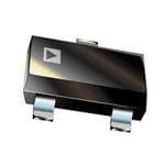
| 产品图片 |
|
| rohs | 符合RoHS无铅 / 符合限制有害物质指令(RoHS)规范要求 |
| 产品系列 | 电源管理 IC,参考电压,Analog Devices AD1584ARTZ-REEL7- |
| 数据手册 | |
| 产品型号 | AD1584ARTZ-REEL7 |
| PCN设计/规格 | |
| 产品目录页面 | |
| 产品种类 | 参考电压 |
| 供应商器件封装 | SOT-23-3 |
| 其它名称 | AD1584ARTZ-REEL7DKR |
| 分流电流—最大值 | 5 mA |
| 初始准确度 | +/- 4 mV |
| 包装 | Digi-Reel® |
| 参考类型 | Series Precision References |
| 商标 | Analog Devices |
| 安装类型 | 表面贴装 |
| 安装风格 | SMD/SMT |
| 容差 | ±0.98% |
| 封装 | Reel |
| 封装/外壳 | TO-236-3,SC-59,SOT-23-3 |
| 封装/箱体 | SOT-23 |
| 工作温度 | -40°C ~ 125°C |
| 工厂包装数量 | 3000 |
| 平均温度系数—典型值 | 50 PPM / C |
| 最大工作温度 | + 125 C |
| 最小工作温度 | - 40 C |
| 标准包装 | 1 |
| 温度系数 | 100ppm/°C |
| 电压-输入 | 4.3 V ~ 12 V |
| 电压-输出 | 4.096V |
| 电流-输出 | 5mA |
| 电流-阴极 | - |
| 电流-静态 | 70µA |
| 电源电流 | 70 uA |
| 系列 | AD1584 |
| 输入电压 | 4.3 V to 12 V |
| 输出电压 | 4.096 V |
| 通道数 | 1 |


- 商务部:美国ITC正式对集成电路等产品启动337调查
- 曝三星4nm工艺存在良率问题 高通将骁龙8 Gen1或转产台积电
- 太阳诱电将投资9.5亿元在常州建新厂生产MLCC 预计2023年完工
- 英特尔发布欧洲新工厂建设计划 深化IDM 2.0 战略
- 台积电先进制程称霸业界 有大客户加持明年业绩稳了
- 达到5530亿美元!SIA预计今年全球半导体销售额将创下新高
- 英特尔拟将自动驾驶子公司Mobileye上市 估值或超500亿美元
- 三星加码芯片和SET,合并消费电子和移动部门,撤换高东真等 CEO
- 三星电子宣布重大人事变动 还合并消费电子和移动部门
- 海关总署:前11个月进口集成电路产品价值2.52万亿元 增长14.8%


PDF Datasheet 数据手册内容提取
2.5 V to 5.0 V Micropower, Precision Series Mode Voltage References Data Sheet AD1582/AD1583/AD1584/AD1585 FEATURES PIN CONFIGURATION Series reference (2.5 V, 3 V, 4.096 V, 5 V) AD1582/ Low quiescent current: 70 μA maximum VOUT 1 AD1583/ Current output capability: ±5 mA AD1584/ AD1585 3 VIN Wide supply range: V = V + 200 mV to 12 V WSpideceibfiaendd t enmoipsee r(a1t0u HrIeNz rtaon 1OgU0eT :k −H4z0):° C50 t oμ V+1 r2m5s° C GND 2 (NToOtPtoVSIEcaWle) 00701-001 Figure 1. 3-Lead SOT-23-3 (RT Suffix) Compact, surface-mount SOT-23 package 900 Qualified for automotive applications 800 APPLICATIONS 700 Portable, battery-powered equipment; for example, 600 notebook computers, cellular phones, pagers, PDAs, GPSs, A) SHUNTREFERENCE1 and DMMs (µY 500 Computer workstations; suitable for use with a wide range PPL 400 U S of video RAMDACs I 300 Smart industrial transmitters 200 PCMCIA cards Automotive 100 AD1582SERIESREFERENCE Hard disk drives 0 3 V/5 V, 8-bit/12-bit data converters 2.7 5 VSUPPLY13(.V0)76kΩSOURCERESISTOR. 00701-002 Figure 2. Supply Current (μA) vs. Supply Voltage (V) GENERAL DESCRIPTION The AD1582/AD1583/AD1584/AD1585 are low cost, low power, The AD1582/AD1583/AD1584/AD1585 series mode devices low dropout, precision band gap references. These designs are source or sink up to 5 mA of load current and operate efficiently available as 3-terminal (series) devices and are packaged in the with only 200 mV of required headroom supply. These parts compact SOT-23, 3-lead surface-mount package. The versatility draw a maximum 70 μA of quiescent current with only a of these references makes them ideal for use in battery-powered 1.0 μA/V variation with supply voltage. The advantage of 3 V or 5 V systems where there can be wide variations in supply these designs over conventional shunt devices is extraordinary. voltage and a need to minimize power dissipation. Valuable supply current is no longer wasted through an input series resistor, and maximum power efficiency is achieved at The superior accuracy and temperature stability of the AD1582/ all input voltage levels. AD1583/AD1584/AD1585 result from the precise matching and thermal tracking of on-chip components. Patented temperature The AD1582/AD1583/AD1584/AD1585 are available in two drift curvature correction design techniques minimize the grades, A and B, and are provided in a tiny footprint, the SOT- nonlinearities in the voltage output temperature characteristic. 23.All grades are specified over the industrial temperature range of −40°C to +125°C. Table 1. AD158x Products, Two Electrical Grades Initial Accuracy Temperature Electrical Coefficient Grade AD1582 AD1583/AD1585 AD1584 (ppm°C) B 0.08% 0.10% 0.10% 50 A 0.80% 1.00% 0.98% 100 Rev. L Document Feedback Information furnished by Analog Devices is believed to be accurate and reliable. However, no responsibility is assumed by Analog Devices for its use, nor for any infringements of patents or other One Technology Way, P.O. Box 9106, Norwood, MA 02062-9106, U.S.A. rights of third parties that may result from its use. Specifications subject to change without notice. No license is granted by implication or otherwise under any patent or patent rights of Analog Devices. Tel: 781.329.4700 ©1997–2018 Analog Devices, Inc. All rights reserved. Trademarks and registered trademarks are the property of their respective owners. Technical Support www.analog.com
AD1582/AD1583/AD1584/AD1585 Data Sheet TABLE OF CONTENTS Features .............................................................................................. 1 Applications Information .............................................................. 12 Applications ....................................................................................... 1 Temperature Performance......................................................... 12 Pin Configuration ............................................................................. 1 Voltage Output Nonlinearity vs. Temperature ....................... 12 General Description ......................................................................... 1 Output Voltage Hysteresis ......................................................... 13 Revision History ............................................................................... 2 Solder Heat Effect ....................................................................... 13 Specifications ..................................................................................... 4 Supply Current vs. Temperature ............................................... 13 AD1582 Specifications ................................................................. 4 Supply Voltage ............................................................................ 13 AD1583 Specifications ................................................................. 5 AC Performance ......................................................................... 13 AD1584 Specifications ................................................................. 6 Noise Performance and Reduction .......................................... 14 AD1585 Specifications ................................................................. 7 Turn-On Time ............................................................................ 14 Absolute Maximum Ratings ............................................................ 8 Dynamic Performance ............................................................... 15 ESD Caution .................................................................................. 8 Outline Dimensions ....................................................................... 16 Terminology ...................................................................................... 9 Ordering Guide .......................................................................... 17 Typical Performance Characteristics ........................................... 10 Automotive Applications ........................................................... 17 Theory of Operation ...................................................................... 11 REVISION HISTORY 5/2018—Rev. K to Rev. L 5/2010—Rev. H to Rev. I Changes to Table 3 ............................................................................ 5 Changes to Figure 10 ...................................................................... 11 Changes to Ordering Guide .......................................................... 17 Updated Outline Dimensions ....................................................... 16 Changes to Ordering Guide .......................................................... 16 10/2017—Rev. J to Rev. K Change to Features and Table 1 Title ............................................. 1 11/2007—Rev. G to Rev. H Changes to Table 2 ............................................................................ 3 Deleted C Grade ................................................................. Universal Changes to Temperature Range Specified Performance Changes to VOERR Parameter ........................................................ 3 Parameter and Temperature Range Operating Performance Changes to Ordering Guide .......................................................... 16 Parameter; Table 3 ............................................................................ 4 Changes to Temperature Range Specified Performance 6/2006—Rev. F to Rev. G Parameter and Temperature Range Operating Performance Changes to Features .......................................................................... 1 Parameter; Table 4 ............................................................................ 5 Changes to General Description ..................................................... 1 Changes to Temperature Range Specified Performance Parameter and Temperature Range Operating Performance 2/2006—Rev. E to Rev. F Parameter; Table 5 ............................................................................ 6 Updated Format .................................................................. Universal Added Solder Heat Effect Section ................................................ 12 Changes to Features .......................................................................... 1 Added Figure 14; Renumbered Sequentially .............................. 12 Changes to Table 6 ............................................................................. 7 Changes to Ordering Guide .......................................................... 16 Changes to Ordering Guide .......................................................... 16 Added Automotive Applications Section .................................... 16 Changes to Package Branding Information Section .................. 16 6/2005—Rev. D to Rev. E Changes to Ordering Guide ............................................................ 7 2/2013—Rev. I to Rev. J Moved Package Branding Section ................................................... 7 Change to Table 6 ............................................................................. 7 Changes to Ordering Guide .......................................................... 16 6/2004—Rev. C to Rev. D Changes to Ordering Guide ............................................................. 6 Updated Outline Dimensions ....................................................... 13 Rev. L | Page 2 of 17
Data Sheet AD1582/AD1583/AD1584/AD1585 12/2002—Rev. B to Rev. C Changes to Features .......................................................................... 1 Changes to General Description ..................................................... 1 Changes to Specifications ................................................................. 2 Changes to Absolute Maximum Ratings ........................................ 6 Replaced TPC 3 ................................................................................. 8 Changes to Temperature Performance Section ............................. 9 Replaced Figure 4 .............................................................................. 9 Changes to Output Voltage Hysteresis Section ........................... 10 Updated SOT-23 Package ............................................................... 13 3/1997—Revision 0: Initial Version Rev. L | Page 3 of 17
AD1582/AD1583/AD1584/AD1585 Data Sheet SPECIFICATIONS AD1582 SPECIFICATIONS T = T to T , V = 5 V, unless otherwise noted. A MIN MAX IN Table 2. AD1582A AD1582B Parameter Min Typ Max Min Typ Max Unit OUTPUT VOLTAGE (at 25°C) V 2.480 2.500 2.520 2.498 2.500 2.502 V O INITIAL ACCURACY ERROR (at 25°C) V −20 +20 −2 +2 mV OERR −0.80 +0.80 −0.08 +0.08 % V (W-Grade) −6 +6 mV OERR −0.24 +0.24 % OUTPUT VOLTAGE TEMPERATURE DRIFT 100 50 ppm/°C TEMPERATURE COEFFICIENT (TCV ) O −40°C < T < +125°C 40 100 18 50 ppm/°C A 0°C < T < 70°C 35 15 ppm/°C A MINIMUM SUPPLY HEADROOM (V − V ) 200 200 mV IN OUT LOAD REGULATION 0 mA < I < 5 mA (−40°C to +85°C) 0.2 0.2 mV/mA OUT 0 mA < I < 5 mA (−40°C to +125°C) 0.4 0.4 mV/mA OUT −5 mA < I < 0 mA (−40°C to +85°C) 0.25 0.25 mV/mA OUT −5 mA < I < 0 mA (−40°C to +125°C) 0.45 0.45 mV/mA OUT −0.1 mA < I < +0.1 mA (−40°C to +85°C) 2.7 2.7 mV/mA OUT −0.1 mA < I < +0.1 mA (−40°C to +125°C) 3.5 3.5 mV/mA OUT LINE REGULATION V + 200 mV < V < 12 V OUT IN I = 0 mA 25 25 µV/V OUT RIPPLE REJECTION (ΔV /ΔV ) OUT IN V = 5 V ± 100 mV (f = 120 Hz) 80 80 dB IN QUIESCENT CURRENT 70 70 µA SHORT-CIRCUIT CURRENT TO GROUND 15 15 mA NOISE VOLTAGE (at 25°C) 0.1 Hz to 10 Hz 70 70 µV p-p 10 Hz to 10 kHz 50 50 µV rms TURN-ON SETTLING TIME TO 0.1% C = 0.2 µF 100 100 µs L LONG-TERM STABILITY 1000 Hours at 25°C 100 100 ppm/1000 hr OUTPUT VOLTAGE HYSTERESIS 115 115 ppm TEMPERATURE RANGE Specified Performance (A, B) −40 +125 −40 +125 °C Operating Performance (A, B) −55 +125 −55 +125 °C Rev. L | Page 4 of 17
Data Sheet AD1582/AD1583/AD1584/AD1585 AD1583 SPECIFICATIONS T = T to T , V = 5 V, unless otherwise noted. A MIN MAX IN Table 3. AD1583A AD1583B Parameter Min Typ Max Min Typ Max Unit OUTPUT VOLTAGE (at 25°C) V 2.970 3.000 3.030 2.997 3.000 3.003 V O INITIAL ACCURACY ERROR (at 25°C) V −30 +30 −3 +3 mV OERR −1.0 +1.0 −0.1 +0.1 % V (W Grade) −8 +8 mV OERR −0.27 +0.27 % OUTPUT VOLTAGE TEMPERATURE DRIFT 100 50 ppm/°C TEMPERATURE COEFFICIENT (TCV ) O −40°C < T < +125°C 40 100 18 50 ppm/°C A 0°C < T < 70°C 35 15 ppm/°C A MINIMUM SUPPLY HEADROOM (V − V ) 200 200 mV IN OUT LOAD REGULATION 0 mA < I < 5 mA (−40°C to +85°C) 0.25 0.25 mV/mA OUT 0 mA < I < 5 mA (−40°C to +125°C) 0.45 0.45 mV/mA OUT −5 mA < I < 0 mA (−40°C to +85°C) 0.40 0.40 mV/mA OUT −5 mA < I < 0 mA (−40°C to +125°C) 0.6 0.6 mV/mA OUT −0.1 mA < I < +0.1 mA (−40°C to +85°C) 2.9 2.9 mV/mA OUT −0.1 mA < I < +0.1 mA (−40°C to +125°C) 3.7 3.7 mV/mA OUT LINE REGULATION V + 200 mV < V < 12 V OUT IN I = 0 mA 25 25 µV/V OUT RIPPLE REJECTION (ΔV /ΔV ) OUT IN V = 5 V ± 100 mV (f = 120 Hz) 80 80 dB IN QUIESCENT CURRENT 70 70 µA SHORT-CIRCUIT CURRENT TO GROUND 15 15 mA NOISE VOLTAGE (at 25°C) 0.1 Hz to 10 Hz 85 85 µV p-p 10 Hz to 10 kHz 60 60 µV rms TURN-ON SETTLING TIME TO 0.1% C = 0.2 µF 120 120 µs L LONG-TERM STABILITY 1000 Hours at 25°C 100 100 ppm/1000 hr OUTPUT VOLTAGE HYSTERESIS 115 115 ppm TEMPERATURE RANGE Specified Performance (A, B) −40 +125 −40 +125 °C Operating Performance (A, B) −55 +125 −55 +125 °C Rev. L | Page 5 of 17
AD1582/AD1583/AD1584/AD1585 Data Sheet AD1584 SPECIFICATIONS T = T to T , V = 5 V, unless otherwise noted. A MIN MAX IN Table 4. AD1584A AD1584B Parameter Min Typ Max Min Typ Max Unit OUTPUT VOLTAGE (at 25°C) V 4.056 4.096 4.136 4.092 4.096 4.100 V O INITIAL ACCURACY ERROR (at 25°C) V −40 +40 −4 +4 mV OERR −0.98 +0.98 −0.1 +0.1 % OUTPUT VOLTAGE TEMPERATURE DRIFT 100 50 ppm/°C TEMPERATURE COEFFICIENT (TCV ) O −40°C < T < +125°C 40 100 18 50 ppm/°C A 0°C < T < 70°C 35 15 ppm/°C A MINIMUM SUPPLY HEADROOM (V − V ) 200 200 mV IN OUT LOAD REGULATION 0 mA < I < 5 mA (−40°C to +85°C) 0.32 0.32 mV/mA OUT 0 mA < I < 5 mA (−40°C to +125°C) 0.52 0.52 mV/mA OUT −5 mA < I < 0 mA (−40°C to +85°C) 0.40 0.40 mV/mA OUT −5 mA < I < 0 mA (−40°C to +125°C) 0.6 0.6 mV/mA OUT −0.1 mA < I < +0.1 mA (−40°C to +85°C) 3.2 3.2 mV/mA OUT −0.1 mA < I < +0.1 mA (−40°C to +125°C) 4.1 4.1 mV/mA OUT LINE REGULATION V + 200 mV < V 12 V OUT IN I = 0 mA 25 25 µV/V OUT RIPPLE REJECTION (ΔV /ΔV ) OUT IN V = 5 V ± 100 mV (f = 120 Hz) 80 80 dB IN QUIESCENT CURRENT 70 70 µA SHORT-CIRCUIT CURRENT TO GROUND 15 15 mA NOISE VOLTAGE (at 25°C) 0.1 Hz to 10 Hz 110 110 µV p-p 10 Hz to 10 kHz 90 90 µV rms TURN-ON SETTLING TIME TO 0.1% C = 0.2 µF 140 140 µs L LONG-TERM STABILITY 1000 Hours at 25°C 100 100 ppm/1000 hr OUTPUT VOLTAGE HYSTERESIS 115 115 ppm TEMPERATURE RANGE Specified Performance (A, B) −40 +125 −40 +125 °C Operating Performance (A, B) −55 −125 −55 +125 °C Rev. L | Page 6 of 17
Data Sheet AD1582/AD1583/AD1584/AD1585 AD1585 SPECIFICATIONS T = T to T , V = 6 V, unless otherwise noted. A MIN MAX IN Table 5. AD1585A AD1585B Parameter Min Typ Max Min Typ Max Unit OUTPUT VOLTAGE (at 25°C) V 4.950 5.000 5.050 4.995 5.000 5.005 V O INITIAL ACCURACY ERROR (at 25°C) V −50 +50 −5 +5 mV OERR −1.0 +1.0 −0.10 +0.10 % OUTPUT VOLTAGE TEMPERATURE DRIFT 100 50 ppm/°C TEMPERATURE COEFFICIENT (TCV ) O −40°C < T < 125°C 40 100 18 50 ppm/°C A 0°C < T < 70°C 35 15 ppm/°C A MINIMUM SUPPLY HEADROOM (V − V ) 200 200 mV IN OUT LOAD REGULATION 0 mA < I < 5 mA (−40°C to +85°C) 0.40 0.40 mV/mA OUT 0 mA < I < 5 mA (−40°C to +125°C) 0.6 0.6 mV/mA OUT −5 mA < I < 0 mA (−40°C to +85°C) 0.40 0.40 mV/mA OUT −5 mA < I < 0 mA (−40°C to +125°C) 0.6 0.6 mV/mA OUT −0.1 mA < I < +0.1 mA (−40°C to +85°C) 4 4 mV/mA OUT −0.1 mA < I < +0.1 mA (−40°C to +125°C) 4.8 4.8 mV/mA OUT LINE REGULATION V + 200 mV < V < 12 V OUT IN I = 0 mA 25 25 µV/V OUT RIPPLE REJECTION (ΔV /ΔV ) OUT IN V = 6 V ± 100 mV (f = 120 Hz) 80 80 dB IN QUIESCENT CURRENT 70 70 µA SHORT-CIRCUIT CURRENT TO GROUND 15 15 mA NOISE VOLTAGE (at 25°C) 0.1 Hz to 10 Hz 140 140 µV p-p 10 Hz to 10 kHz 100 100 µV rms TURN-ON SETTLING TIME TO 0.1% C = 0.2 μF 175 175 µs L LONG-TERM STABILITY 1000 Hours at 25°C 100 100 ppm/1000 hr OUTPUT VOLTAGE HYSTERESIS 115 115 ppm TEMPERATURE RANGE Specified Performance (A, B) −40 +125 −40 +125 °C Operating Performance (A, B) −55 +125 −55 +125 °C Rev. L | Page 7 of 17
AD1582/AD1583/AD1584/AD1585 Data Sheet ABSOLUTE MAXIMUM RATINGS Table 6. Stresses at or above those listed under Absolute Maximum Parameter Rating Ratings may cause permanent damage to the product. This is a V to Ground 12 V stress rating only; functional operation of the product at these IN Internal Power Dissipation1 or any other conditions above those indicated in the operational SOT-23-3 (RT-3) 400 mW section of this specification is not implied. Operation beyond Storage Temperature Range −65°C to 150°C the maximum operating conditions for extended periods may Specified Temperature Range affect product reliability. AD1582RT/AD1583RT/ −40°C to +125°C ESD CAUTION AD1584RT/AD1585RT Lead Temperature, Soldering Vapor Phase (60 sec) 215°C Infrared (15 sec) 220°C 1 Specification is for device in free air at 25°C; SOT-23 package, θJA = 300°C. Rev. L | Page 8 of 17
Data Sheet AD1582/AD1583/AD1584/AD1585 TERMINOLOGY Thermal Hysteresis (V ) Temperature Coefficient (TCV ) O_HYS O The change of output voltage after the device is cycled through The change of output voltage over the operating temperature temperatures from +25°C to −40°C to +85°C and back to +25°C. change and normalized by the output voltage at 25°C, expressed This is a typical value from a sample of parts put through in ppm/°C. The equation follows such a cycle V (T )−V (T ) TCV [ppm/°C]= O 2 O 1 ×10⁶ V =V (25°C)−V O V (25°C)×(T −T ) O_HYS O O_TC O 2 1 V (25°C)−V where: V [ppm]= O O_TC ×106 VO (25°C) = VO at 25°C. O_HYS VO(25°C) V (T) = V at Temperature 1. O 1 O where: V (T) = V at Temperature 2. O 2 O V (25°C) = V at 25°C. O O Line Regulation (ΔVO/ΔVIN) Definition VO_TC = VO at 25°C after temperature cycle at +25°C to −40°C to The change in output voltage due to a specified change in input +85°C and back to +25°C. voltage. It includes the effects of self-heating. Line regulation is Operating Temperature expressed in either percent per volt, parts per million per volt, The temperature extremes at which the device can still function. or microvolts per volt change in input voltage. Parts can deviate from their specified performance outside the Load Regulation (ΔV /ΔI ) specified temperature range. O LOAD The change in output voltage due to a specified change in load current. It includes the effects of self-heating. Load regulation is expressed in either microvolts per milliampere, parts per million per milliampere, or ohms of dc output resistance. Long-Term Stability (ΔV ) O Typical shift of output voltage at 25°C on a sample of parts subjected to an operation life test of 1000 hours at 125°C. ∆V =V (t )−V (t ) O O 0 O 1 V (t )−V (t ) ∆V [ppm]= O 0 O 1 ×10⁶ O V (t ) O 0 where: V (t) = V at 25°C at Time 0. O 0 O V (t) = V at 25°C after 1000 hours of operation at 125°C. O 1 O Rev. L | Page 9 of 17
AD1582/AD1583/AD1584/AD1585 Data Sheet TYPICAL PERFORMANCE CHARACTERISTICS 0.40 22 20 0.35 18 0.30 S 16 AD1585 T AR 14 0.25 ER OF P 1120 mV/mA 0.20 AD1582 B M 0.15 U 8 N 6 0.10 4 0.05 2 0–60 –50 –40 –30 –20 –p1p0m/°C0 10 20 30 40 50 00701-003 00 2 4 VIN6(V) 8 10 12 00701-006 Figure 3. Typical Output Voltage Temperature Drift Distribution Figure 6. Load Regulation vs. VIN 50 0 45 –10 40 –20 TS 35 –30 R A 30 F P V –40 ER O 25 µV/ –50 AD1582 B 20 M U –60 N 15 AD1585 –70 10 5 –80 0 –90 –1.0% –0.6% –0V.2O%UT(ERRO0.R2%) 0.6% 1.0% 00701-004 –5 –4 –3 –2 –1IOUT0(mA)1 2 3 4 5 00701-007 Figure 4. Typical Output Voltage Error Distribution Figure 7. Line Regulation vs. ILOAD 2.504 10k 2.502 2.500 2.498 IOUT = 1mA VOUT2.496 V/ Hz 1k IOUT = 0mA n 2.494 2.492 2.490 2.488–40 –20 0 T20EMPER40ATURE60(°C) 80 100 120 00701-005 10010 100 FREQUE1kNCY (Hz) 10k 100k 00701-008 Figure 5. Typical Temperature Drift Characteristic Curves Figure 8. Noise Spectral Density Rev. L | Page 10 of 17
Data Sheet AD1582/AD1583/AD1584/AD1585 THEORY OF OPERATION The AD1582/AD1583/AD1584/AD1585 use the band gap concept to produce stable, low temperature coefficient voltage VIN references suitable for high accuracy data acquisition compo- R3 R4 nents and systems. These parts of precision references use the underlying temperature characteristics of a silicon transistor’s VOUT base emitter voltage in the forward-biased operating region. R5 Under this condition, all such transistors have a −2 mV/°C VBG temperature coefficient (TC) and a V that, when extrapolated BE + to absolute zero, 0 K (with collector current proportional to VBE R2 R6 – absolute temperature), approximates the silicon band gap voltage. + Btuyr es ucmoemffiincige nat v oofl t2a gme Vth/°aCt h waist han t heeq uVaBlE aonfd a ofoprpwoasirtde- tbeimaspeedr a- R1 V–1 GND 00701-009 transistor, an almost 0 TC reference can be developed. In the Figure 9. Simplified Schematic AD1582/AD1583/AD1584/AD1585 simplified circuit diagram shown in Figure 9, such a compensating voltage, V1, is derived by driving two transistors at different current densities and amplifying the resultant V difference (∆V , which has a positive BE BE TC). The sum of V and V1 (V ) is then buffered and amplified BE BG to produce stable reference voltage outputs of 2.5 V, 3 V, 4.096 V, and 5 V. Rev. L | Page 11 of 17
AD1582/AD1583/AD1584/AD1585 Data Sheet APPLICATIONS INFORMATION Duplication of these results requires a test system that is highly The AD1582/AD1583/AD1584/AD1585 are series references accurate with stable temperature control. Evaluation of the that can be used for many applications. To achieve optimum AD1582/AD1583/AD1584/AD1585 produces curves similar performance with these references, only two external compo- to those in Figure 5 and Figure 11, but output readings can vary nents are required. Figure 10 shows the AD1582/AD1583/ depending on the test methods and test equipment used. AD1584/AD1585 configured for operation under all loading conditions. With a simple 4.7 µF capacitor attached to the input 22..550044 and a 1 µF capacitor applied to the output, the devices can achieve 22..550022 specified performance for all input voltage and output current requirements. For best transient response, add a 0.1 µF capacitor 22..550000 in parallel with the 4.7 µF capacitor. While a 1 µF output capacitor can provide stable performance for all loading conditions, the V)V) AD1582/AD1583/AD1584/AD1585 can operate under low ( (OUTOUT22..449988 VV (−100 µA < I < +100 µA) current conditions with just a OUT 22..449966 0.2 µF output capacitor. The 4.7 µF capacitor on the input can be reduced to 1 μF in this condition. 22..449944 Unlike conventional shunt reference designs, the AD1582/ AD1583/AD1584/AD1585 provide stable output voltages at 22..449922 caos nshstoawntn o ipne Friagtuinrge c1u0r, rtehnets ele dveevlsi.c Wes hcaenn bpero appeprlliye dd etcoo aunpyl ed, ––4400 ––2200 00 TT22EE00MMPPEERR44AA00TTUURREE66((00°°CC)) 8800 110000 112200 00701-011 Figure 11. Output Voltage vs. Temperature circuit and provide superior low power solutions. VOLTAGE OUTPUT NONLINEARITY VS. TEMPERATURE + 1 AD1582/ AD1583/ When using a voltage reference with data converters, it is VOUT 1µF AD1584/ 3 VIN AD1585 4.7µF important to understand the impact that temperature drift can – 2 00701-010 houavtpe uotn d croifntv reerpterre speenrftos ramddanitcieo.n Tahl ee rnroonr ltinheaat rcitayn onfo tth bee r eefaesrielny ce Figure 10. Typical Connection Diagram calibrated out of the overall system. To better understand the TEMPERATURE PERFORMANCE impact such a drift can have on a data converter, refer to Figure 12, where the measured drift characteristic is normalized to the The AD1582/AD1583/AD1584/AD1585 are designed for endpoint average drift. The residual drift error for the AD1582/ applications where temperature performance is important. AD1583/AD1584/AD1585 of approximately 200 ppm demon- Extensive temperature testing and characterization ensure strates that these parts are compatible with systems that require that device performance is maintained over the specified 12-bit accurate temperature performance. temperature range. 250 The error band guaranteed with the AD1582/AD1583/AD1584/ AD1585 is the maximum deviation from the initial value at 25°C. 200 Therefore, for a given grade of the AD1582/AD1583/AD1584/ AD1585, the designer can easily determine the maximum total 150 error by summing initial accuracy and temperature variation. For m) p example, for the AD1582BRT, the initial tolerance is ±2 mV, and (pUT 100 the temperature error band is ±8 mV; therefore, the reference is O V Δ guaranteed to be 2.5 V ± 10 mV from −40°C to +125°C. 50 Figure 11 shows the typical output voltage drift for the AD1582/ AD1583/AD1584/AD1585 and illustrates the methodology. The 0 box in Figure 11 is bounded on the x-axis by operating tempera- taunrde mexitnriemmuems. Iot uistp buotu vnodlteadg eosn o tbhsee ryv-aexdi so vbeyr tthhee mopaexrimatiunmg –50–50 –25 0TEMPERA25TURE(°C5)0 75 100 00701-012 temperature range. The slope of the diagonal drawn from the Figure 12. Residual Drift Error initial output value at 25°C to the output values at +125°C and −40°C determines the performance grade of the device. Rev. L | Page 12 of 17
Data Sheet AD1582/AD1583/AD1584/AD1585 OUTPUT VOLTAGE HYSTERESIS SUPPLY CURRENT VS. TEMPERATURE High performance industrial equipment manufacturers can The quiescent current for the AD1582/AD1583/AD1584/ require the AD1582/AD1583/AD1584/AD1585 to maintain a AD1585 varies slightly over temperature and input supply consistent output voltage error at 25°C after the references are range. Figure 15 illustrates the typical performance for the operated over the full temperature range. All references exhibit AD1582/AD1583/AD1584/AD1585 reference when varying a characteristic known as output voltage hysteresis; however, the both temperature and supply voltage. As is evident from AD1582/AD1583/AD1584/AD1585 are designed to minimize Figure 15, the AD1582/AD1583/AD1584/AD1585 supply this characteristic. This phenomenon can be quantified by mea- current increases only 1.0 µA/V, making this device extremely suring the change in the +25°C output voltage after temperature attractive for use in applications where there can be wide excursions from +125°C to +25°C and from −40°C to +25°C. variations in supply voltage and a need to minimize power Figure 13 displays the distribution of the AD1582/AD1583/ dissipation. AD1584/AD1585 output voltage hysteresis. 100 80 70 80 60 TS 60 TA=+85°C TA=+25°C R OF PAR 5400 I (µA)Q 40 E B M 30 U TA=–40°C N 20 20 10 0–700 –450 –200 ppm50 300 550 00701-013 03Figure4 15. Typ5ical Su6pplyV CINu7(rVre)nt o8ver Tem9perat1u0re 11 00701-014 Figure 13. Output Voltage Hysteresis Distribution SOLDER HEAT EFFECT SUPPLY VOLTAGE The mechanical stress and heat effect of soldering a device to a One of the ideal features of the AD1582/AD1583/AD1584/AD1585 printed circuit board (PCB) can cause the output voltage of a is low supply voltage headroom. The parts can operate at supply reference to shift in value. The materials that make up a voltages as low as 200 mV above V and up to 12 V. However, OUT semiconductor device and its package have different rates of if negative voltage is inadvertently applied to V with respect to IN expansion and contraction. If the stress on the die has changed ground, or any negative transient >5 V is coupled to V , the IN position, it can cause a shift on the output voltage after being device can be damaged. exposed to extreme soldering temperatures. This shift is similar AC PERFORMANCE to, but more severe than, thermal hysteresis. Typical result of soldering temperature effects on the AD1582/ To apply the AD1582/AD1583/AD1584/AD1585, it is impor- AD1583/AD1584/AD1585 output values shift is shown in tant to understand the effects of dynamic output impedance Figure 14. Figure 14 shows the output shift due to soldering and and power supply rejection. In Figure 16, a voltage divider does not include mechanical stress. is formed by the AD1582/AD1583/AD1584/ AD1585 output 60 impedance and by the external source impedance. Figure 17 shows the effect of varying the load capacitor on the reference 50 output. Power supply rejection ratio (PSRR) should be determined when characterizing the ac performance of a series voltage TS40 reference. Figure 18 shows a test circuit used to measure PSRR, NI F U and Figure 19 demonstrates the ability of the AD1582/AD1583/ R O30 AD1584/AD1585 to attenuate line voltage ripple. E B NUM20 VLOADDC 5V 2kΩ 10kΩ 10 2×VOUT 10kΩ ×1 DUT 5µF –00.20 –0O.U15TPU–T0 .S10HFT– D0.U05ETO S0OLDER0 .H05EAT 0E.F1F0ECT0 (.%15) 0.20 00701-114 ±2V 10FkiΩgure 16. Outp±u10t 0ImµApedanc1eµ FTest Circuit 00701-015 Figure 14. Output Shift due to Solder Heat Effect Rev. L | Page 13 of 17
AD1582/AD1583/AD1584/AD1585 Data Sheet 100 10µV 1s 1µFCAP 100 Ω) 90 E ( 10 C N DA AD1585 E P M T I AD1582 U TP 1 OU 10 0% 0.110 100 F1RkEQUENCY1(0Hkz) 100k 1M 00701-016 Figure 20. 10 Hz to 10 kHz Wideband Noise 00701-019 Figure 17. Output Impedance vs. Frequency 10V 10kΩ 5V±100mV 100µV 10ms ×1 ±200mV 10kΩ 0.22µF DUT VOUT 19000 0.22µF 00701-017 Figure 18. Ripple Rejection Test Circuit 100 90 10 0% 80 70 AD1582 00701-020 B) 60 Figure 21. 1 Hz to 10 Hz Voltage Noise d R ( 50 SR AD1585 TURN-ON TIME P 40 Many low power instrument manufacturers are concerned 30 with the turn-on characteristics of the components used in their 20 systems. Fast turn-on components often enable the end user to 10 save power by keeping power off when not needed. Turn-on 01 10 100FREQU1EkNCY(Hz)10k 100k 1M 00701-018 speotwtlienrg ( tciomlde isst adretf)i,n feodr atsh teh oeu titmpuet r veoqlutiargeed ,t oaf rteera cthhe i atsp pfilnicaalt vioanlu oef Figure 19. Ripple Rejection vs. Frequency within a specified error. The two major factors affecting this are the active circuit settling time and the time required for the NOISE PERFORMANCE AND REDUCTION thermal gradients on the chip to stabilize. Figure 22 shows the The noise generated by the AD1582/AD1583/AD1584/AD1585 is turn-on settling and transient response test circuit. Figure 23 typically less than 70 µV p-p over the 0.1 Hz to 10 Hz frequency shows the turn-on characteristics of the AD1582/AD1583/ band. Figure 20 shows the 0.1 Hz to 10 Hz noise of a typical AD1584/AD1585. These characteristics are generated from cold- AD1582/AD1583/AD1584/AD1585. The noise measurement start operation and represent the true turn-on waveform after is made with a high gain band-pass filter. Noise in a 10 Hz to power-up. Figure 24 shows the fine settling characteristics of 10 kHz region is approximately 50 µV rms. Figure 21 shows the the AD1582/AD1583/AD1584/AD1585. Typically, the reference broadband noise of a typical AD1582/AD1583/AD1584/AD1585. settles to within 0.1% of its final value in about 100 µs. If further noise reduction is desired, add a 1-pole, low-pass The device can momentarily draw excessive supply current filter between the output pin and ground. A time constant of when V is slightly below the minimum specified level. SUPPLY 0.2 ms has a −3 dB point at roughly 800 Hz and reduces the Power supply resistance must be low enough to ensure reliable high frequency noise to about 16 V rms. It should be noted, turn-on. Fast power supply edges minimize this effect. however, that while additional filtering on the output can improve the noise performance of the AD1582/AD1583/ AD1584/AD1585, the added output impedance can degrade the ac performance of the references. Rev. L | Page 14 of 17
Data Sheet AD1582/AD1583/AD1584/AD1585 0V OR10V 10kΩ Figure 26 and Figure 27 show the load transient settling cha- 5V OR10V 0V OR5V racteristics for the AD1582/AD1583/AD1584/AD1585 when 0VTO10V 10kΩ 0.22µF VOUT load current steps of 0 mA to +5 mA and 0 mA to −1 mA are DUT applied. The input supply voltage remains constant at 5 V; the 0.22µF 00701-021 irnepspuet cdteivcoeluyp; lainngd atnhde oouuttppuutt lcouardr ecnapt aisc ittoogrgs laerde. 4F.o7r μbFo tahn dp o1s μitFiv, e Figure 22. Turn-On/Transient Response Test Circuit and negative current loads, the reference responses settle very quickly and exhibit initial voltage spikes of less than 10 mV. 5V 20µs 100 5V 50µs 90 100 90 10 0% 10 F1igVure 23. Turn-On Characteri2s0tiµcss 00701-022 0% 200mV 50µs 00701-024 Figure 25. Line Transient Response 5V 20µs 100 5V 20µs 90 100 90 10 0% 10 1mFVigure 24. Turn-On Settling2 0µs 00701-023 0% 5mV 20µs 00701-025 DYNAMIC PERFORMANCE Figure 26. Load Transient Response (0 mA to 5 mA Load) Many ADCs and DACs present transient current loads to the 20µs reference and poor reference response can degrade converter 5V performance. The AD1582/AD1583/AD1584/AD1585 provide 100 superior static and dynamic line and load regulation. Because 90 these series references are capable of both sourcing and sinking large current loads, they exhibit excellent settling charac- teristics. Figure 25 displays the line transient response for the AD1582/ AD1583/AD1584/AD1585. The circuit used to perform such 10 a measurement is shown in Figure 22, where the input supply 0% vcaopltaacgieto irss t oargeg leeadc hfr 0o.m22 5 μ VF. to 10 V, and the input and output 5mV 20µs 00701-026 Figure 27. Load Transient Response (0 mA to −1 mA Load) Rev. L | Page 15 of 17
AD1582/AD1583/AD1584/AD1585 Data Sheet OUTLINE DIMENSIONS 3.04 2.90 2.80 1.40 1.30 1.20 3 2.64 2.10 1 2 0.60 1.03 0.45 0.89 2.05 1.02 1.78 0.95 0.54 REF 0.88 1.12 GAUGE 0.89 PLANE 0.100 0.180 0.013 0.085 0.51 SEPALTAINNGE 0.37 0.25 0.60 MAX 0.30 MIN COMPLIANTTO JEDEC STANDARDSTO-236-AB 011909-C Figure 28. 3-Lead Small Outline Transistor Package [SOT-23-3] (RT-3) Dimensions shown in millimeters 4.10 7” REEL 100.00 1.10 OR 4.00 1.00 13” REEL 330.00 14.40 MIN 1.55 3.90 2.05 1.10 0.90 1.50 2.00 1.00 0.35 1.45 1.95 0.90 0.30 0.25 1.50 MIN 7” REEL 50.00 MIN 8.30 2.80 20.20 13.20 OR 2.70 MIN 13.00 13” REEL 100.00 MIN 8.00 2.60 12.80 7.70 3.55 3.50 3.45 3.20 0.75 MIN 1.00 MIN 3.10 2.90 9.90 8.40 DIRECTION OF UNREELING 6.90 053006-0 Figure 29. SOT-23 Tape and Reel Outline Dimension (RT-3) Dimensions shown in millimeters Rev. L | Page 16 of 17
Data Sheet AD1582/AD1583/AD1584/AD1585 ORDERING GUIDE No. of Parts Output Initial Initial Temp. Package Package Marking Banding Model1,2 Voltage (V) Accuracy (mV) Accuracy (%) Coefficient (ppm/°C) Description Option Code per Reel AD1582ARTZ-REEL7 2.50 20 0.80 100 SOT-23-3 RT-3 R1Z 3,000 AD1582BRTZ-REEL7 2.50 2 0.08 50 SOT-23-3 RT-3 R20 3,000 AD1582WBRTZ-R7 2.50 6 0.24 50 SOT-23-3 RT-3 R20 3,000 AD1583ARTZ-REEL7 3.00 30 1.00 100 SOT-23-3 RT-3 R22 3,000 AD1583BRTZ-REEL7 3.00 3 0.10 50 SOT-23-3 RT-3 R23 3,000 AD1583WBRTZ-R7 3.00 8 0.27 50 SOT-23-3 RT-3 R23 3,000 AD1584ARTZ-REEL7 4.096 40 0.98 100 SOT-23-3 RT-3 R25 3,000 AD1584BRTZ-REEL7 4.096 4 0.10 50 SOT-23-3 RT-3 R26 3,000 AD1585ARTZ-REEL7 5.00 50 1.00 100 SOT-23-3 RT-3 R28 3,000 AD1585BRTZ-REEL7 5.00 5 0.10 50 SOT-23-3 RT-3 R29 3,000 1 Z = RoHS Compliant Part. 2 W = Qualified for Automotive Applications. AUTOMOTIVE APPLICATIONS The AD1582W and AD1583W models are available with controlled manufacturing to support the quality and reliability requirements of automotive applications. Note that these models may have specifications that differ from the commercial models; therefore, designers should review the Specifications section of this data sheet carefully. Only the automotive grade products shown are available for use in automotive applications. Contact your local Analog Devices account representative for specific product ordering information and to obtain the specific Automotive Reliability reports for these models. ©1997–2018 Analog Devices, Inc. All rights reserved. Trademarks and registered trademarks are the property of their respective owners. D00701-0-5/18(L) Rev. L | Page 17 of 17
Mouser Electronics Authorized Distributor Click to View Pricing, Inventory, Delivery & Lifecycle Information: A nalog Devices Inc.: AD1585ARTZ-REEL7 AD1582ARTZ-R2 AD1583ARTZ-R2 AD1584ARTZ-REEL7 AD1583BRTZ-REEL7 AD1585BRTZ-REEL7 AD1582ART-REEL7 AD1583ARTZ-REEL7 AD1584ARTZ-R2 AD1584BRTZ-REEL7 AD1582ARTZ-REEL7 AD1585ARTZ-R2 AD1582BRTZ-REEL7 AD1582WBRTZ-R7 AD1583WBRTZ-R7