ICGOO在线商城 > 集成电路(IC) > 时钟/计时 - 实时时钟 > AB0805-T3
 Datasheet下载
- 型号: AB0805-T3
- 制造商: ABRACON
- 库位|库存: xxxx|xxxx
- 要求:
| 数量阶梯 | 香港交货 | 国内含税 |
| +xxxx | $xxxx | ¥xxxx |
查看当月历史价格
查看今年历史价格
AB0805-T3产品简介:
ICGOO电子元器件商城为您提供AB0805-T3由ABRACON设计生产,在icgoo商城现货销售,并且可以通过原厂、代理商等渠道进行代购。 AB0805-T3价格参考。ABRACONAB0805-T3封装/规格:时钟/计时 - 实时时钟, Real Time Clock (RTC) IC Clock/Calendar 256B I²C, 2-Wire Serial 16-VFQFN Exposed Pad。您可以下载AB0805-T3参考资料、Datasheet数据手册功能说明书,资料中有AB0805-T3 详细功能的应用电路图电压和使用方法及教程。
Abracon LLC的AB0805-T3是一款实时时钟(RTC)模块,属于时钟/计时器件类别。该型号采用小型8引脚陶瓷封装(如8-SOIC),具有高精度和低功耗特性,适用于需要长时间稳定时间记录的应用场景。

AB0805-T3主要应用于对时间精度要求较高的工业控制设备,如数据采集系统、PLC(可编程逻辑控制器)和工业自动化仪表。在通信设备中,它为网络交换机、路由器等提供可靠的时间基准,确保日志记录与同步操作准确无误。此外,该器件也广泛用于医疗仪器,如监护仪和诊断设备,以保障事件时间戳的准确性。

消费类电子产品如智能电表、安防监控系统和智能家居中枢设备也常采用AB0805-T3,因其在断电情况下可通过备用电池维持时间运行,保证系统时间不丢失。其稳定的温度特性和抗干扰能力,使其在复杂电磁环境中仍能可靠工作。

总之,AB0805-T3适用于需长时间、高可靠性时间保持的嵌入式系统,尤其适合工业、通信、医疗及智能计量等领域。
| 参数 | 数值 |
| 3D型号 | 点击此处下载产品Datasheethttp://www.abracon.com/Support/STEP/Precisiontiming/AB08XX.STEP.zip |
| 产品目录 | 集成电路 (IC)半导体 |
| 描述 | IC RTC CLK/CALENDAR I2C 16-QFN实时时钟 Interface I2C HH:MM:SS:hh 12/24 hr |
| 产品分类 | |
| 品牌 | ABRACON |
| 产品手册 | |
| 产品图片 |
|
| rohs | 符合RoHS无铅 / 符合限制有害物质指令(RoHS)规范要求 |
| 产品系列 | 时钟和计时器IC,实时时钟,ABRACON AB0805-T3- |
| 数据手册 | 点击此处下载产品Datasheet点击此处下载产品Datasheet点击此处下载产品Datasheet点击此处下载产品Datasheet |
| 产品型号 | AB0805-T3 |
| RoHS指令信息 | |
| RTC总线接口 | I2C |
| 产品种类 | |
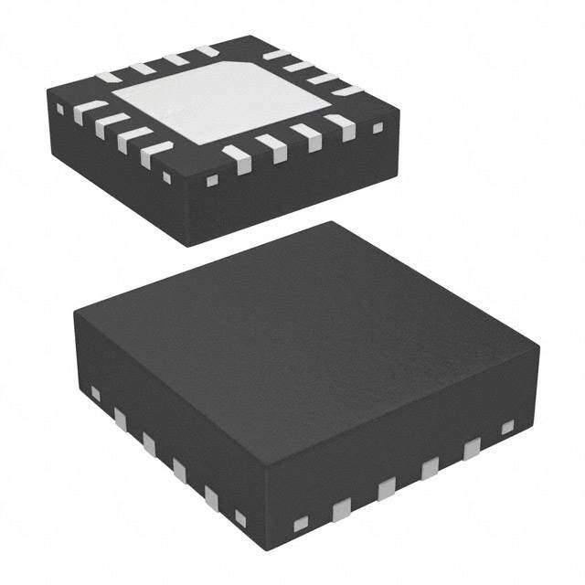
| 供应商器件封装 | 16-QFN(3x3) |
| 其它名称 | 535-11926-2 |
| 功能 | Clock, Calendar, Alarm |
| 包装 | 带卷 (TR) |
| 商标 | ABRACON |
| 存储容量 | 256B |
| 安装类型 | 表面贴装 |
| 安装风格 | SMD/SMT |
| 封装 | Reel |
| 封装/外壳 | 16-VFQFN 裸露焊盘 |
| 封装/箱体 | QFN-16 |
| 工作温度 | -40°C ~ 85°C |
| 工厂包装数量 | 3000 |
| 接口 | I²C,2 线串口 |
| 日期格式 | YY-MM-DD-dd |
| 时间格式 | HH:MM:SS:hh |
| 最大工作温度 | + 85 C |
| 最小工作温度 | - 40 C |
| 标准包装 | 3,000 |
| 特性 | 警报器,闰年,SRAM,涓流充电器,监视计时器 |
| 特色产品 | http://www.digikey.cn/product-highlights/zh/ab-series-realtimeclocks/52319 |
| 电压-电源 | 1.7 V ~ 3.6 V |
| 电压-电源,电池 | 1.5 V ~ 3.6 V |
| 电流-计时(最大) | 0.17µA ~ 0.22µA @ 1.8V ~ 3V |
| 电源电压-最大 | 3.6 V |
| 电源电压-最小 | 1.7 V |
| 类型 | 时钟/日历 |


- 商务部:美国ITC正式对集成电路等产品启动337调查
- 曝三星4nm工艺存在良率问题 高通将骁龙8 Gen1或转产台积电
- 太阳诱电将投资9.5亿元在常州建新厂生产MLCC 预计2023年完工
- 英特尔发布欧洲新工厂建设计划 深化IDM 2.0 战略
- 台积电先进制程称霸业界 有大客户加持明年业绩稳了
- 达到5530亿美元!SIA预计今年全球半导体销售额将创下新高
- 英特尔拟将自动驾驶子公司Mobileye上市 估值或超500亿美元
- 三星加码芯片和SET,合并消费电子和移动部门,撤换高东真等 CEO
- 三星电子宣布重大人事变动 还合并消费电子和移动部门
- 海关总署:前11个月进口集成电路产品价值2.52万亿元 增长14.8%


PDF Datasheet 数据手册内容提取
AB08X5 Real-Time Clock Family Date of Issue: October 16, 2014 3.0 x 3.0 mm Page 1 of 33 Abracon Drawing #453567 Revision: C Features • Ultra-low supply current (all at 3V): - 14 nA with RC oscillator - 22 nA with RC oscillator and Autocalibration - 55 nA with crystal oscillator • Baseline timekeeping features: - 32.768 kHz crystal oscillator with integrated load capacitor/resistor - Counters for hundredths, seconds, minutes, hours, date, month, year, century, and week- Applications day - Alarm capability on all counters • Smart cards - Programmable output clock generation • Wireless sensors and tags (32.768 kHz to 1 year) • Medical electronics - Countdown timer with repeat function • Utility meters - Automatic leap year calculation • Data loggers • Advanced timekeeping features: • Appliances - Integrated power optimized RC oscillator • Handsets - Advanced crystal calibration to ± 2 ppm • Consumer electronics - Advanced RC calibration to ± 16 ppm • Communications equipment - Automatic calibration of RC oscillator to crystal oscillator Description - Watchdog timer with hardware reset - 256 bytes of general purpose RAM The ABRACON AB08X5 Real-Time Clock family • Power management features: provides a groundbreaking combination of ultra-low - Automatic switchover to VBAT power coupled with a highly sophisticated feature - External interrupt monitor set. With power requirements significantly lower than - Programmable low battery detection threshold any other industry RTC (as low as 14 nA), these are - Programmable analog voltage comparator the first semiconductors based on innovative • I2C (up to 400 kHz) and 3-wire or 4-wire SPI (up SPOTTM (Subthreshold Power Optimized to 2 MHz) serial interfaces available Technology) CMOS platform. The AB08X5 includes • Operating voltage 1.5-3.6 V on-chip oscillators to provide minimum power • Clock and RAM retention voltage 1.5-3.6 V consumption, full RTC functions including battery • Operating temperature –40 to 85 °C backup and programmable counters and alarms for • All inputs include Schmitt Triggers timer and watchdog functions, and either an I2C or • 3x3 mm QFN-16 package SPI serial interface for communication with a host controller. Disclaimer: AB08X5 series of devices are based on innovative SPOT technology, proprietary to Ambiq Micro.
AB08X5 Real-Time Clock Family Date of Issue: October 16, 2014 3.0 x 3.0 mm Page 2 of 33 Abracon Drawing #453567 Revision: C 1. Family Summary The AB08X5 family consists of several members (see Table1). All devices are supplied in a standard 3x3 mm QFN-16 package. Members of the software and pin compatible AB18X5 RTC family are also listed. Table 1: Family Summary Baseline Advanced Timekeeping Power Management Timekeeping Part # Calib/ Interface Number Power XT RC Auto- Watch- RAM VBAT Reset Ext of GP Switch and Osc Osc calib dog (B) Switch Mgmt Int Outputs Sleep FSM AB0805 ■ 3 ■ ■ ■ 256 ■ ■ I2C AB0815 ■ 2 ■ ■ ■ 256 ■ ■ SPI Software and Pin Compatible AB18X5 Family Components AB1805 ■ 4 ■ ■ ■ 256 ■ ■ ■ ■ I2C AB1815 ■ 3 ■ ■ ■ 256 ■ ■ ■ ■ SPI
AB08X5 Real-Time Clock Family Date of Issue: October 16, 2014 3.0 x 3.0 mm Page 3 of 33 Abracon Drawing #453567 Revision: C 2. Functional Description Figure1 illustrates the AB08X5 functional design. VCC VBAT 100ths Power Analog Seconds nCE Control Compare Minutes SDI I2C/SPI Hours SCL Interface Days SDA/O Weekdays Months Calibration Engine Years XO Alarms XT Osc Divider Timer WDT XI Control RC Osc Divider RAM WDI FOUT/nIRQ EXTI Int/Clock nIRQ2 nTIRQ VSS Figure 1. Detailed Block Diagram The AB08X5 serves as a full function RTC for host processors such as microcontrollers. The AB08X5 includes 3 distinct feature groups: 1) baseline timekeeping features, 2) advanced timekeeping features, and 3) basic power management features. Functions from each feature group may be controlled via I/O offset mapped registers. These registers are accessed using either an I2C serial interface (e.g., in the AB0805) or a SPI serial interface (e.g., in the AB0815). Each feature group is described briefly below and in greater detail in subsequent sections. The baseline timekeeping feature group supports the standard 32.786 kHz crystal (XT) oscillation mode for maximum frequency accuracy with an ultra-low current draw of 55 nA. The baseline timekeeping feature group also includes a standard set of counters monitoring hundredths of a second up through centuries. A complement of countdown timers and alarms may additionally be set to initiate interrupts or resets on several of the outputs.
AB08X5 Real-Time Clock Family Date of Issue: October 16, 2014 3.0 x 3.0 mm Page 4 of 33 Abracon Drawing #453567 Revision: C The advanced timekeeping feature group supports two additional oscillation modes: 1) RC oscillator mode, and 2) Autocalibration mode. At only 14 nA, the temperature-compensated RC oscillator mode provides an even lower current draw than the XT oscillator for applications with reduced frequency accuracy requirements. A proprietary calibration algorithm allows the AB08X5 to digitally tune the RC oscillator frequency and the XT oscillator frequency with accuracy as low as 2 ppm at a given temperature. In Autocalibration mode, the RC oscillator is used as the primary oscillation source and is periodically calibrated against the XT oscillator. Autocalibration may be done automatically every 8.5 minutes or 17 minutes and may also be initiated via software. This mode enables average current draw of only 22 nA with frequency accuracy similar to the XT oscillator. The advanced timekeeping feature group also includes a rich set of input and output configuration options that enables the monitoring of external interrupts (e.g., pushbutton signals), the generation of clock outputs, and watchdog timer functionality. Power management features built into the AB08X5 enable it to operate as a backup device in both line- powered and battery-powered systems. An integrated power control module automatically detects when main power (VCC) falls below a threshold and switches to backup power (VBAT). 256B of ultra-low leakage RAM enable the storage of key parameters when operating on backup power. The AB08X5 also includes digitally-tunable voltage detection on the backup power supply.
AB08X5 Real-Time Clock Family Date of Issue: October 16, 2014 3.0 x 3.0 mm Page 5 of 33 Abracon Drawing #453567 Revision: C 3. AB08X5 Example Applications 3.1 Battery Backed Up RTC The most common AB08X5 application is a battery backed up RTC, which maintains time and may hold data in RAM. The AB08X5 is normally powered from a system power supply, which may be a larger battery. The AB08X5 is continuously charging a supercapacitor or rechargeable battery via the internal trickle charger. When the main power supply goes away, the AB08X5 automatically switches to the VBAT supply and maintains time and RAM data at very low battery supply currents. System Power 1.5k* VBAT VCC VCC I2C/SPI Battery/ XO Supercap AB08X5 MCU FOUT/nIRQ IRQ XI VSS VSS * Total battery series impedance = 1.5k ohms, which may require an external resistor 3.2 RTC with Interrupt Aggregation The flexible inputs of the AB08X5 can be used to aggregate a variety of interrupt sources, including external digital inputs, analog levels, timers and alarms into a single interrupt source to an MCU. System Power XO VCC I2C/SPI VCC AB08X5 MCU XI FOUT/nIRQ IRQ WDI Digital Inputs EXTI Analog Level VBAT VSS VSS
AB08X5 Real-Time Clock Family Date of Issue: October 16, 2014 3.0 x 3.0 mm Page 6 of 33 Abracon Drawing #453567 Revision: C 4. Package Pins 4.1 Pin Configuration and Connections Figure2 and Table2 show the QFN-16 pin configurations for the AB08X5 parts. Pins labeled NC must be left unconnected. The thermal pad, pin 17, on the QFN-16 packages must be connected to VSS. AB0805 AB0815 C C XI XO AF VC XI XO AF VC NC 1 nTIRQ NC 1 nCE WDI VSS FOUT/nIRQ WDI VSS FOUT/nIRQ NC PAD EXTI NC PAD EXTI nIRQ2 VSS nIRQ2 SDI VBAT SDA SCL NC VBAT SDO SCL NC Figure 2. Pin Configuration Diagram Table 2: Pin Connections Pin Number Pin Name Pin Type Function AB0805 AB0815 VSS Power Ground 9,17 17 VCC Power System power supply 13 13 XI XT Crystal input 16 16 XO XT Crystal output 15 15 AF Output Autocalibration filter 14 14 VBAT Power Battery power supply 5 5 SCL Input I2C or SPI interface clock 7 7 SDO Output SPI data output 6 SDI Input SPI data input 9 nCE Input SPI chip select 12 SDA Input I2C data input/output 6 EXTI Input External interrupt input 10 10 WDI Input Watchdog reset input 2 2 FOUT/nIRQ Output Int 1/function output 11 11 nIRQ2 Output Int 2 output 4 4 nTIRQ Output Timer interrupt output 12
AB08X5 Real-Time Clock Family Date of Issue: October 16, 2014 3.0 x 3.0 mm Page 7 of 33 Abracon Drawing #453567 Revision: C 4.2 Pin Descriptions Table3 provides a description of the pin connections. Table 3: Pin Descriptions Pin Name Description Ground connection. In the QFN-16 packages the ground slug on the bottom of the package must be VSS connected to VSS. VCC Primary power connection. If a single power supply is used, it must be connected to VCC. Battery backup power connection. If a backup battery is not present, VBAT must be connected directly VBAT to VSS, but it may also be used to provide the analog input to the internal comparator (see Analog- Comparator). XI Crystal oscillator input connection. XO Crystal oscillator output connection. Autocalibration filter connection. A 47pF ceramic capacitor must be placed between this pin and VSS AF for improved Autocalibration mode timing accuracy. I/O interface clock connection. It provides the SCL input in both I2C and SPI interface parts. A pull-up SCL resistor is required on this pin. SDA (only available in I/O interface I2C data connection. A pull-up resistor is required on this pin. I2C environments) SDO (only available in I/O interface SPI data output connection. SPI environments) SDI I/O interface SPI data input connection. I/O interface SPI chip select input connection. It is an active low signal. A pull-up resistor is recom- nCE (only available in mended to be connected to this pin to ensure it is not floating. A pull-up resistor also prevents inadver- SPI environments) tent writes to the RTC during power transitions. External interrupt input connection. It may be used to generate an External 1 interrupt with polarity selected by the EX1P bit if enabled by the EX1E bit. The value of the EXTI pin may be read in the EXIN EXTI register bit. This pin does not have an internal pull-up or pull-down resistor and so one must be added externally. It must not be left floating or the RTC may consume higher current. Instead, it must be con- nected directly to either VCC or VSS if not used. Watchdog Timer reset input connection. It may also be used to generate an External 2 interrupt with polarity selected by the EX2P bit if enabled by the EX2E bit. The value of the WDI pin may be read in WDI the WDIN register bit. This pin does not have an internal pull-up or pull-down resistor and so one must be added externally. It must not be left floating or the RTC may consume higher current. Instead, it must be connected directly to either VCC or VSS if not used.
AB08X5 Real-Time Clock Family Date of Issue: October 16, 2014 3.0 x 3.0 mm Page 8 of 33 Abracon Drawing #453567 Revision: C Table 3: Pin Descriptions Pin Name Description Primary interrupt output connection. This pin is an open drain output. An external pull-up resistor must be added to this pin. It should be connected to the host device and is used to indicate when the RTC can be accessed via the serial interface. FOUT/nIRQ may be configured to generate several signals as a function of the OUT1S field(see 0x11 - Control2). FOUT/nIRQ is also asserted low on a power up FOUT/nIRQ until the AB08X5 has exited the reset state and is accessible via the I/O interface. 1. FOUT/nIRQ can drive the value of the OUT bit. 2. FOUT/nIRQ can drive the inverse of the combined interrupt signal IRQ (see Interrupts). 3. FOUT/nIRQ can drive the square wave output (see 0x13 - SQW) if enabled by SQWE. 4. FOUT/nIRQ can drive the inverse of the alarm interrupt signal AIRQ (see Interrupts). 1. Secondary interrupt output connection. It is an open drain output. This pin can be left floating if not used. nIRQ2 may be configured to generate several signals as a function of the OUT2S field (see 0x11 - Control2). nIRQ2 can drive the value of the OUTB bit. nIRQ2 2. nIRQ2 can drive the square wave output (see 0x13 - SQW) if enabled by SQWE. 3. nIRQ2 can drive the inverse of the combined interrupt signal IRQ(see Interrupts). 4. nIRQ2 can drive the inverse of the alarm interrupt signal AIRQ(see Interrupts). 5. nIRQ2 can drive either sense of the timer interrupt signal TIRQ. Timer interrupt output connection. It is an open drain output. nTIRQ always drives the active low nTIRQ nTIRQ (only available in signal. If this pin is used, an external pull-up resistor must be added to this pin. If the pin is not used, it I2C environments) can be left floating.
AB08X5 Real-Time Clock Family Date of Issue: October 16, 2014 3.0 x 3.0 mm Page 9 of 33 Abracon Drawing #453567 Revision: C 5. Electrical Specifications 5.1 Absolute Maximum Ratings Table4 lists the absolute maximum ratings. Table 4: Absolute Maximum Ratings SYMBOL PARAMETER TEST CONDITIONS MIN TYP MAX UNIT VCC System Power Voltage -0.3 3.8 V VBAT Battery Voltage -0.3 3.8 V VI Input voltage VCC Power state -0.3 VCC+ 0.3 V VI Input voltage VBAT Power state -0.3 VBAT+ 0.3 V VO Output voltage VCC Power state -0.3 VCC+ 0.3 V VO Output voltage VBAT Power state -0.3 VBAT+ 0.3 V II Input current -10 10 mA IO Output current -20 20 mA CDM ±500 V VESD ESD Voltage HBM ±4000 V ILU Latch-up Current 100 mA TSTG Storage Temperature -55 125 °C TOP Operating Temperature -40 85 °C TSLD Lead temperature Hand soldering for 10 seconds 300 °C Reflow profile per JEDEC J- TREF Reflow soldering temperature STD-020D.1 260 °C 5.2 Power Supply Parameters Figure3 and Table5 describe the power supply and switchover parameters. See Power Control and Switching for a detailed description of the operations. VCC V V V CCST V CCST V CCSWR V CCRST CCSWF CCSWF VBAT V BATSW V BATRST Power State POR VCC Power POR VCC Power VBAT Power VCC Power VBAT Power POR Figure 3. Power Supply Switchover
AB08X5 Real-Time Clock Family Date of Issue: October 16, 2014 3.0 x 3.0 mm Page 10 of 33 Abracon Drawing #453567 Revision: C For Table5, T = -40 °C to 85 °C, TYP values at 25 °C. A Table 5: Power Supply and Switchover Parameters SYMBO TEST PARAMETER PWR TYPE POWER STATE MIN TYP MAX UNIT L CONDITIONS Clocks operating VCC System Power Voltage VCC Static VCC Power and RAM and 1.5 3.6 V registers retained VCC I/O Interface I2C or SPI opera- VCCIO Voltage VCC Static VCC Power tion 1.5 3.6 V VCCST VCC Start-up Voltage(1) VCC Rising POR -> VCC Power 1.6 V V < V or VCCRST VCC Reset Voltage VCC Falling VCC Power -> POR noB AVT BAT,MIN 1.3 1.5 V BAT VCC Rising Switch-over VBAT Power -> VCCSWR Threshold Voltage VCC Rising VCC Power VBAT ≥ VBATRST 1.6 1.7 V VCC Falling Switch-over VCC Power -> VCCSWF Threshold Voltage VCC Falling VBAT Power VBAT ≥ VBATSW,MIN 1.2 1.5 V VCC Switchover Thresh- VCC Power <-> VCCSWH old Hysteresis(2) VCC Hyst. VBAT Power 70 mV VCC Falling Slew Rate VCC Power -> VCCFS to switch to VBAT state(4) VCC Falling VBAT Power VCC < VCCSW,MAX 0.7 1.4 V/ms Clocks operating VBAT Battery Voltage VBAT Static VBAT Power and RAM and reg- 1.4 3.6 V isters retained Battery Switchover Volt- VCC Power -> VBATSW age Range(5) VBAT Static VBAT Power 1.6 3.6 V Falling Battery POR Volt- VBAT Power -> VBATRST age(7) VBAT Falling POR VCC < VCCSWF 1.1 1.4 V V Margin above BAT VBMRG V (3) VBAT Static VBAT Power 200 mV CC V supply series resis- VBATESR taBnAcTe (6) VBAT Static VBAT Power 1.0 1.5 k (1)V must be above V to exit the POR state, independent of the V voltage. CC CCST BAT (2)Difference between V and V . CCSWR CCSWF (3)V must be higher than V by at least this voltage to ensure the AB08X5 remains in the VBAT Power state. BAT CC (4)Maximum VCC falling slew rate to guarantee correct switchover to VBAT Power state. There is no V falling slew rate CC requirement if switching to the VBAT power source is not required. (5)V voltage to guarantee correct transition to VBAT Power state when V falls. BAT CC (6)Total series resistance of the power source attached to the VBAT pin. The optimal value is 1.5k, which may require an external resistor. VBAT power source ESR + external resistor value = 1.5k (7)V is also the static voltage required on V for register data retention. BATRST BAT
AB08X5 Real-Time Clock Family Date of Issue: October 16, 2014 3.0 x 3.0 mm Page 11 of 33 Abracon Drawing #453567 Revision: C 5.3 Operating Parameters Table6 lists the operating parameters. For Table6, T = -40 °C to 85 °C, TYP values at 25 °C. A Table 6: Operating Parameters TEST SYMBOL PARAMETER CONDITIONS VCC MIN TYP MAX UNIT 3.0V 1.5 2.0 Positive-going Input Thresh- VT+ old Voltage 1.8V 1.1 1.25 V 3.0V 0.8 0.9 Negative-going Input Thresh- VT- old Voltage 1.8V 0.5 0.6 V IILEAK Input leakage current 3.0V 0.02 80 nA CI Input capacitance 3 pF High level output voltage on VOH push-pull outputs 1.7V – 3.6V 0.8•VCC V VOL Low level output voltage 1.7V – 3.6V 0.2•VCC V 1.7V -2 -3.8 High level output current on 1.8V -3 -4.3 IOH push-pull outputs VOH = 0.8●VCC 3.0V -7 -11 mA 3.6V -8.8 -15 1.7V 3.3 5.9 1.8V 6.1 6.9 IOL Low level output current VOL = 0.2●VCC mA 3.0V 17 19 3.6V 18 20 IOLEAK Output leakage current 1.7V – 3.6V 0.02 80 nA
AB08X5 Real-Time Clock Family Date of Issue: October 16, 2014 3.0 x 3.0 mm Page 12 of 33 Abracon Drawing #453567 Revision: C 5.4 Oscillator Parameters Table7 lists the oscillator parameters. For Table7, T = -40 °C to 85 °C unless otherwise indicated. A V = 1.7 to 3.6V, TYP values at 25 °C and 3.0V. CC Table 7: Oscillator Parameters SYMBOL PARAMETER TEST CONDITIONS MIN TYP MAX UNIT XI and XO pin Crystal Fre- FXT quency 32.768 kHz XT Oscillator failure detection FOF frequency 8 kHz Internal XI and XO pin capac- CINX itance 1 pF External XI and XO pin PCB CEX capacitance 1 pF At 25°C using a 32.768 kHz OAXT XT Oscillation Allowance 270 320 kΩ crystal Calibrated RC Oscillator Fre- Factory Calibrated at 25°C, FRCC quency(1) VCC = 2.8V 128 Hz Uncalibrated RC Oscillator Calibration Disabled (OFF- FRCU Frequency SETR = 0) 89 122 220 Hz Calibration Disabled (OFF- 2000 SETR = 0) – 128 Hz RC Oscillator cycle-to-cycle JRCCC jitter Calibration Disabled (OFF- ppm 500 SETR = 0) – 1 Hz XT mode digital calibration Calibrated at an initial tem- AXT accuracy(1) perature and voltage -2 2 ppm 24 hour run time 35 Autocalibration mode timing 1 week run time 20 AAC accuracy, 512 second period, ppm T = -10°C to 60°C(1) 1 month run time 10 A 1 year run time 3 Autocalibration mode operat- TAC ing temperature(2) -10 60 °C (1)Timing accuracy is specified at 25°C after digital calibration of the internal RC oscillator and 32.768 kHz crystal. A typical 32.768 kHz tuning fork crystal has a negative temperature coefficient with a parabolic frequency deviation, which due to the crystal alone can result in a change of up to 150 ppm across the entire operating temperature range of -40°C to 85°C in XT mode. Autocalibration mode timing accuracy is specified relative to XT mode timing accuracy from -10°C to 60°C. (2)Outside of this temperature range, the RC oscillator frequency change due to temperature may be outside of the allowable RC digital calibration range (+/-12%) for autocalibration mode.If this happens, an autocalibration failure will occur and the ACF interrupt flag is set. The AB08X5 should be switched to use the XT oscillator as its clock source. Please see the Autocalibration Fail section for more details.
AB08X5 Real-Time Clock Family Date of Issue: October 16, 2014 3.0 x 3.0 mm Page 13 of 33 Abracon Drawing #453567 Revision: C Figure4 shows the typical calibrated RC oscillator frequency variation vs. temperature. RC oscillator calibrated at 2.8V, 25°C. 150 T = 25°C A 145 140 z) H ( cy 135 n VCC= 1.8V e u q e 130 r F C VCC= 3.0V R 125 120 115 ‐40 ‐30 ‐20 ‐10 0 10 20 30 40 50 60 70 80 Temperature (°C) Figure 4. Calibrated RC Oscillator Typical Frequency Variation vs. Temperature Figure5 shows the typical uncalibrated RC oscillator frequency variation vs. temperature. 145 T = 25°C A 140 z) 135 H ( y c n e 130 u q e VCC= 1.8V r F C 125 R VCC= 3.0V 120 115 ‐40 ‐30 ‐20 ‐10 0 10 20 30 40 50 60 70 80 Temperature (°C) Figure 5. Uncalibrated RC Oscillator Typical Frequency Variation vs. Temperature
AB08X5 Real-Time Clock Family Date of Issue: October 16, 2014 3.0 x 3.0 mm Page 14 of 33 Abracon Drawing #453567 Revision: C 5.5 V Supply Current CC Table8 lists the current supplied into the VCC power input under various conditions. For Table8, T = -40 °C to 85 °C, VBAT = 0 V to 3.6 V A TYP values at 25 °C, MAX values at 85 °C, VCC Power state Table 8: V Supply Current CC SYMBOL PARAMETER TEST CONDITIONS VCC MIN TYP MAX UNIT V supply current during I2C 400kHz bus speed, 2.2k pull-up 3.0V 6 10 IVCC:I2C buCrCst read/write resistors on SCL/SDA(1) 1.8V 1.5 3 µA V supply current during SPI 3.0V 8 12 IVCC:SPIW CC 2 MHz bus speed (2) µA burst write 1.8V 4 6 V supply current during SPI 3.0V 23 37 IVCC:SPIR CC 2 MHz bus speed (2) µA burst read 1.8V 13 21 V supply current in XT oscil- Time keeping mode with XT 3.0V 55 330 IVCC:XT laCtoCr mode oscillator running(3) 1.8V 51 290 nA Time keeping mode with only 3.0V 14 220 V supply current in RC oscil- IVCC:RC CC the RC oscillator running (XT nA lator mode oscillator is off)(3) 1.8V 11 170 Time keeping mode with only 3.0V 22 235 Average V supply current in CC RC oscillator running and Auto- IVCC:ACAL Autocalibrated RC oscillator calibration enabled. ACP = nA mode 1.8V 18 190 512 seconds(3) (1)Excluding external peripherals and pull-up resistor current. All other inputs (besides SDA and SCL) are at 0V or V . CC AB0805 only. Test conditions: Continuous burst read/write, 0x55 data pattern, 25 s between each data byte, 20 pF load on each bus pin. (2)Excluding external peripheral current. All other inputs (besides SDI, nCE and SCL) are at 0V or V . AB0815 only. Test CC conditions: Continuous burst write, 0x55 data pattern, 25 s between each data byte, 20 pF load on each bus pin. (3)All inputs and outputs are at 0 V or V CC
AB08X5 Real-Time Clock Family Date of Issue: October 16, 2014 3.0 x 3.0 mm Page 15 of 33 Abracon Drawing #453567 Revision: C Figure6 shows the typical VCC power state operating current vs. temperature in XT mode. 130 A) TA= 25 °C n 120 t ( n e 110 r r u C 100 e d o M 90 T e, X 80 t VCC= 3.0V a t 70 S r e w 60 o P VCC= 1.8V C 50 C V 40 ‐40 ‐30 ‐20 ‐10 0 10 20 30 40 50 60 70 80 Temperature (°C) Figure 6. Typical VCC Current vs. Temperature in XT Mode Figure7 shows the typical VCC power state operating current vs. temperature in RC mode. 75 A) TA= 25 °C n t ( 65 n e r ur 55 C e d o 45 M C R e, 35 t VCC= 3.0V a t S r 25 e w o VCC= 1.8V P 15 C C V 5 ‐40 ‐30 ‐20 ‐10 0 10 20 30 40 50 60 70 80 Temperature (°C) Figure 7. Typical VCC Current vs. Temperature in RC Mode
AB08X5 Real-Time Clock Family Date of Issue: October 16, 2014 3.0 x 3.0 mm Page 16 of 33 Abracon Drawing #453567 Revision: C Figure8 shows the typical VCC power state operating current vs. temperature in RC Autocalibration mode. 55 A) TA= 25 °C n 50 ( ent 45 urr C 40 e d o M 35 al c 30 o VCC= 3.0V ut A 25 e, t ta 20 S er VCC= 1.8V w 15 o P C 10 C V 5 ‐40 ‐30 ‐20 ‐10 0 10 20 30 40 50 60 70 Temperature (°C) Figure 8. Typical VCC Current vs. Temperature in RC Autocalibration Mode Figure9 shows the typical VCC power state operating current vs. voltage for XT Oscillator and RC Oscillator modes and the average current in RC Autocalibrated mode. 70 T = 25 °C A 60 XT Oscillator Mode A) (n 50 nt e r ur 40 C e t a t S 30 r e w RC Autocalibrated Mode o P 20 C C V 10 RC Oscillator Mode 0 1.5 2 2.5 3 3.5 VCC Voltage (V) Figure 9. Typical VCC Current vs. Voltage, Different Modes of Operation
AB08X5 Real-Time Clock Family Date of Issue: October 16, 2014 3.0 x 3.0 mm Page 17 of 33 Abracon Drawing #453567 Revision: C Figure10 shows the typical VCC power state operating current during continuous I2C and SPI burst read and write activity. Test conditions: T = 25 °C, 0x55 data pattern, 25 s between each data byte, 20 pF A load on each bus pin, pull-up resistor current not included. 30 T = 25°C A 25 20 A) SPIBurst Read µ ( nt e 15 urr C C C V 10 SPI BurstWrite 5 I2CBurst Read/Write 0 1.8 2 2.2 2.4 2.6 2.8 3 3.2 3.4 3.6 VCC Voltage (V) ² Figure 10. Typical VCC Current vs. Voltage, I C and SPI Burst Read/Write
AB08X5 Real-Time Clock Family Date of Issue: October 16, 2014 3.0 x 3.0 mm Page 18 of 33 Abracon Drawing #453567 Revision: C 5.6 VBAT Supply Current Table9 lists the current supplied into the VBAT power input under various conditions. For Table9, T = -40 °C to 85 °C, TYP values at 25 °C, MAX values at 85 °C, V Power state. A BAT Table 9: V Supply Current BAT SYMBOL PARAMETER TEST CONDITIONS VCC VBAT MIN TYP MAX UNIT VBAT supply current in Time keeping mode with 3.0V 56 330 IVBAT:XT XT oscillator mode XT oscillator running(1) < VCCSWF 1.8V 52 290 nA Time keeping mode with 3.0V 16 220 VBAT supply current in IVBAT:RC RC oscillator mode oninnlgy t(hXeT RoCsc iollsactoillra itso ro frfu)(n1-) < VCCSWF 1.8V 12 170 nA Time keeping mode with 3.0V 24 235 Average VBAT supply the RC oscillator running. IVBAT:ACAL current in Autocalibrated Autocalibration enabled. < VCCSWF nA RC oscillator mode 1.8V 20 190 ACP = 512 seconds(1) VBAT supply current in 3.0V -5 0.6 20 IVBAT:VCC VCC powered mode VCC powered mode(1) 1.7 - 3.6 V nA 1.8V -10 0.5 16 (1)Test conditions: All inputs and outputs are at 0 V or V . CC Figure11 shows the typical VBAT power state operating current vs. temperature in XT mode. 130 T = 25°C A A) 120 n ( nt 110 e urr C 100 e d o M 90 T X e, 80 t a VBAT= 3.0V t S 70 r e w o 60 P T VBAT = 1.8V A B 50 V 40 ‐40 ‐30 ‐20 ‐10 0 10 20 30 40 50 60 70 80 Temperature (°C) Figure 11. Typical VBAT Current vs. Temperature in XT Mode
AB08X5 Real-Time Clock Family Date of Issue: October 16, 2014 3.0 x 3.0 mm Page 19 of 33 Abracon Drawing #453567 Revision: C Figure12 shows the typical VBAT power state operating current vs. temperature in RC mode. 75 T = 25°C A) A n 65 ( nt e urr 55 C e d Mo 45 C R e, 35 at VBAT= 3.0V t S er 25 w o P T VBAT= 1.8V A 15 B V 5 ‐40 ‐30 ‐20 ‐10 0 10 20 30 40 50 60 70 80 Temperature (°C) Figure 12. Typical VBAT Current vs. Temperature in RC Mode Figure13 shows the typical VBAT power state operating current vs. temperature in RC Autocalibration mode. 55 A) TA= 25°C n 50 ( nt e 45 urr C e 40 d o M 35 al oc 30 ut VBAT= 3.0V A e, 25 t a St 20 r we 15 VBAT= 1.8V o P AT 10 B V 5 ‐40 ‐30 ‐20 ‐10 0 10 20 30 40 50 60 70 Temperature (°C) Figure 13. Typical VBAT Current vs. Temperature in RC Autocalibration Mode
AB08X5 Real-Time Clock Family Date of Issue: October 16, 2014 3.0 x 3.0 mm Page 20 of 33 Abracon Drawing #453567 Revision: C Figure14 shows the typical VBAT power state operating current vs. voltage for XT Oscillator and RC Oscillator modes and the average current in RC Autocalibrated mode, VCC = 0 V. 70 T = 25°C A 60 50 ) A XT OscillatorMode n nt ( 40 e r r u C 30 AT RC Autocalibrated Mode B V 20 10 RC OscillatorMode 0 1.5 2 2.5 3 3.5 VBAT Voltage (V) Figure 14. Typical VBAT Current vs. Voltage, Different Modes of Operation Figure15 shows the typical VBAT current when operating in the VCC power state, VCC = 1.7 V. 0.9 T = 25°C,VCC= 1.7 V A 0.8 0.7 ) A0.6 n t ( n0.5 e r r Cu0.4 T A B0.3 V 0.2 0.1 0 1.5 2 2.5 3 3.5 VBAT Voltage (V) Figure 15. Typical VBAT Current vs. Voltage in VCC Power State
AB08X5 Real-Time Clock Family Date of Issue: October 16, 2014 3.0 x 3.0 mm Page 21 of 33 Abracon Drawing #453567 Revision: C 5.7 BREF Electrical Characteristics Table10 lists the parameters of the VBAT voltage thresholds. BREF values other than those listed in the table are not supported. For Table10, T = -20 °C to 70 °C, TYP values at 25 °C, VCC = 1.7 to 3.6V. A Table 10: BREF Parameters SYMBOL PARAMETER BREF MIN TYP MAX UNIT 0111 2.3 2.5 3.3 1011 1.9 2.1 2.8 VBRF VBAT falling threshold V 1101 1.6 1.8 2.5 1111 1.4 0111 2.6 3.0 3.4 1011 2.1 2.5 2.9 VBRR VBAT rising threshold V 1101 1.9 2.2 2.7 1111 1.6 0111 0.5 1011 0.4 VBRH VBAT threshold hysteresis V 1101 0.4 1111 0.2 VBAT analog comparator recom- TBR mended operating temperature range All values -20 70 °C
AB08X5 Real-Time Clock Family Date of Issue: October 16, 2014 3.0 x 3.0 mm Page 22 of 33 Abracon Drawing #453567 Revision: C 5.8 I²C AC Electrical Characteristics Figure16 and Table11 describe the I2C AC electrical parameters. SDA t BUF tLOW tHD:DAT tSU:DAT SCL t t HD:STA HIGH t t RISE FALL t SU:STO SDA tSU:STA ² Figure 16. I C AC Parameter Definitions For Table11, T = -40 °C to 85 °C, TYP values at 25 °C. A ² Table 11: I C AC Electrical Parameters SYMBOL PARAMETER VCC MIN TYP MAX UNIT fSCL SCL input clock frequency 1.7V-3.6V 10 400 kHz tLOW Low period of SCL clock 1.7V-3.6V 1.3 µs tHIGH High period of SCL clock 1.7V-3.6V 600 ns tRISE Rise time of SDA and SCL 1.7V-3.6V 300 ns tFALL Fall time of SDA and SCL 1.7V-3.6V 300 ns tHD:STA START condition hold time 1.7V-3.6V 600 ns tSU:STA START condition setup time 1.7V-3.6V 600 ns tSU:DAT SDA setup time 1.7V-3.6V 100 ns tHD:DAT SDA hold time 1.7V-3.6V 0 ns tSU:STO STOP condition setup time 1.7V-3.6V 600 ns tBUF Bus free time before a new transmission 1.7V-3.6V 1.3 µs
AB08X5 Real-Time Clock Family Date of Issue: October 16, 2014 3.0 x 3.0 mm Page 23 of 33 Abracon Drawing #453567 Revision: C 5.9 SPI AC Electrical Characteristics Figure17, Figure18, and Table12 describe the SPI AC electrical parameters. t nCE BUF t t SU:NCE HD:NCE t t SU:CE FALL t LOW SCL tHIGH tSU:SDI tHD:SDI tRISE SDI MSB IN LSB IN Figure 17. SPI AC Parameter Definitions – Input nCE SCL t t t SU:SDO HD:SDO HZ SDO MSB OUT LSB OUT SDI ADDR LSB Figure 18. SPI AC Parameter Definitions – Output For Table12, T = -40 °C to 85 °C, TYP values at 25 °C. A
AB08X5 Real-Time Clock Family Date of Issue: October 16, 2014 3.0 x 3.0 mm Page 24 of 33 Abracon Drawing #453567 Revision: C Table 12: SPI AC Electrical Parameters SYMBOL PARAMETER VCC MIN TYP MAX UNIT fSCL SCL input clock frequency 1.7V–3.6V 0.01 2 MHz tLOW Low period of SCL clock 1.7V–3.6V 200 ns tHIGH High period of SCL clock 1.7V–3.6V 200 ns tRISE Rise time of all signals 1.7V–3.6V 1 µs tFALL Fall time of all signals 1.7V–3.6V 1 µs tSU:NCE nCE low setup time to SCL 1.7V–3.6V 200 ns tHD:NCE nCE hold time to SCL 1.7V–3.6V 200 ns tSU:CE nCE high setup time to SCL 1.7V–3.6V 200 ns tSU:SDI SDI setup time 1.7V–3.6V 40 ns tHD:SDI SDI hold time 1.7V–3.6V 50 ns tSU:SDO SDO output delay from SCL 1.7V–3.6V 150 ns tHD:SDO SDO output hold from SCL 1.7V–3.6V 0 ns tHZ SDO output Hi-Z from nCE 1.7V–3.6V 250 ns tBUF nCE high time before a new transmission 1.7V–3.6V 200 ns
AB08X5 Real-Time Clock Family Date of Issue: October 16, 2014 3.0 x 3.0 mm Page 25 of 33 Abracon Drawing #453567 Revision: C 5.10 Power On AC Electrical Characteristics Figure19 and Table13 describe the power on AC electrical characteristics for the FOUT pin and XT oscillator. t LOW:VCC VCC V V CCRST CCST t VH:FOUT FOUT t VL:FOUT t XTST XT Figure 19. Power On AC Electrical Characteristics For Table13, T = -40 °C to 85 °C, VBAT < 1.2 V A Table 13: Power On AC Electrical Parameters SYMBOL PARAMETER VCC TA MIN TYP MAX UNIT 85 °C 0.1 25 °C 0.1 tLOW:VCC Low period of VCC to ensure a valid POR 1.7V–3.6V s -20 °C 1.5 -40 °C 10 85 °C 0.1 25 °C 0.1 tVL:FOUT VCC low to FOUT low 1.7V–3.6V s -20 °C 1.5 -40 °C 10 85 °C 0.4 25 °C 0.5 tVH:FOUT VCC high to FOUT high 1.7V–3.6V s -20 °C 3 -40 °C 20 85 °C 0.4 25 °C 0.4 tXTST FOUT high to XT oscillator start 1.7V–3.6V s -20 °C 0.5 -40 °C 1.5
AB08X5 Real-Time Clock Family Date of Issue: October 16, 2014 3.0 x 3.0 mm Page 26 of 33 Abracon Drawing #453567 Revision: C 6. Tape and Reel Information T (thickness) REEL DRAWING Detail A D C B Detail A Detail B Detail B N L R = 4 mm R = 4 mm G 5? W1 (inner width at HUB) A W3 (inner width at outer edge of reel) W2 (outer width at HUB) CARRIER TAPE DRAWING P2 P0 ø D0 Y E1 DETAIL A K1 REF ø D1 R0.65 F W F E 0 B0 R0.6 R Detail A 3? EF 5 REF R0.3 Y K0 P1 A0 SECTION Y‐Y
AB08X5 Real-Time Clock Family Date of Issue: October 16, 2014 3.0 x 3.0 mm Page 27 of 33 Abracon Drawing #453567 Revision: C Table 14: Tape and Reel Dimensions 330 x 178 x 12 mm Reel Dimensions 3x3 QFN Carrier Tape Dimensions Symbol MIN TYP MAX Units Symbol MIN TYP MAX Units T 2.3 2.5 2.7 B0 3.2 3.3 3.4 N 178.0 K0 0.9 1.0 1.1 L 330.0 K1 0.25 0.3 0.35 W1 12.4 12.4 12.6 D0 1.50 1.55 1.60 W2 18.4 D1 1.5 W3 12.4 15.4 P0 3.9 4.0 4.1 mm mm C 12.8 13.0 13.5 P1 7.9 8.0 8.1 D 20.2 P2 1.9 2.0 2.1 A 10.0 A0 3.2 3.3 3.4 G 4.0 E1 1.65 1.75 1.85 B 1.5 F 5.4 5.5 5.6 W 11.7 12.0 12.3
AB08X5 Real-Time Clock Family Date of Issue: October 16, 2014 3.0 x 3.0 mm Page 28 of 33 Abracon Drawing #453567 Revision: C 7. Reflow Profile Figure20 illustrates the reflow soldering requirements. Figure 20. Reflow Soldering Diagram Table 15: Reflow Soldering Requirements (Pb-free assembly) Profile Feature Requirement Preheat/Soak 150 °C Temperature Min (T ) smin Temperature Max (T ) 200 °C smax 60-120 seconds Time (ts) from (T to T ) smin smax 3 °C/second max. Ramp-up rate (T to Tp) L Liquidous temperature (TL) 217 °C Time (tL) maintained above TL 60-150 seconds Peak package body temperature (Tp) 260 °C max. Time (t ) within 5 °C of T 30 seconds max. p p Ramp-down rate (Tp to TL) 6 °C/second max. Time 25 °C to peak temperature 8 minutes max.
AB08X5 Real-Time Clock Family Date of Issue: October 16, 2014 3.0 x 3.0 mm Page 29 of 33 Abracon Drawing #453567 Revision: C 8. Ordering Information Table 16: Ordering Information AB08X5 Orderable Part Numbers Temperature Package MSL Level(2) Range P/N Tape and Reel Qty AB0805-T3 3000pcs/reel Pb-Free(1) 16-Pin QFN 3 x -40 to +85 °C 1 AB0815-T3 3000pcs/reel 3 mm (1)Compliant and certified with the current RoHS requirements for all 6 substances, including the requirement that lead not exceed 0.1% by weight in raw homogeneous materials. The package was designed to be soldered at high temperatures (per reflow profile) and can be used in specified lead-free processes. (2)Moisture Sensitivity Level rating according to the JEDEC J-STD-020D.1 industry standard classifications.
AB08X5 Real-Time Clock Family Date of Issue: October 16, 2014 3.0 x 3.0 mm Page 30 of 33 Abracon Drawing #453567 Revision: C 9. Notes i. The parts are manufactured in accordance with this specification. If other conditions and specifica- tions which are required for this specification, please contact ABRACON for more information. ii. ABRACON will supply the parts in accordance with this specification unless we receive a written request to modify prior to an order placement. iii. In no case shall ABRACON be liable for any product failure from inappropriate handling or operation of the item beyond the scope of this specification. iv. When changing your production process, please notify ABRACON immediately. v. ABRACON Corporation’s products are COTS – Commercial-Off-The-Shelf products; suitable for Commercial, Industrial and, where designated, Automotive Applications. ABRACON’s products are not specifically designed for Military, Aviation, Aerospace, Life-dependant Medical applications or any application requiring high reliability where component failure could result in loss of life and/or property. For applications requiring high reliability and/or presenting an extreme operating environment, written consent and authorization from ABRACON Corporation is required. Please contact ABRACON Cor- poration for more information. vi. All specifications and Marking will be subject to change without notice.
AB08X5 Real-Time Clock Family Date of Issue: October 16, 2014 3.0 x 3.0 mm Page 31 of 33 Abracon Drawing #453567 Revision: C 10. ABRACON CORPORATION – TERMS & CONDITIONS OF SALE The following are the terms and conditions under which Abracon Corporation (“AB”) agrees to sell, to the entity named on the face hereof (“Buyer”), the products specified on the face hereof (the “Products”). Notwithstanding Buyer’s desire to use standardized RFQs, purchase order forms, order forms, acknowledgment forms and other documents which may contain terms in addition to or at variance with these terms, it is expressly understood and agreed that other forms shall neither add to, nor vary, these terms whether or not these terms are referenced therein. Buyer may assent to these terms by written acknowledgment, implication and/or by acceptance or payment of goods ordered any of which will constitute assent. 1. Prices: Prices shown on the face hereof are in US dollars, with delivery terms specified herein and are exclusive of any other charges including, without limitation, fees for export, special packaging, freight, insurance and similar charges. AB reserves the right to increase the price of Products by writ- ten notice to Buyer at least thirty (30) days prior to the original date of shipment. When quantity price discounts are quoted by AB, the discounts are computed separately for each type of product to be sold and are based upon the quantity of each type and each size ordered at any one time. If any dis- counted order is reduced by Buyer with AB’s consent, the prices shall be adjusted to the higher prices, if applicable, for the remaining order. 2. Taxes: Unless otherwise specified in the quotation, the prices do not include any taxes, import or export duties, tariffs, customs charges or any such other levies. Buyer agrees to reimburse AB the amount of any federal, state, county, municipal, or other taxes, duties, tariffs, or custom charges AB is required to pay. If Buyer is exempt from any such charges, Buyer must provide AB with appropriate documentation. 3. Payment Terms: For each shipment, AB will invoice Buyer for the price of the Products plus all appli- cable taxes, packaging, transportation, insurance and other charges. Unless otherwise stated in a separate agreement or in AB’s quotation, payments are due within thirty (30) days from the date of invoice, subject to AB’s approval of Buyer’s credit application. All invoicing disputes must be submit- ted in writing to AB within ten (10) days of the receipt of the invoice accompanied by a reasonably detailed explanation of the dispute. Payment of the undisputed amounts shall be made timely. AB reserves the right to require payment in advance or C.O.D. and otherwise modified credit terms. When partial shipments are made, payments for such shipments shall become due in accordance with the above terms upon submission of invoices. If, at the request of Buyer, shipment is postponed for more than thirty (30) days, payment will become due thirty days after notice to Buyer that Products are ready for shipment. Any unpaid due amounts will be subject to interest at one decimal five per- cent (1.5%) per month, or, if less, the maximum rate allowed by law. 4. Delivery and Shipment: Shipment dates are estimates only. Failure to deliver by a specified date shall neither entitle Buyer to any compensation nor impose any liability on AB. AB reserves the right to ship and bill ten percent more or less than the exact quantity specified on the face hereof. All ship- ments will be made Ex Works as per Incoterms 2000 from AB’s place of shipment. In the absence of specific instructions, AB will select the carrier. Claims against AB for shortages must be made in writ- ing within ten (10) days after the arrival of the shipment. AB is not required to notify Buyer of the ship- ment. Buyer shall pay all freight charges, insurance and other shipping expenses. Freight charges, insurance and other shipping expenses itemized in advance of actual shipment, if any, are estimates only that are calculated on the basis of standard tariffs and may not reflect actual costs. Buyer must pay actual costs. 5. Purchase Order Changes and Cancellations: Purchase orders for standard AB Products may not be canceled within sixty (60) days of the original shipping date. Purchase orders for non-standard AB Products are non-cancelable and non-returnable. All schedule changes must be requested at least thirty (30) days prior to original shipping date. Maximum schedule change “push-out” shall be no more than thirty (30) days from original shipping date. AB may terminate or cancel this order, in whole or in part, at any time prior to the completion of performance by written notice to Buyer without incur-
AB08X5 Real-Time Clock Family Date of Issue: October 16, 2014 3.0 x 3.0 mm Page 32 of 33 Abracon Drawing #453567 Revision: C ring any liability to Buyer for breach of contract or otherwise. AB reserves the right to allocate Prod- ucts in its sole discretion among Buyer and other potential buyers, or defer or delay the shipment of any Product, which is in short supply due to any reason. 6. Title and Risk of Loss: AB’s responsibility for any loss or damage ends, and title passes, when Products are delivered Ex Works as per Incoterms 2000 at AB’s designated shipping location to car- rier, to Buyer or to Buyer’s agent, whichever occurs first. 7. Packing: Packaging shall be AB’s standard shipping materials or as specified on the face hereof. Any cost of non-standard packaging and handling requested by Buyer shall be abided by AB provided Buyer gives reasonable prior notice and agrees in writing to pay additional costs. 8. Security Interest: Buyer hereby grants AB a purchase money security interest in the Products sold and in the proceeds of resale of such Products until such time as Buyer has paid all charges. AB retains all right and remedies available to AB under the Uniform Commercial Code. 9. Specifications: Specifications for each Product are the specifications specified in the published data- sheets of such Product, as of the date of AB’s quotation (the “Specifications”). Except as otherwise agreed, AB reserves the right to modify the Specifications at any time without adversely affecting the functionality. 10. Acceptance: Unless Buyer notifies AB in writing within ten (10) days from the date of receipt of Prod- ucts that the Products fail to conform to the Specifications, the Products will be deemed accepted by Buyer. No such claim of non-conformity shall be valid if (i) the Products have been altered, modified or damaged by Buyer, (ii) the rejection notice fails to explain the non-conformance in reasonable detail and is not accompanied by a test report evidencing the non-conformity, or (iii) rejected Products are not returned to AB within thirty (30) days of rejection; provided, that no Product returns may be made without a return material authorization issued by AB. 11. Limited Warranties and Disclaimers: AB warrants to Buyer that each Product, for a period of twelve (12) months from shipment date thereof, will conform to the Specifications and be free from defects in materials and workmanship. AB’s sole liability and Buyer’s exclusive remedy for Products that fail to conform to this limited warranty (“Defective Products”) is limited to repair or replacement of such Defective Products, or issue a credit or rebate of no more than the purchase price of such Defective Products, at AB’s sole option and election. This warranty shall not apply: (i) if Products have been damaged or submitted to abnormal conditions (mechanical, electrical, or thermal) during transit, stor- age, installation, or use; or (ii) if Products are subject to Improper Use (as defined below); or (iii) if the non-conformance of Products results from misuse, neglect, improper testing, storage, installation, unauthorized repair, alteration, or excess usage at or beyond the maximum values (temperature limit, maximum voltage, and other Specification limits) defined by AB; (iv) to any other default not attribut- able to AB; or (v) removal, alteration, or tampering of the original AB product labeling. This warranty does not extend to Products or components purchased from entities other than AB or AB’s authorized distributors or to third-party software or documentation that may be supplied with any Product. In the event no defect or breach of warranty is discovered by AB upon receipt of any returned Product, such Product will be returned to Buyer at Buyer’s expense and Buyer will reimburse AB for the transporta- tion charges, labor, and associated charges incurred in testing the allegedly Defective Product. The above warranty is for Buyer’s benefit only, and is non-transferable. OTHER THAN THE LIMITED WARRANTY SET FORTH ABOVE, AB MAKES NO WARRANTIES, EXPRESS, STATUTORY, IMPLIED, OR OTHERWISE AND SPECIFICALLY DISCLAIMS THE IMPLIED WARRANTIES OF MERCHANTABILITY, FITNESS FOR A PARTICULAR PURPOSE AND NON-INFRINGEMENT, TO THE MAXIMUM EXTENT PERMITTED BY LAW. WITHOUT LIMITING THE GENERALITY OF THE FOREGOING DISCLAIMERS, AB INCORPORATES BY REFERENCE ANY PRODUCT-SPECIFIC WARRANTY DISCLAIMERS SET FORTH IN THE PUBLISHED PRODUCT DATASHEETS. 12. Limitation of Liability: AB SHALL HAVE NO LIABILITY FOR LOSS ARISING FROM ANY CLAIM MADE AGAINST BUYER, OR FOR SPECIAL, INDIRECT, RELIANCE, INCIDENTAL, CONSEQUEN- TIAL, OR PUNITIVE DAMAGES INCLUDING, WITHOUT LIMITATION, LOSS OF USE, PROFITS, REVENUES, OR COST OF PROCUREMENT OF SUBSTITUTE GOODS BASED ON ANY BREACH
AB08X5 Real-Time Clock Family Date of Issue: October 16, 2014 3.0 x 3.0 mm Page 33 of 33 Abracon Drawing #453567 Revision: C OR DEFAULT OF AB, HOWEVER CAUSED, AND UNDER ANY THEORY OF LIABILITY. BUYER’S SOLE REMEDY AND AB’S SOLE AND TOTAL LIABILITY FOR ANY CAUSE OF ACTION, WHETHER IN CONTRACT (INCLUDING BREACH OF WARRANTY) OR TORT (INCLUDING NEG- LIGENCE OR MISREPRESENTATION) OR UNDER STATUTE OR OTHERWISE SHALL BE LIM- ITED TO AND SHALL NOT EXCEED THE AGGREGATE AMOUNTS PAID BY BUYER TO AB FOR PRODUCTS WHICH GIVE RISE TO CLAIMS. BUYER SHALL ALWAYS INFORM AB OF ANY BREACH AND AFFORD AB REASONABLE OPPORTUNITY TO CORRECT ANY BREACH. THE FOREGOING LIMITATIONS SHALL APPLY REGARDLESS OF WHETHER AB HAS BEEN ADVISED OF THE POSSIBILITY OF SUCH DAMAGES AND NOTWITHSTANDING THE FAILURE OF ESSENTIAL PURPOSE OF ANY LIMITED REMEDY. 13. Improper Use: Buyer agrees and covenants that, without AB’s prior written approval, Products will not be used in life support systems, human implantation, nuclear facilities or systems or any other application where Product failure could lead to loss of life or catastrophic property damage (each such use being an “Improper Use”). Buyer will indemnify and hold AB harmless from any loss, cost, or damage resulting from Improper Use of the Products. 14. Miscellaneous: In the event of any insolvency or inability to pay debts as they become due by Buyer, or voluntary or involuntary bankruptcy proceeding by or against Buyer, or appointment of a receiver or assignee for the benefit of creditors of Buyer, AB may elect to cancel any unfulfilled obligations. No Products or underlying information or technology may be exported or re-exported, directly or indi- rectly, contrary to US law or US Government export controls. AB will be excused from any obligation to the extent performance thereof is caused by, or arises in connection with, acts of God, fire, flood, riots, material shortages, strikes, governmental acts, disasters, earthquakes, inability to obtain labor or materials through its regular sources, delay in delivery by AB’s supplies or any other reason beyond the reasonable control of AB. In the event any one or more of the provisions contained herein shall for any reason be held to be invalid, illegal, or unenforceable in any respect, such invalidity, illegality, or unenforceability shall not affect any other provision hereof and these terms shall be construed as if such invalid, illegal, or unenforceable provision had never been contained herein. A waiver of a breach or default under these terms shall not be a waiver of any subsequent default. Failure of AB to enforce compliance with any of these terms shall not constitute a waiver of such terms. These terms are governed by the laws of the State of California without reference to conflict of law principles. The federal and state courts located within the State of California will have exclusive jurisdiction to adjudi- cate any dispute arising out of these terms. END