ICGOO在线商城 > AAT2870IUW-T1
 Datasheet下载
- 型号: AAT2870IUW-T1
- 制造商: SKYWORKS
- 库位|库存: xxxx|xxxx
- 要求:
| 数量阶梯 | 香港交货 | 国内含税 |
| +xxxx | $xxxx | ¥xxxx |
查看当月历史价格
查看今年历史价格
AAT2870IUW-T1产品简介:
ICGOO电子元器件商城为您提供AAT2870IUW-T1由SKYWORKS设计生产,在icgoo商城现货销售,并且可以通过原厂、代理商等渠道进行代购。 提供AAT2870IUW-T1价格参考¥询价-¥询价以及SKYWORKSAAT2870IUW-T1封装/规格参数等产品信息。 你可以下载AAT2870IUW-T1参考资料、Datasheet数据手册功能说明书, 资料中有AAT2870IUW-T1详细功能的应用电路图电压和使用方法及教程。
| 参数 | 数值 |
| 产品目录 | 集成电路 (IC) |
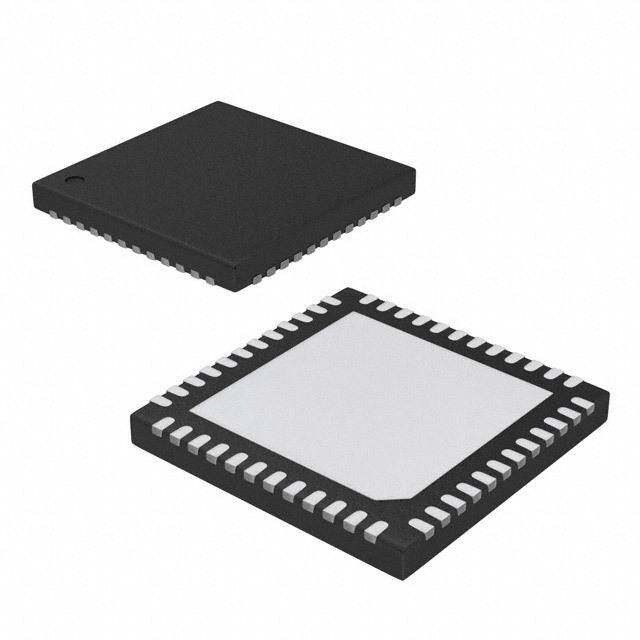
| 描述 | IC LED DRVR BCKLGHT LDO 30WLCSP |
| 产品分类 | |
| 品牌 | Skyworks Solutions Inc |
| 数据手册 | |
| 产品图片 | |
| 产品型号 | AAT2870IUW-T1 |
| rohs | 无铅 / 符合限制有害物质指令(RoHS)规范要求 |
| 产品系列 | - |
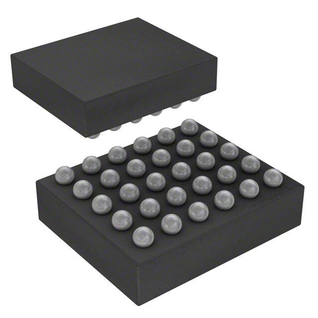
| 供应商器件封装 | 30-WLCSP (3.1x2.6) |
| 其它名称 | 863-1473-6 |
| 内部驱动器 | 是 |
| 包装 | Digi-Reel® |
| 安装类型 | 表面贴装 |
| 封装/外壳 | 30-WFBGA,WLCSP |
| 工作温度 | -40°C ~ 85°C |
| 恒压 | - |
| 恒流 | 是 |
| 拓扑 | 线性(LDO),PWM,切换式电容器(充电泵) |
| 标准包装 | 1 |
| 电压-电源 | 2.7 V ~ 5.5 V |
| 电压-输出 | - |
| 类型-初级 | 背光,照明管理装置(LMU) |
| 类型-次级 | RGB,白色 LED |
| 输出数 | 12 |
| 频率 | 1.17MHz ~ 1.43MHz |


- 商务部:美国ITC正式对集成电路等产品启动337调查
- 曝三星4nm工艺存在良率问题 高通将骁龙8 Gen1或转产台积电
- 太阳诱电将投资9.5亿元在常州建新厂生产MLCC 预计2023年完工
- 英特尔发布欧洲新工厂建设计划 深化IDM 2.0 战略
- 台积电先进制程称霸业界 有大客户加持明年业绩稳了
- 达到5530亿美元!SIA预计今年全球半导体销售额将创下新高
- 英特尔拟将自动驾驶子公司Mobileye上市 估值或超500亿美元
- 三星加码芯片和SET,合并消费电子和移动部门,撤换高东真等 CEO
- 三星电子宣布重大人事变动 还合并消费电子和移动部门
- 海关总署:前11个月进口集成电路产品价值2.52万亿元 增长14.8%


PDF Datasheet 数据手册内容提取
DATA SHEET AAT2870 LED Backlight Driver and Multiple LDO Lighting Management Unit General Description Features The AAT2870 is a highly integrated charge pump-based • Charge Pump Input Voltage Range: 2.7V to 5.5V lighting management unit (LMU) providing eight inde- • Tri-Mode Negative Charge Pump pendently configurable LED channels that can also be ▪ Improved Efficiency grouped into main or sub backlight controls. The built-in ▪ Drives up to Eight LEDs support for low cost ambient light sensors automates all • 1.3MHz Switching Frequency brightness adjustments. In addition, four programmable • Automatic Soft Start low dropout (LDO) linear regulators are provided to sup- • Industry Standard I2C Programming Interface ply other lighting and camera module functions. The LMU • Programmable Backlight Current (8 Channels) is optimized for single-cell lithium-ion/polymer systems ▪ 27.9mA Maximum Current per Channel making it ideal for portable devices. ▪ 32 Levels (5 bits): 0.45mA – 27.9mA ▪ Independent Main or Sub Settings A tri-mode negative charge pump provides power to ▪ Programmable Fade-On / Off backlight LEDs with improved efficiency over conven- • Advanced Dimming Features: tional charge pump topologies. All eight backlight LED ▪ Ambient Light Sensor Management current sinks are programmable up to 27.9mA. LEDs ▪ Direct Ambient Dimming Function may be set individually or in groups for various arrays of • 128 Programmable Levels backlight or keypad lighting applications. High frequency ▪ PWM Dimming (CABC Compatible) PWM dimming for both Main and Sub display backlight- • Four Linear Regulators ing is provided and is compliant to Content Adaptive ▪ LDOA up to 300mA Brightness Control (CABC) specifications with a PWM ▪ LDOB, C and D up to 150mA frequency up to 100 kHz. ▪ 150mV Dropout The ambient light control features automatic sensor ▪ I2C Programmable Outputs: 1.2V to 3.3V calibration and 50Hz/60Hz noise rejection for accurate ▪ Output Auto-Discharge for Fast Shutdown brightness adjustment without processor intervention. • Built-In Over-Temperature Protection • -40°C to +85°C Temperature Range All AAT2870 functions are programmed using an industry • 3.1mm x 2.6mm, 0.5mm ball pitch, 30 ball standard bi-directional I2C interface. This interface can CSP package enable, disable, and set the backlight current to one of 32 levels (5 bits) for the backlight. Backlight current matching is better than ±3% for uniform display/sub- Applications display brightness. • Camera Enabled Mobile Devices The AAT2870 also contains four high-performance low- • Digital Still Cameras noise, low dropout (LDO) linear regulators. Each regulator • Smart Phones starts up with a default 1.2V and is adjustable by pro- gramming through the I2C interface. LDOA can supply up to 300mA, while LDOB, C and D can source up to 150mA to a system load. The AAT2870 is available in a Pb-free, space-saving 3.1mm x 2.6mm, 30 ball CSP package rated over the -40°C to +85°C temperature range. Skyworks Solutions, Inc. • Phone [781] 376-3000 • Fax [781] 376-3100 • sales@skyworksinc.com • www.skyworksinc.com 1 202074A • Skyworks Proprietary Information • Products and Product Information are Subject to Change Without Notice. • June 15, 2012
DATA SHEET AAT2870 LED Backlight Driver and Multiple LDO Lighting Management Unit Typical Application C 1 C 1 1 2 0.22μF 0.22μF C NEG V 2 .2 μ F IN V IN C 1+ C 1 - C 2+ C 2 - Backlight IN NEG IN_ LDO V BAT CIN 3.6V 2.2μF AAT2870 BL1 Enable EN BL2 BL3 I2C Data Input SDA BL4 I2C Clock Input SCL BL5 BL6 PWM Control Input BC_M BL7 BL8 CF 10nF FLTR C 2.2μF SBIAS SBIAS V LDOA LDOA 300mA V LDOB 15LD0OmBA CLDOA 4.7μF AMB_IN External Ambien t C LDOB Light Sensor 2.2μF (Photo Diode or Transistor) V LDOC LDOC 150mA V LDOD LDOD 150mA AGND PGND C LDOC C LDOD 2.2μF 2.2μF 1. Or alternate value of 1μF. Skyworks Solutions, Inc. • Phone [781] 376-3000 • Fax [781] 376-3100 • sales@skyworksinc.com • www.skyworksinc.com 2 202074A • Skyworks Proprietary Information • Products and Product Information are Subject to Change Without Notice. • June 15, 2012
DATA SHEET AAT2870 LED Backlight Driver and Multiple LDO Lighting Management Unit Pin Descriptions Ball # Symbol Description LDOA regulated voltage output pin. Bypass LDOA to AGND with a 4.7μF or larger ceramic capacitor as close A1 LDOA to the AAT2870 as possible. LDOD regulated voltage output pin. Bypass LDOD to AGND with a 2.2μF or larger ceramic capacitor as close A2 LDOD to the AAT2870 as possible. A3 AGND Analog ground. Connect AGND to PGND at a single point as close to the AAT2870 as possible. A4 IN_LDO Input power supply pin for all four LDO voltage regulators. Must be externally connected to IN. Power input that is internally connected to IN_LDO. Connect IN to the input source voltage and bypass to A5 IN PGND with a 2.2μF or larger ceramic capacitor as close to the AAT2870 as possible. Connect LED anodes to IN. LDOB regulated voltage output pin. Bypass LDOB to AGND with a 2.2μF or larger ceramic capacitor as close B1 LDOB to the AAT2870 as possible. LDOC regulated voltage output pin. Bypass LDOC to AGND with a 2.2μF or larger ceramic capacitor as close B2 LDOC to the AAT2870 as possible. Ambient light sensor bias supply output. This pin provides a regulated bias supply to the attached ambi- B3 SBIAS ent light sensor. Refer to "Ambient Light Sensor Voltage Bias" in the Application Information section of this datasheet for more details. B4 C1+ Positive terminal of charge pump capacitor 1. Connect the 0.22μF1 charge pump capacitor 1 from C1+ to C1-. B5 C2+ Positive terminal of charge pump capacitor 2. Connect the 0.22μF1 charge pump capacitor 2 from C2+ to C2-. Ambient light sensor input connection pin. Connect the photo diode anode or ambient light sensor module C1 AMB_IN output to this pin. C2 FLTR BC_M PWM input fi lter capacitor pin. Connect a 10nF ceramic capacitor between this pin and AGND. C3 SDA I2C serial data pin. This pin is bi-directional. C4 C2- Negative terminal of charge pump capacitor 2. C5 PGND Power ground. Connect AGND to PGND at a single point as close to the AAT2870 as possible. Content adjustable brightness control PWM signal input. Refer to "Content Adjustable Brightness Control" in D1 BC_M the Application Information section of this datasheet for more details. D2 EN Enable pin. Drive high to enable, low to shutdown. D3 SCL I2C serial clock input pin D4 C1- Negative terminal of charge pump capacitor 1. Charge pump output. NEG is the output of the charge pump and supplies current to the backlight LEDs. D5 NEG Bypass NEG to IN with a 2.2μF or larger ceramic capacitor located as close to the AAT2870 as possible. E1 AGND Analog ground. Connect AGND to PGND at a single point as close to the AAT2870 as possible. Backlight LED 7 current sink. BL7 controls the current through backlight LED 7. Connect the cathode of E2 BL7 backlight LED 7 to BL7. If not used, connect BL7 to IN. Backlight LED 5 current sink. BL5 controls the current through backlight LED 5. Connect the cathode of E3 BL5 backlight LED 5 to BL5. If not used, connect BL5 to IN. Backlight LED 4 current sink. BL4 controls the current through backlight LED 4. Connect the cathode of E4 BL4 backlight LED 4 to BL4. If not used, connect BL4 to IN. Backlight LED 2 current sink. BL2 controls the current through backlight LED 2. Connect the cathode of E5 BL2 backlight LED 2 to BL2. If not used, connect BL2 to IN. Backlight LED 8 current sink. BL8 controls the current through backlight LED 8. Connect the cathode of F1 BL8 backlight LED 8 to BL8. If not used, connect BL8 to IN. Backlight LED 6 current sink. BL6 controls the current through backlight LED 6. Connect the cathode of F2 BL6 backlight LED 6 to BL6. If not used, connect BL6 to IN. F3 PGND Power ground. Connect AGND to PGND at a single point as close to the AAT2870 as possible. Backlight LED 3 current sink. BL3 controls the current through backlight LED 3. Connect the cathode of F4 BL3 backlight LED 3 to BL3. If not used, connect BL3 to IN. Backlight LED 1 current sink. BL1 controls the current through backlight LED 1. Connect the cathode of F5 BL1 backlight LED 1 to BL1. If not used, connect BL1 to IN. 1. Or alternate value of 1μF. Skyworks Solutions, Inc. • Phone [781] 376-3000 • Fax [781] 376-3100 • sales@skyworksinc.com • www.skyworksinc.com 3 202074A • Skyworks Proprietary Information • Products and Product Information are Subject to Change Without Notice. • June 15, 2012
DATA SHEET AAT2870 LED Backlight Driver and Multiple LDO Lighting Management Unit Pin Configuration WLCSP-30 3.1mm x 2.6mm, 6x5 ball array CSP package (Top View) 3.1 mm A5 B5 C5 D5 E5 F5 5 A4 B4 C4 D4 E4 F4 4 m m A3 B3 C3 D3 E3 F3 3 6 2. A2 B2 C2 D2 E2 F2 2 A1 B1 C1 D1 E1 F1 1 A B C D E F Absolute Maximum Ratings1 Symbol Description Value Units IN to AGND, PGND -0.3 to 6.0 BL1, BL2, BL3, BL4, BL5, BL6, BL7, BL8 to AGND, PGND V -0.3 to V + 0.3 NEG IN NEG to AGND, PGND V – 6.0 to 0.3 IN V C1-, C2- to AGND, PGND V – 6.0 to 0.3 IN LDOA, LDOB, LDOC, LDOD, SDA, SCL, FLTR, C1+, C2+ to AGND, PGND -0.3 to V + 0.3 IN V Ambient Light Sensor Maximum Input Voltage V ALS(MAX) IN Thermal Information Symbol Description Value Units Thermal Resistance2 67 °C/W JA P Maximum Power Dissipation2, 3 1.5 W D T Operating Temperature Range -40 to 85 A T Junction Temperature Range -40 to 150 °C J T Maximum Soldering Temperature (at leads, 10 sec.) 300 LEAD 1. Stresses above those listed in Absolute Maximum Ratings may cause permanent damage to the device. Functional operation at conditions other than the operating conditions specified is not implied. 2. Mounted on an FR4 board. 3. Derate 15mW/°C above 25°C. Skyworks Solutions, Inc. • Phone [781] 376-3000 • Fax [781] 376-3100 • sales@skyworksinc.com • www.skyworksinc.com 4 202074A • Skyworks Proprietary Information • Products and Product Information are Subject to Change Without Notice. • June 15, 2012
DATA SHEET AAT2870 LED Backlight Driver and Multiple LDO Lighting Management Unit Electrical Characteristics1 V = 3.6V; C = C = 0.22μF; C = C = C = C = 2.2μF; C = 4.7μF; T = -40°C to 85°C unless oth- IN 1 2 IN NEG LDO[B,C,D] SBIAS LDO[A] A erwise noted. Typical values are at T = 25°C. A Symbol Description Conditions Min Typ Max Units Charge Pump Input Operating V 2.7 5.5 V IN Voltage Range BL1-BL8=OFF; LDO[A,B,C,D] = OFF via I2C 600 μA 1x mode, LDO[A,B,C,D] = OFF; BL1-BL8 = OFF via I2C 2 mA 1.5x mode; LDO[A,B,C,D] = OFF via I2C; BL1-BL8 = OPEN 4 6.0 mA I IN Operating Current IN 2x mode; LDO[A,B,C,D] = OFF via I2C; BL1-BL8 = OPEN 4 mA LDO[A,B,C,D] = ON via I2C; No Load 250 μA LDOA = ON; LDO[B,C,D] = OFF via I2C; No Load 155 μA I IN Shutdown Current LDO[A,B,C,D] = OFF via I2C 1.0 μA IN(SHDN) Over-Temperature Shutdown T 140 °C SD Threshold Over-Temperature Shutdown T 15 °C SD(HYS) Hysteresis Charge Pump Section V NEG Output Voltage V - V 5.0 V NEG IN NEG BL1-BL8 Charge Pump Mode V 1.5x to 1x Mode Transition 0.3 V IN(TH_H, BL) Transition Hysteresis Charge Pump Oscillator f T = 25°C 1.17 1.3 1.43 MHz OSC Frequency A t Charge Pump Soft-start Time 100 μs CP(SS) BL1-BL8 LED Drivers V – V = 1V 18 19.8 22 mA I BL1-BL8 Current Accuracy IN F BLx V – V = 1V 1.44 1.8 2.16 mA IN F ΔI / (BLx) BL1-BL8 Current Matching2 V – V = 1V 3 % I IN F BL(AVG) BL1-BL8 Charge Pump V 100 mV BL_(TH) Transition Threshold BL1-BL8 Automatic Fade In/ t V – V = 1V 0.75 1 1.25 s FADE Out Timer3 IN F 1. The AAT2870 is guaranteed to meet performance specifications over the -40°C to +85°C operating temperature range and is assured by design, characterization, and correla- tion with statistical process controls. 2. Current matching is defined as the deviation of any sink current from the average of all channels. 3. Guaranteed by fOSC. Skyworks Solutions, Inc. • Phone [781] 376-3000 • Fax [781] 376-3100 • sales@skyworksinc.com • www.skyworksinc.com 5 202074A • Skyworks Proprietary Information • Products and Product Information are Subject to Change Without Notice. • June 15, 2012
DATA SHEET AAT2870 LED Backlight Driver and Multiple LDO Lighting Management Unit Electrical Characteristics1 V = 3.6V; C = C = 0.22μF; C = C = C = C = 2.2μF; C = 4.7μF; T = -40°C to 85°C unless oth- IN 1 2 IN NEG LDO[B,C,D] SBIAS LDO[A] A erwise noted. Typical values are at T = 25°C. A Symbol Description Conditions Min Typ Max Units Linear Regulators V + V LDO Regulators Input Supply OUT 5.5 V IN_LDO V DO ΔVLDO[A/B/C/D]/ LDOA, LDOB, LDOC, LDOD Output ILDO = 1mA to 150mA; TA = 25°C -2.0 2.0 % VLDO[A/B/C/D] Voltage Tolerance ILDO = 1mA to 150mA; TA = -40°C to +85°C -3.0 3.0 % I LDOA Maximum Load Current 300 mA LDO[A](MAX) LDOB, LDOC LDOD Maximum Load I 150 mA LDO[B/C/D](MAX) Current V LDOA Dropout Voltage V ≥ 3.0V; I = 300mA 200 mV LDO[A](DO) LDO[A] OUT V LDOB, LDOC, LDOD Dropout Voltage2 V ≥ 3.0V; I = 150mA 150 mV LDO[B/C/D](DO) LDO[B/C/D] OUT ∆V / LDOA, LDOB, LDOC, LDOD LDO V = (V + 1V) to 5V 0.09 %/V V *∆V Line Regulation IN LDO[A/B/C/D] LDO IN LDOA, LDOB, LDOC, LDOD Power PSRR I = 10mA, 1kHz 50 dB [A/B/C/D] Supply Rejection Ratio LDO[A/B/C/D] LDOA, LDOB, LDOC, LDOD Auto- R 1 kΩ LDO_(DCHG) Discharge Resistance Ambient Light Sensor Interface V Ambient Light Sensor Bias Voltage VSBIAS = 3.0V, ISBIAS = 200μA 2.85 3.0 3.15 V SBIAS Output Tolerance V = 2.6V, I = 200μA 2.47 2.60 2.73 SBIAS SBIAS I SBIAS Maximum Output Current 30 mA OUT(SBIAS)[MAX] Ambient Light Sensor Maximum V 1.6 V ALS(MAX) Input Voltage ALS ADC Maximum Input Leakage I 1 μA IN(ALS)[MAX] Current R SBIAS Auto-Discharge Resistance 1 kΩ OUT(SBIAS)[DCHG] Input Threshold Levels – EN, BC_M V Input Low Threshold 0.4 V TH(L) V Input High Threshold 1.4 V TH(H) I2C Logic and Control Interface V SDA, SCL Input Low Threshold 2.7V ≤ V ≤ 5.5V 0.4 V IL IN V SDA, SCL Input High Threshold 2.7V ≤ V ≤ 5.5V 1.4 V IH IN V SDA Output Low Voltage I = 3mA 0.4 V OL PULL-UP I SDA, SCL, EN Input Leakage Current V = V = V = 5V -1 1 μA IN SDA SCL EN f SCL Clock Frequency 0 400 kHz SCL t SCL Clock Low Period 1.3 μs LOW t SCL Clock High Period 0.6 μs HIGH t Hold Time START Condition 0.6 μs HD_STA t SDA Data Setup Time 100 ns SU_DAT t SDA Data HOLD Time 0 0.9 μs HD_DAT t Setup Time for STOP Condition 0.6 μs SU_STO Bus Free Time Between STOP and t 1.3 μs BUF START Conditions 1. The AAT2870 is guaranteed to meet performance specifications over the -40°C to +85°C operating temperature range and is assured by design, characterization, and correla- tion with statistical process controls. 2. VLDO[A/B/C/D][DO] is defined as VIN – VLDO[A/B/C/D] when VLDO[A/B/C/D] is 98% of nominal. Skyworks Solutions, Inc. • Phone [781] 376-3000 • Fax [781] 376-3100 • sales@skyworksinc.com • www.skyworksinc.com 6 202074A • Skyworks Proprietary Information • Products and Product Information are Subject to Change Without Notice. • June 15, 2012
DATA SHEET AAT2870 LED Backlight Driver and Multiple LDO Lighting Management Unit Typical Characteristics Input Operating Current, 1x Mode Input Operating Current, 1.5x Mode (V = 3.6V; LDOA/B/C/D = OFF; BL1-BL8 = OFF) (V = 3.6V; LDOA/B/C/D = OFF; BL1-BL8 = OPEN) IN IN 185 2.44 180 2.43 µA) 175 mA) 2.42 nt ( 170 nt ( 2.41 e e urr 165 urr 2.40 C 160 C 2.39 put 155 put 2.38 n n I 150 I 2.37 145 2.36 -40 -15 10 35 60 85 -40 -15 10 35 60 85 Temperature (°C) Temperature (°C) Input Operating Current, 2x Mode Input Operating Current, All LDOs (V = 3.6V; LDOA/B/C/D = OFF; BL1-BL8 = OPEN) (V = 3.6V; V = 1.2V; BL1-BL8 = OFF) IN IN LDOA/B/C/D 2.95 290 2.90 285 mA) 2.85 µA) 280 nt ( 2.80 nt ( 275 e e urr 2.75 urr 270 C 2.70 C 265 put 2.65 put 260 n n I 2.60 I 255 2.55 250 -40 -15 10 35 60 85 -40 -15 10 35 60 85 Temperature (°C) Temperature (°C) Input Operating Current, Single LDO Shutdown Current vs. Temperature (V = 3.6V; V = 1.2V; LDOB/C/D = OFF; BL1-BL8 = OFF) (V = 3.6V; EN = GND) IN LDOA IN 210 400 205 A) 350 nt (µA) 129050 rent (n 320500 e ur rr 190 C 200 ut Cu 185 own 150 p 180 d 100 n ut I 175 h 50 S 170 0 -40 -15 10 35 60 85 -40 -15 10 35 60 85 Temperature (°C) Temperature (°C) Skyworks Solutions, Inc. • Phone [781] 376-3000 • Fax [781] 376-3100 • sales@skyworksinc.com • www.skyworksinc.com 7 202074A • Skyworks Proprietary Information • Products and Product Information are Subject to Change Without Notice. • June 15, 2012
DATA SHEET AAT2870 LED Backlight Driver and Multiple LDO Lighting Management Unit Typical Characteristics Oscillator Frequency Accuracy SBIAS Output Voltage Accuracy vs. Temperature uracy (%) 1.25 (VINv =s .3 .T6Ve;m FpOSeC r=a 1tu.3rMeHz) uracy (%) 00..68 (VIN = 3.6V; ISBIAS = 200µA) Acc 1 Acc 0.4 Oscillator Frequency --010--...215505-40 -15 10 35 60 85 SBIAS Output Voltage ----000000......026482-40 -15 10 35 60 3222....0876VVVV 85 Temperature (°C) Temperature (°C) EN, BC_M, SDA, SCL Input Voltage EN, BC_M, SDA, SCL Input Voltage Threshold High vs. Input Voltage Threshold Low vs. Input Voltage 1.4 1.4 CLh (V) 1.3 CLw (V) 1.3 DA, Sd Hig 11..01 DA, Sd Lo 11..10 M, Sshol 0.8 M, Sshol 0.8 C_hre 0.7 C_hre 0.7 N, But T 0.5 -2450°°CC N, But T 0.5 -2450°°CC Ep 0.4 Ep 0.4 n 85°C n 85°C I 0.2 I 0.2 2.7 3.1 3.5 3.9 4.3 4.7 5.1 5.5 2.7 3.1 3.5 3.9 4.3 4.7 5.1 5.5 Input Voltage (V) Input Voltage (V) Skyworks Solutions, Inc. • Phone [781] 376-3000 • Fax [781] 376-3100 • sales@skyworksinc.com • www.skyworksinc.com 8 202074A • Skyworks Proprietary Information • Products and Product Information are Subject to Change Without Notice. • June 15, 2012
DATA SHEET AAT2870 LED Backlight Driver and Multiple LDO Lighting Management Unit Typical Characteristics Backlight Efficiency vs. Input Voltage Backlight Efficiency vs. Input Voltage (Matched LED Forward Voltages) (Mismatched LED Forward Voltages) 100 100 %) 90 %) 90 y ( 80 y ( 80 c c n n e 70 e 70 ci ci Effi 60 Effi 60 ht 50 ht 50 Backlig 234000 2114795.5...983mmmmAAAA/c///hccchhh, V,,, VVVF FFF= === 2 .3339...V537VV4V Backlig 234000 11495.5..83mmmAAA/c//hcchh, V,, VVF(2FF-((822)-- 88=)) == 3 .334..731V32VV, V,, VVF(1FF)(( 11=)) == 3 33.9..731VVV 2.7 3.1 3.5 3.9 4.3 4.7 5.1 5.5 2.7 3.1 3.5 3.9 4.3 4.7 5.1 5.5 Input Voltage (V) Input Voltage (V) Backlight Current Accuracy vs. Temperature Backlight Current Matching vs. Temperature (I = 19.8mA/ch) (I = 19.8mA/ch) BLX BLX %) 4.0 %) 4.0 y ( 3.0 g ( 3.5 c n ura 2.0 chi 3.0 Acc 1.0 Mat 2.5 nt 0.0 nt 2.0 e e urr -1.0 urr 1.5 C Ch1 Ch5 C ht -2.0 Ch2 Ch6 ht 1.0 klig -3.0 CChh34 CChh78 klig 0.5 c c a -4.0 a 0.0 B -40 -15 10 35 60 85 B -40 -15 10 35 60 85 Temperature (°C) Temperature (°C) Total Backlight Current vs. BC_M Duty Cycle (V = 3.6V; I = 19.8mA/Ch) IN BLX A) 180 m 160 nt ( 140 e rr 120 u C 100 ht 80 g kli 60 c a 40 120kHz B 60kHz al 20 20kHz ot 0 T 0 10 20 30 40 50 60 70 80 90 100 BC_M Duty Cycle (%) Skyworks Solutions, Inc. • Phone [781] 376-3000 • Fax [781] 376-3100 • sales@skyworksinc.com • www.skyworksinc.com 9 202074A • Skyworks Proprietary Information • Products and Product Information are Subject to Change Without Notice. • June 15, 2012
DATA SHEET AAT2870 LED Backlight Driver and Multiple LDO Lighting Management Unit Typical Characteristics LDOA/B/C/D Output Voltage Accuracy LDOA/B/C/D Output Voltage Accuracy vs. Temperature vs. Temperature (V = 3.6V; V = 1.2V; I = 100µA) (V = 3.6V; V = 3.3V; I = 100µA) IN LDOA/B/C/D LDOA/B/C/D IN LDOA/B/C/D LDOA/B/C/D 0.8 0.8 ut%) 0.6 ut%) 0.6 utpcy ( 0.4 utpcy ( 0.4 Oa Oa D ur 0.2 D ur 0.2 C/cc 0 C/cc 0 A/B/ge A-0.2 LDOA A/B/ge A-0.2 LDOA Oa-0.4 LDOB Oa-0.4 LDOB LDVolt-0.6 LDOC LDVolt-0.6 LDOC LDOD LDOD -0.8 -0.8 -40 -15 10 35 60 85 -40 -15 10 35 60 85 Temperature (°C) Temperature (°C) LDOA Output Voltage Load Regulation LDOB/C/D Output Voltage Load Regulation (V = 3.6V; V = 1.2V) (V = 3.6V; V = 1.2V) IN LDOA IN LDOB/C/D 2.0 2.0 e put Voltageulation (%) 0011....0505 utput Voltagulation (%) 0011....0505 OutReg -0.5 D OReg -0.5 LDOA Load --11..50 DOB/C/Load --11..50 LLLDDDOOOBCD -2.0 L -2.0 0.1 1 10 100 1000 0.1 1 10 100 1000 Load Current (mA) Load Current (mA) LDOA Output Voltage Load Regulation LDOB/C/D Output Voltage Load Regulation (V = 3.6V; V = 3.3V) (V = 3.6V; V = 3.3V) IN LDOA IN LDOB/C/D 2.0 2.0 e put Voltageulation (%) 0011....0505 utput Voltagulation (%) 0011....0505 OutReg -0.5 D OReg -0.5 LDOA Load --11..50 DOB/C/Load --11..50 LLLDDDOOOBCD -2.0 L -2.0 0.1 1 10 100 1000 0.1 1 10 100 1000 Load Current (mA) Load Current (mA) Skyworks Solutions, Inc. • Phone [781] 376-3000 • Fax [781] 376-3100 • sales@skyworksinc.com • www.skyworksinc.com 10 202074A • Skyworks Proprietary Information • Products and Product Information are Subject to Change Without Notice. • June 15, 2012
DATA SHEET AAT2870 LED Backlight Driver and Multiple LDO Lighting Management Unit Typical Characteristics LDOA Output Voltage Line Regulation LDOB/C/D Output Voltage Line Regulation (V = 1.2V; I = 20mA) (V = 1.2V; I = 10mA) LDOA LDOA LDOB/C/D LDOB/C/D 0.4 0.4 e put Voltageulation (%) 0000....0312 utput Voltagulation (%) 0000....0312 utg Og ORe -0.1 D Re -0.1 OA ne -0.2 B/C/ne -0.2 LDOB LDLi -0.3 DOLi -0.3 LLDDOOCD -0.4 L -0.4 2.7 3.1 3.5 3.9 4.3 4.7 5.1 5.5 2.7 3.1 3.5 3.9 4.3 4.7 5.1 5.5 Input Voltage (V) Input Voltage (V) LDOA Output Voltage Line Regulation LDOB/C/D Output Voltage Line Regulation (V = 3.3V; I = 20mA) (V = 3.3V; I = 10mA) LDOA LDOA LDOB/C/D LDOB/C/D 0.4 0.4 e put Voltageulation (%) 0000....0312 utput Voltagulation (%) 0000....0312 utg Og ORe -0.1 D Re -0.1 OA ne -0.2 B/C/ne -0.2 LDOB LDLi -0.3 DOLi -0.3 LLDDOOCD -0.4 L -0.4 3.4 3.7 4.0 4.3 4.6 4.9 5.2 5.5 3.4 3.7 4.0 4.3 4.6 4.9 5.2 5.5 Input Voltage (V) Input Voltage (V) Backlight Turn ON Characteristics, 1x Mode Backlight Turn ON Characteristics, 1.5x Mode (V = 4.2V; I = 19.8mA/ch) (V = 3.6V; I = 19.8mA/ch) IN BLX IN BLX V V SDA SDA (2V/div) (2V/div) 0V 0V V V NEG NEG (2V/div) 0V (2V/div) 0V VSINK VSINK (2V/div) 0V (2V/div) 0V I IN (200mA/div) 0A IIN (200mA/div) 0A Time (100µs/div) Time (100µs/div) Skyworks Solutions, Inc. • Phone [781] 376-3000 • Fax [781] 376-3100 • sales@skyworksinc.com • www.skyworksinc.com 11 202074A • Skyworks Proprietary Information • Products and Product Information are Subject to Change Without Notice. • June 15, 2012
DATA SHEET AAT2870 LED Backlight Driver and Multiple LDO Lighting Management Unit Typical Characteristics Backlight Turn ON Characteristics, 2x Mode Backlight Turn OFF Characteristics, 1.5x Mode (V = 3.0V; I = 19.8mA/ch) (V = 3.6V; I = 19.8mA/ch) IN BLX IN BLX V V SDA SDA (2V/div) (2V/div) 0V 0V V V (2V/dNiEvG) 0V (2V/dNiEvG) 0V V V SINK SINK (2V/div) 0V (2V/div) 0V I I 0A IN IN (200mA/div) 0A (200mA/div) Time (100µs/div) Time (100µs/div) Backlight Operating Characteristics, 1.5X Mode Backlight Operating Characteristics, 2x Mode (V = 3.6V; I = 19.8mA/ch) (V = 2.9; I = 19.8mA/ch) IN BLX IN BLX V V IN IN (50mV/div) (50mV/div) (AC Coupled) (AC Coupled) V V NEG NEG (100mV/div) (100mV/div) (AC Coupled) (AC Coupled) V V SINK SINK (100mV/div) (50mV/div) (AC Coupled) (AC Coupled) I I IN IN (10mA/div) (10mA/div) (AC Coupled) (AC Coupled) Time (200ns/div) Time (200ns/div) LDOA Line Transient LDOB/C/D Line Transient (V = 3.6V-4.2V; V = 1.2V; I = 20mA) (V = 3.6V-4.2V; V = 1.2V; I = 10mA) IN LDOA LDOA IN LDOB/C/D LDOB/C/D V V IN IN (500mV/div) (500mV/div) (AC Coupled) (AC Coupled) V V LDOA LDOB/C/D (10mV/div) (10mV/div) (AC Coupled) (AC Coupled) Time (200µs/div) Time (200µs/div) Skyworks Solutions, Inc. • Phone [781] 376-3000 • Fax [781] 376-3100 • sales@skyworksinc.com • www.skyworksinc.com 12 202074A • Skyworks Proprietary Information • Products and Product Information are Subject to Change Without Notice. • June 15, 2012
DATA SHEET AAT2870 LED Backlight Driver and Multiple LDO Lighting Management Unit Typical Characteristics LDOA Line Transient LDOB/C/D Line Transient (V = 3.6V-4.2V; V = 3.3V; I = 20mA) (V = 3.6V-4.2V; V = 3.3V; I = 10mA) IN LDOA LDOA IN LDOB/C/D LDOB/C/D V V IN IN (500mV/div) (500mV/div) (AC Coupled) (AC Coupled) V V LDOA LDOB/C/D (10mV/div) (10mV/div) (AC Coupled) (AC Coupled) Time (200µs/div) Time (200µs/div) LDOA Load Transient LDOB/C/D Load Transient (V = 3.6V; V = 1.2V; I = 10mA-200mA) (V = 3.6V; V = 1.2V; I = 10mA-100mA) IN LDOA LDOA IN LDOB/C/D LDOB/C/D I I LDOA LDOB/C/D (100mA/div) (50mA/div) V V LDOA LDOB/C/D (50mV/div) (20mV/div) (AC Coupled) (AC Coupled) Time (5µs/div) Time (5µs/div) LDOA Load Transient LDOB/C/D Load Transient (V = 3.6V; V = 3.3V; I = 10mA-200mA) (V = 3.6V; V = 3.3V; I = 10mA-100mA) IN LDOA LDOA IN LDOB/C/D LDOB/C/D I I LDOA LDOB/C/D (100mA/div) (50mA/div) V V LDOA LDOB/C/D (50mV/div) (50mV/div) (AC Coupled) (AC Coupled) Time (20µs/div) Time (20µs/div) Skyworks Solutions, Inc. • Phone [781] 376-3000 • Fax [781] 376-3100 • sales@skyworksinc.com • www.skyworksinc.com 13 202074A • Skyworks Proprietary Information • Products and Product Information are Subject to Change Without Notice. • June 15, 2012
DATA SHEET AAT2870 LED Backlight Driver and Multiple LDO Lighting Management Unit Functional Block Diagram NEG C1+ 1x/1.5x/2x C1- Tri-mode Negative BL1 C2+ Charge Pump C2- BL2 BL3 SBIAS LDO Regulato r Backligh t BL4 Current 8 AMB_IN Programm ab le Control BL5 Amplifier+ADC BL6 BL7 BL8 EN BC_M Contro l FLTR Logic LDO A LDOA 300mA LDOB LDOB 150mA SDA I2C Interface SCL REF LDOC LDOC 150mA Over-Temper ature Monitor IN LDO D LDOD 150mA IN _ LDO AGND PGND Skyworks Solutions, Inc. • Phone [781] 376-3000 • Fax [781] 376-3100 • sales@skyworksinc.com • www.skyworksinc.com 14 202074A • Skyworks Proprietary Information • Products and Product Information are Subject to Change Without Notice. • June 15, 2012
DATA SHEET AAT2870 LED Backlight Driver and Multiple LDO Lighting Management Unit Functional Description input and LED forward voltages while maintaining high efficiency. The AAT2870 is a highly integrated display backlight, The charge pump is controlled by the voltage across the keypad and auxiliary LED driver with four LDO regulators LED current sinks when programmed for a desired con- to power system functions. A negative charge pump stant current. When any one of the active backlight cur- delivers improved power conversion efficiency over con- rent sink channels drop below the transition threshold, ventional charge pump devices and drives backlight the charge pump goes to the next higher operating LEDs from a 2.7V to 5.5V input voltage source. The mode (from 1x to 1.5x or from 1.5x to 2x mode) to AAT2870 may be configured to drive any combination of maintain sufficient LED voltage for a given constant LED 8 backlight LEDs either individually or in any desired current. AAT2870 continuously monitors the LED for- grouping. The AAT2870 is compatible with CABC sys- ward voltages and uses the input voltage to determine tems by providing a filtered PWM input for external when to reduce the charge pump operating mode for brightness adjustment based on display content or better efficiency. There is also a mode-transition hyster- ambient light conditions. The regulated bias supply out- esis to maintain charge pump stability between modes. put supports ambient light sensors and photo diodes. The integrated ADC polls the ambient light conditions and is readable through the I2C interface. The ambient LED Current Control light control can also be configured to adjust pro- The backlight LED constant current levels are controlled grammed LED current automatically for changing ambi- through the I2C interface. The backlight LED current can ent lighting conditions. be set between 0.45mA and 27.9mA in approximately In addition to LED backlighting functions, four indepen- 1mA steps. The LED channels may be programmed and dent LDO regulators are provided. The LDO regulators enabled globally, in groups of Main, Sub or individually. produce programmable output voltages between 1.2V Backlight fade-in/out and ambient light control functions and 3.3V. The bi-directional I2C interface provides simple are configured through the I2C interface. See the and easy programming of all LED backlight functions, “Backlight Current Programming” section for more infor- ambient light sensor control and LDO regulator output mation. voltage levels. Ambient Light Sensor Control LED Drivers The AAT2870 ambient light sensor control circuit pro- The AAT2870 drives any combination of eight backlight vides an interface and control of an external ambient LEDs up to 27.9mA each. The LEDs are independently light sensor module or photo diode. The system incorpo- driven by a negative charge pump circuit to ensure that rates a programmable voltage sensor bias supply constant current is maintained for all possible LED for- (SBIAS) which may be configured to output 3.0V, 2.8V, ward current and voltage levels over the specified input 2.7V or 2.6V and may source up to 30mA. The ALS input battery voltage range. The charge pump automatically has a programmable gain amplifier and ADC which switches from 1x, 1.5x, or 2x modes to maintain the stores one of 16 levels to an internal register to reflect programmed LED current while minimizing power loss the current calibrated ambient light level. The stored and maximizing power conversion efficiency. To further light level data may be read through the bi-directional improve efficiency only the channels that reach the drop- I2C interface to relay the ambient light information to the out condition are independently switched to the charge system display driver. The ALS circuit may also be con- pump supply. The charge pump section operates with a figured to directly adjust a preprogrammed backlight high 1.3MHz switching frequency allowing the use of LED brightness level based on current ambient light small external 0.22μF1 ceramic capacitors. By virtue of conditions. The ADC continuously filters out the 50Hz the negative charge pump, LED anodes are connected and 60Hz flicker noise from indoor lighting, eliminating directly to the input power source. The programmed for- the need for a large capacitor at the output pin of the ward current for each LED is controlled through individu- ambient light sensor. To save power and improve system al constant current sinks, allowing for programmable efficiency, the ALC circuit features manual polling and current control with high accuracy over a wide range of automatic polling with programmable polling times. 1. Or alternate value of 1μF. Skyworks Solutions, Inc. • Phone [781] 376-3000 • Fax [781] 376-3100 • sales@skyworksinc.com • www.skyworksinc.com 15 202074A • Skyworks Proprietary Information • Products and Product Information are Subject to Change Without Notice. • June 15, 2012
DATA SHEET AAT2870 LED Backlight Driver and Multiple LDO Lighting Management Unit Under polling control, the SBIAS regulator, ambient light I2C Serial Interface Protocol sensor and ADC circuit are disabled and only enabled for The AAT2870 uses an I2C serial interface to set backlight a short period to sample, read and store the present LED current and LDO on/off and output voltage, as well ambient light value in the ALS data register. as other housekeeping functions. The AAT2870 acts only as a slave device. LDO Regulators The I2C protocol uses two open-drain inputs; SDA (serial The AAT2870 family includes four low dropout (LDO) lin- data line) and SCL (serial clock line). Both inputs require ear regulators. These regulators are powered from the an external pull up resistor, typically to the input voltage. battery and produce a fixed output voltage set through The I2C protocol is bidirectional. The timing diagram in the I2C interface. LDOA is designed to provide load cur- Figure 1 shows the typical I2C interface protocol. rents up to 300mA and LDOB, C and D and intended for loads up to 150mA each. The output voltage of each LDO Devices on the I2C bus can be either master or slave can be set to one of 16 levels between 1.2V and 3.3V. devices. Both master and slave devices can send and The LDO regulators are turned on/off and programmed receive data over the bus, with the difference being that through the I2C interface with a default voltage level of the master device controls all communication on the 1.2V. Additionally, the I2C interface allows the LDO regu- bus. The I2C communications begins by the master mak- lators to be enabled independently for any combination ing a START condition. Next the master transmits the of output voltages. 7-bit device address and a Read/Write bit. Each slave device on the bus has a unique address. The AAT2870's The LDO regulators require a small 2.2μF (LDOB/C/D) 7-bit device address is 0x60. and a 4.7μF (LDOA) ceramic output capacitor for maxi- mized performance and stability. If improved load tran- sient response is required, larger value capacitors can be used without stability degradation. SDA TLOW TSU_DAT THD_STA TBUF SCL T T T HD_STA T T SU_STA SU_STO HD_DAT HIGH Figure 1: I2C Interface Timing Diagram. Skyworks Solutions, Inc. • Phone [781] 376-3000 • Fax [781] 376-3100 • sales@skyworksinc.com • www.skyworksinc.com 16 202074A • Skyworks Proprietary Information • Products and Product Information are Subject to Change Without Notice. • June 15, 2012
DATA SHEET AAT2870 LED Backlight Driver and Multiple LDO Lighting Management Unit START and STOP Conditions tion setup time (t ), by an SDA low-to-high transi- SU_STO tion. The master does not issue an ACK and releases SCL START and STOP conditions are always generated by the and SDA. master. Prior to initiating a START, both the SDA and SCL pins are inactive and are pulled high through external Transferring Data pull-up resistors. As shown in Figure 2, a START condition occurs when the master pulls the SDA line low and, after Addresses and data are sent with the most significant bit the start condition hold time (tHT_STA), the master strobes transmitted first and the least significant bit transmitted the SCL line low. A START condition acts as a signal to all last as shown in Figures 3 and 4. After each address or devices on the bus that the device initiating the START data transmission, the slave device transmits an ACK sequence is active and will be communicating. signal to indicate that it has received the transmission. The ACK signal is generated by the slave after the mas- A STOP condition, as shown in Figure 2, occurs when SCL ter releases the SDA data line by driving SDA low. changes from low to high followed after the STOP condi- START STOP SDA SDA SCL SCL Figure 2: I2C STOP and START Conditions; START: A High “1” to Low “0” Transition on the SDA Line While SCL is High “1” STOP: A Low “0” to High “1” Transition on the SDA Line While SCL is High “1”. SCL 1 2 3 4 5 6 7 8 9 MSB LSB SDA A6 A5 A4 A3 A2 A1 A0 R/W ACK Device Address Figure 3: I2C Address Bit Map; 7-bit Slave Address (A6-A0), 1-bit Read/Write (R/W), 1-bit Acknowledge (ACK). SCL 1 2 3 4 5 6 7 8 9 MSB LSB SDA D7 D6 D5 D4 D3 D2 D1 D0 ACK Register Address / Data Figure 4: I2C Register Address and Data Bit Map; 8-bit Data (D7-D0), 1-bit Acknowledge (ACK). Skyworks Solutions, Inc. • Phone [781] 376-3000 • Fax [781] 376-3100 • sales@skyworksinc.com • www.skyworksinc.com 17 202074A • Skyworks Proprietary Information • Products and Product Information are Subject to Change Without Notice. • June 15, 2012
DATA SHEET AAT2870 LED Backlight Driver and Multiple LDO Lighting Management Unit Writing to Slave Device Fade In/Out Programming When the Read/Write bit is set to 0 and the address trans- The fade in/out function allows main and sub backlight mitted by the master matches the device address, the channels to fade between two programmed current lev- slave device transmits an Acknowledge (ACK) signal to els in a smooth, logarithmic progression. By default, fade indicate that it is ready to receive data. Next, the master in/out is enabled (bits EN_FM, EN_FS, INIT_FM and transmits the 8-bit register address, and the slave device INIT_FS have a default value of 1). transmits an ACK to indicate that it received the register The fade in/out function for Main backlight can be dis- address. Next, the master transmits the 8-bit data word, abled by writing EN_FM=0 in FM (0Ch) register and for and again the slave device transmits an ACK indicating Sub backlight by writing EN_FS=0 in FS (0Dh) register. that it received the data. This process continues until the The fade function can be interrupted by writing the EN_ master is finished writing to the slave device at which FM and/or EN_FS bits to 0 while a fade event is in prog- time the master generates a STOP condition. A typical ress. When this happens, the current in the channels AAT2870 I2C write transmission is shown in Figure 5. will abruptly change to the ceiling value programmed in BLM[4:0] (main channels) or BLS[4:0] (sub channels) Reading from Slave Device registers. When the Read/Write bit is set to 1 and the address The duration of the fade in/out sequences can be pro- transmitted by the master matches the device address, grammed for Main backlight by setting FMT<1:0> in FM the slave device transmits an Acknowledge (ACK) signal (0Ch) register and for Sub backlight by FST<1:0> in FS to indicate that it is ready to receive data. Next, the (0Dh) register. The default fade in/out timing is 1s. slave device transmits the 8-bit data word, the master reads the data byte and transmits an ACK to indicate Fade In Function that it received the byte, and generates a STOP condi- tion. An example of AAT2870 I2C read transmission is At initial start up, all Main and Sub backlight channels shown in Figure 6. will turn on with default value of 19.8mA per channel unless fade in has been specifically programmed. The Serial Programmed Registers lower current (floor) is programmed using FLRM[3:0] bits from FLR register (for main channels) and bits The AAT2870 has thirty-nine registers listed in Table 1: FLRS[3:0] for sub channels. The default is 0.45mA per • Fourteen for Main/Sub backlight enable, control and channel. The higher current (ceiling) is programmed configuration of fade in/out function using bits BLM[4:0] from BLM (01h) register for main • Twenty-two for ambient light sensor control and con- channels and bits BLS[4:0] from BLS (02h) register for figuration sub channels. • Three for LDOs control and configuration Fade in sequence for Main backlight is initiated when INIT_FM is changed from 0 to 1 in FM (0Ch) register and Backlight Current Programming for Sub backlight when INIT_FS is changed from 0 to 1 All eight backlight channels are disabled by default and in FS (0Dh) register. are assigned as Main backlight. They can easily be pro- grammed in different Main and Sub group configurations Fade Out Function by using BLn (03h to 0Ah) registers. The fade out sequence for Main backlight is initiated Each channel needs to be enabled by setting EN_CHn=1 when INIT_FM is changed from 1 to 0 in FM (0Ch) reg- from EN_CHn (00h) register. The default setting is ister and for Sub backlight when INIT_FS is changed 19.8mA per channel. from 1 to 0 in FS (0Dh) register. The floor current will persist until Main/Sub backlight channels are disabled by writing EN_CHn=0 to EN_CHn (00h) register. Skyworks Solutions, Inc. • Phone [781] 376-3000 • Fax [781] 376-3100 • sales@skyworksinc.com • www.skyworksinc.com 18 202074A • Skyworks Proprietary Information • Products and Product Information are Subject to Change Without Notice. • June 15, 2012
DATA SHEET AAT2870 LED Backlight Driver and Multiple LDO Lighting Management Unit start msb Chip Address lsb w ack msb Register Address lsb ack msb Register Data lsb ack stop SCL SDA start AAT28707-Bit Device Address = 0x60 w ack Address = 00h ack Data = 0Ch ack stop First Byte Writes as 0xC0 Figure 5: AAT2870 I2C Write Diagram. start msb Chip Address lsb r ack msb Register Data lsb ack stop SCL SDA start AAT2870 7-Bit Device Address = 0x60 r ack Data= 08h ack stop First Byte Writes as 0xC1 Figure 6: AAT2870 I2C Read Diagram. Skyworks Solutions, Inc. • Phone [781] 376-3000 • Fax [781] 376-3100 • sales@skyworksinc.com • www.skyworksinc.com 19 202074A • Skyworks Proprietary Information • Products and Product Information are Subject to Change Without Notice. • June 15, 2012
DATA SHEET AAT2870 LED Backlight Driver and Multiple LDO Lighting Management Unit REG Register (hex) Name Bit 7 Bit 6 Bit 5 Bit 4 Bit 3 Bit 2 Bit 1 Bit 0 Description 00h EN_CHn EN_CH8 EN_CH7 EN_CH6 EN_CH5 EN_CH4 EN_CH3 EN_CH2 EN_CH1 see Figure 7 01h BLM BLM[4] BLM[3] BLM[2] BLM[1] BLM[0] see Figure 8 02h BLS BLS[4] BLS[3] BLS[2] BLS[1] BLS[0] see Figure 9 03h BL1 MAIN1 SUB1 BL1[4] BL1[3] BL1[2] BL1[1] BL1[0] 04h BL2 MAIN2 SUB2 BL2[4] BL2[3] BL2[2] BL2[1] BL2[0] 05h BL3 MAIN3 SUB3 BL3[4] BL3[3] BL3[2] BL3[1] BL3[0] 06h BL4 MAIN4 SUB4 BL4[4] BL4[3] BL4[2] BL4[1] BL4[0] see Figure 10 07h BL5 MAIN5 SUB5 BL5[4] BL5[3] BL5[2] BL5[1] BL5[0] 08h BL6 MAIN6 SUB6 BL6[4] BL6[3] BL6[2] BL6[1] BL6[0] 09h BL7 MAIN7 SUB7 BL7[4] BL7[3] BL7[2] BL7[1] BL7[0] 0Ah BL8 MAIN8 SUB8 BL8[4] BL8[3] BL8[2] BL8[1] BL8[0] 0Bh FLR FLRM[3] FLRM[2] FLRM[1] FLRM[0] FLRS[3] FLRS[2] FLRS[1] FLRS[0] see Figure 11 0Ch FM FMT[1] FMT[0] EN_FM INIT_FM see Figure 12 0Dh FS FST[1] FST[0] EN_FS INIT_FS see Figure 13 0Eh ALS_CFG0 SNSR ALSOUT RSET[1] RSET[0] GAIN[1] GAIN[0] GM_SEL EN_ALS see Figure 14 0Fh ALS_CFG1 OS_TM OS_ADJ[3] OS_ADJ[2] OS_ADJ[1] OS_ADJ[0] SB[1] SB[0] EN_SBIAS see Figure 15 10h ALS_CFG2 CABC PMODE PTME[1] PTME[0] G_ADJ[3] G_ADJ[2] G_ADJ[1] G_ADJ[0] see Figure 16 11h AMB AMB[4] AMB[3] AMB[2] AMB[1] AMB[0] see Figure 17 12h ALS0 ALS0[6] ALS0[5] ALS0[4] ALS0[3] ALS0[2] ALS0[1] ALS0[0] 13h ALS1 ALS1[6] ALS1[5] ALS1[4] ALS1[3] ALS1[2] ALS1[1] ALS1[0] 14h ALS2 ALS2[6] ALS2[5] ALS2[4] ALS2[3] ALS2[2] ALS2[1] ALS2[0] 15h ALS3 ALS3[6] ALS3[5] ALS3[4] ALS3[3] ALS3[2] ALS3[1] ALS3[0] 16h ALS4 ALS4[6] ALS4[5] ALS4[4] ALS4[3] ALS4[2] ALS4[1] ALS4[0] 17h ALS5 ALS5[6] ALS5[5] ALS5[4] ALS5[3] ALS5[2] ALS5[1] ALS5[0] 18h ALS6 ALS6[6] ALS6[5] ALS6[4] ALS6[3] ALS6[2] ALS6[1] ALS6[0] 19h ALS7 ALS7[6] ALS7[5] ALS7[4] ALS7[3] ALS7[2] ALS7[1] ALS7[0] see Figure 18 1Ah ALS8 ALS8[6] ALS8[5] ALS8[4] ALS8[3] ALS8[2] ALS8[1] ALS8[0] 1Bh ALS9 ALS9[6] ALS9[5] ALS9[4] ALS9[3] ALS9[2] ALS9[1] ALS9[0] 1Ch ALSA ALSA[6] ALSA[5] ALSA[4] ALSA[3] ALSA[2] ALSA[1] ALSA[0] 1Dh ALSB ALSB[6] ALSB[5] ALSB[4] ALSB[3] ALSB[2] ALSB[1] ALSB[0] 1Eh ALSC ALSC[6] ALSC[5] ALSC[4] ALSC[3] ALSC[2] ALSC[1] ALSC[0] 1Fh ALSD ALSD[6] ALSD[5] ALSD[4] ALSD[3] ALSD[2] ALSD[1] ALSD[0] 20h ALSE ALSE[6] ALSE[5] ALSE[4] ALSE[3] ALSE[2] ALSE[1] ALSE[0] 21h ALSF ALSF[6] ALSF[5] ALSF[4] ALSF[3] ALSF[2] ALSF[1] ALSF[0] 22h SUB_SET HIGH[3] HIGH[2] HIGH[1] HIGH[0] LOW[3] LOW[2] LOW[1] LOW[0] see Figure 19 23h SUB_CTRL SUB_RESP EN_SUB see Figure 20 24h LDO_AB LDOA[3] LDOA[2] LDOA[1] LDOA[0] LDOB[3] LDOB[2] LDOB[1] LDOB[0] see Figure 21 25h LDO_CD LDOC[3] LDOC[2] LDOC[1] LDOC[0] LDOD[3] LDOD[2] LDOD[1] LDOD[0] see Figure 22 26h EN_LDO 0 0 0 0 EN_LDOD EN_LDOC EN_LDOB EN_LDOA see Figure 23 Table 1: AAT2870 Configuration/Control Register Allocation. (“0” must write 0; Blank space = unassigned) Skyworks Solutions, Inc. • Phone [781] 376-3000 • Fax [781] 376-3100 • sales@skyworksinc.com • www.skyworksinc.com 20 202074A • Skyworks Proprietary Information • Products and Product Information are Subject to Change Without Notice. • June 15, 2012
DATA SHEET AAT2870 LED Backlight Driver and Multiple LDO Lighting Management Unit Backlight Control Registers EN_CHn: Backlight Channels Enable Register (Address 00h, Default 00h) W-0 W-0 W-0 W-0 W-0 W-0 W-0 W-01 EN_CH8 EN_CH7 EN_CH6 EN_CH5 EN_CH4 EN_CH3 EN_CH2 EN_CH1 Bit 7 Bit 0 Bit 7 – Bit 0 EN_CH<8:1>: Backlight Channels Enable Register 11111111 = All 8 backlight channels are enabled 00000000 = All 8 backlight channels are disabled Legend: R = Readable bit W = Writeable bit U = Unassigned n = Channel number -v = Default value ‘1’ = Bit is set ‘0’ = Bit is cleared x = Bit is unknown 1. W-0 means bit 0 is writeable with default value 0 Figure 7: Backlight Channels Enable Register. Skyworks Solutions, Inc. • Phone [781] 376-3000 • Fax [781] 376-3100 • sales@skyworksinc.com • www.skyworksinc.com 21 202074A • Skyworks Proprietary Information • Products and Product Information are Subject to Change Without Notice. • June 15, 2012
DATA SHEET AAT2870 LED Backlight Driver and Multiple LDO Lighting Management Unit BLM: Main Backlight Control Register BLS: Sub Backlight Control Register (Address 01h, Default 16h) (Address 02h, Default 16h) U-0 U-0 U-0 W-1 W-0 W-1 W-1 W-01 U-0 U-0 U-0 W-1 W-0 W-1 W-1 W-01 -- -- -- BLM[4] BLM[3] BLM[2] BLM[1] BLM[0] -- -- -- BLS[4] BLS[3] BLS[2] BLS[1] BLS[0] Bit 7 Bit 0 Bit 7 Bit 0 Bit 7 – Bit 5 Unassigned Bit 7 – Bit 5 Unassigned Bit 4 – Bit 0 BLM<4:0>:Main Backlight Current Magnitude Bit 4 – Bit 0 BLS<4:0>:Sub Backlight Current Magnitude 00000 = 0.45 mA 00000 = 0.45 mA 00001 = 0.90 mA 00001 = 0.90 mA 00010 = 1.80 mA 00010 = 1.80 mA 00011 = 2.70 mA 00011 = 2.70 mA 00100 = 3.60 mA 00100 = 3.60 mA 00101 = 4.50 mA 00101 = 4.50 mA 00110 = 5.40 mA 00110 = 5.40 mA 00111 = 6.30 mA 00111 = 6.30 mA 01000 = 7.20 mA 01000 = 7.20 mA 01001 = 8.10 mA 01001 = 8.10 mA 01010 = 9.00 mA 01010 = 9.00 mA 01011 = 9.90 mA 01011 = 9.90 mA 01100 = 10.8 mA 01100 = 10.8 mA 01101 = 11.7 mA 01101 = 11.7 mA 01110 = 12.6 mA 01110 = 12.6 mA 01111 = 13.5 mA 01111 = 13.5 mA 10000 = 14.4 mA 10000 = 14.4 mA 10001 = 15.3 mA 10001 = 15.3 mA 10010 = 16.2 mA 10010 = 16.2 mA 10011 = 17.1 mA 10011 = 17.1 mA 10100 = 18.0 mA 10100 = 18.0 mA 10101 = 18.9 mA 10101 = 18.9 mA 10110 = 19.8 mA 10110 = 19.8 mA 10111 = 20.7 mA 10111 = 20.7 mA 11000 = 21.6 mA 11000 = 21.6 mA 11001 = 22.5 mA 11001 = 22.5 mA 11010 = 23.4 mA 11010 = 23.4 mA 11011 = 24.3 mA 11011 = 24.3 mA 11100 = 25.2 mA 11100 = 25.2 mA 11101 = 26.1 mA 11101 = 26.1 mA 11110 = 27.0 mA 11110 = 27.0 mA 11111 = 27.9 mA 11111 = 27.9 mA Legend: Legend: R = Readable bit W = Writeable bit U = Unassigned n = Channel number R = Readable bit W = Writeable bit U = Unassigned n = Channel number -v = Default value ‘1’ = Bit is set ‘0’ = Bit is cleared x = Bit is unknown -v = Default value ‘1’ = Bit is set ‘0’ = Bit is cleared x = Bit is unknown 1. W-0 means bit 0 is writeable with default value 0 1. W-0 means bit 0 is writeable with default value 0 Figure 8: Backlight Main Control Register. Figure 9: Sub Backlight Control Register. Skyworks Solutions, Inc. • Phone [781] 376-3000 • Fax [781] 376-3100 • sales@skyworksinc.com • www.skyworksinc.com 22 202074A • Skyworks Proprietary Information • Products and Product Information are Subject to Change Without Notice. • June 15, 2012
DATA SHEET AAT2870 LED Backlight Driver and Multiple LDO Lighting Management Unit BLn: Backlight Channel BLn Individual Control Registers (Address 03h -0Ah, Default 56h) U-0 W-1 W-0 W-1 W-0 W-1 W-1 W-01 -- MAINn SUBn BLn[4] BLn[3] BLn[2] BLn[1] BLn[0] Bit 7 Bit 0 Bit 7 Unassigned Bit 6 – Bit 5 MAINn, SUBn:Assigns Backlight Channel BLn 0 0 = Assigns channel BLn as independent channel 1 0 = Assigns channel BLn as part of main group 0 1 = Assigns channel BLn as part of sub group 1 1 = Assigns channel BLn as part of main group Bit 4 – Bit 0 BLn<4:0>:Backlight Channel BLn Current Magnitude 00000 = 0.45 mA 00001 = 0.90 mA 00010 = 1.80 mA 00011 = 2.70 mA 00100 = 3.60 mA 00101 = 4.50 mA 00110 = 5.40 mA 00111 = 6.30 mA 01000 = 7.20 mA 01001 = 8.10 mA 01010 = 9.00 mA 01011 = 9.90 mA 01100 = 10.8 mA 01101 = 11.7 mA 01110 = 12.6 mA 01111 = 13.5 mA 10000 = 14.4 mA 10001 = 15.3 mA 10010 = 16.2 mA 10011 = 17.1 mA 10100 = 18.0 mA 10101 = 18.9 mA 10110 = 19.8 mA 10111 = 20.7 mA 11000 = 21.6 mA 11001 = 22.5 mA 11010 = 23.4 mA 11011 = 24.3 mA 11100 = 25.2 mA 11101 = 26.1 mA 11110 = 27.0 mA 11111 = 27.9 mA Legend: R = Readable bit W = Writeable bit U = Unassigned n = Channel number -v = Default value ‘1’ = Bit is set ‘0’ = Bit is cleared x = Bit is unknown 1. W-0 means bit 0 is writeable with default value 0 Figure 10: Individual Backlight Channel Control Registers. Skyworks Solutions, Inc. • Phone [781] 376-3000 • Fax [781] 376-3100 • sales@skyworksinc.com • www.skyworksinc.com 23 202074A • Skyworks Proprietary Information • Products and Product Information are Subject to Change Without Notice. • June 15, 2012
DATA SHEET AAT2870 LED Backlight Driver and Multiple LDO Lighting Management Unit Fade In/Out Control Registers FLR: Main and Sub Groups Fade In/Out Floor Levels Register (Address 0Bh, Default 00h) W-0 W-0 W-0 W-0 W-0 W-0 W-0 W-01 FLRM[3] FLRM[2] FLRM[1] FLRM[0] FLRS[3] FLRS[2] FLRS[1] FLRS[0] Bit 7 Bit 0 Bit 7 – Bit 4 FLRM<3:0>:Main Group Fade In/Out Floor Levels 0000 = 0.45 mA 0001 = 0.90 mA 0010 = 1.80 mA 0011 = 2.70 mA 0100 = 3.60 mA 0101 = 4.50 mA 0110 = 5.40 mA 0111 = 6.30 mA 1000 = 7.20 mA 1001 = 8.10 mA 1010 = 9.00 mA 1011 = 9.90 mA 1100 = 10.8 mA 1101 = 11.7 mA 1110 = 12.6 mA 1111 = 13.5 mA Bit 3 – Bit 0 FLRS<3:0>: Sub Group Fade In/Out Floor Levels 0000 = 0.45 mA 0001 = 0.90 mA 0010 = 1.80 mA 0011 = 2.70 mA 0100 = 3.60 mA 0101 = 4.50 mA 0110 = 5.40 mA 0111 = 6.30 mA 1000 = 7.20 mA 1001 = 8.10 mA 1010 = 9.00 mA 1011 = 9.90 mA 1100 = 10.8 mA 1101 = 11.7 mA 1110 = 12.6 mA 1111 = 13.5 mA Legend: R = Readable bit W = Writeable bit U = Unassigned n = Channel number -v = Default value ‘1’ = Bit is set ‘0’ = Bit is cleared x = Bit is unknown 1. W-0 means bit 0 is writeable with default value 0 Figure 11: Main and Sub Groups Fade In/Out Floor Levels Register. Skyworks Solutions, Inc. • Phone [781] 376-3000 • Fax [781] 376-3100 • sales@skyworksinc.com • www.skyworksinc.com 24 202074A • Skyworks Proprietary Information • Products and Product Information are Subject to Change Without Notice. • June 15, 2012
DATA SHEET AAT2870 LED Backlight Driver and Multiple LDO Lighting Management Unit FM: Main Group Fade In/Out Control Register FS: Sub Group Fade In/Out Control Register (Address 0Ch, Default 03h) (Address 0Dh, Default 03h) U-0 U-0 U-0 U-0 W-0 W-0 W-1 W-11 U-0 U-0 U-0 U-0 W-0 W-0 W-1 W-11 -- -- -- -- FMT[1] FMT[0] EN_FM INIT_FM -- -- -- -- FST[1] FST[0] EN_FS INIT_FS Bit 7 Bit 0 Bit 7 Bit 0 Bit 7 – Bit 4 Unassigned Bit 7 – Bit 4 Unassigned Bit 3 – Bit 2 FMT<1:0>: Main Group Fade In/Out Timing Bit 3 – Bit 2 FST<1:0>: Sub Group Fade In/Out Timing 00 = 1.0 sec 00 = 1.0 sec 01 = 0.8 sec 01 = 0.8 sec 10 = 0.6 sec 10 = 0.6 sec 11 = 0.4 sec 11 = 0.4 sec Bit 1 EN_FM: Main Group Fade In/Out Enable Bit 1 EN_FS:Sub Group Fade In/Out Enable 0 = Fade in/out is enabled for main backlight group 0 = Fade in/out is enabled for sub backlight group 1 = Fade in/out is disabled for main backlight group 1 = Fade in/out is disabled for sub backlight group Bit 0 INIT_FM: Main Group Fade In/Out Initiation Bit 0 INIT_FS: Sub Group Fade In/Out Initiation 0 = Fade out is initiated for main backlight group 0 = Fade out is initiated for sub backlight group 1 = Fade in is initiated for main backlight group 1 = Fade in is initiated for sub backlight group Legend: Legend: R = Readable bit W = Writeable bit U = Unassigned n = Channel number R = Readable bit W = Writeable bit U = Unassigned n = Channel number -v = Default value ‘1’ = Bit is set ‘0’ = Bit is cleared x = Bit is unknown -v = Default value ‘1’ = Bit is set ‘0’ = Bit is cleared x = Bit is unknown 1. W-1 means bit 0 is writeable with default value 1 1. W-1 means bit 0 is writeable with default value 1 Figure 12: Main Group Fade In/Out Figure 13: Sub Group Fade In/Out Control Register. Control Register. Skyworks Solutions, Inc. • Phone [781] 376-3000 • Fax [781] 376-3100 • sales@skyworksinc.com • www.skyworksinc.com 25 202074A • Skyworks Proprietary Information • Products and Product Information are Subject to Change Without Notice. • June 15, 2012
DATA SHEET AAT2870 LED Backlight Driver and Multiple LDO Lighting Management Unit Ambient Light Control Registers ALS_CFG0: Ambient Light Sensor Gain Selection and Enable Register (Address 0Eh, Default 10h) W-0 W-0 W-0 W-1 W-0 W-0 W-0 W-01 SNSR ALSOUT RSET[1]RSET[0] GAIN[1] GAIN[0] GM_SELEN_ALS Bit 7 Bit 0 Bit 7 SNSR:Analog Ambient Light Sensor Output Selection 0 = Linear output 1 = Logarithmic output Bit 6 ALSOUT:Digital Ambient Light Sensor Output Selection 0 = Linear output 1 = Logarithmic output Bit 5 – Bit 4 RSET<1:0>: Ambient Light Sensor Gain Resistor Selection Low Gain High Gain Resistor Resistor (normal ambient brightness) (dim ambient brightness) 00 = 250Ω 1kΩ 01 = 1kΩ 4kΩ 10 = 4kΩ 16kΩ 11 = 16kΩ 64kΩ Bit 3 – Bit 2 GAIN<1:0>:Ambient Light Sensor Input Amplifier Gain Selection 00 = Low gain mode 01 = High gain mode 1X = Fixed gain mode (external resistor is required) Bit 1 GM_SEL:Ambient Light Sensor Gain Mode Selection 0 = Auto gain mode 1 = Manual gain mode Bit 0 EN_ALS:Ambient Light Sensor (ALS) Enable 0 = Disable ambient light sensor 1 = Enable ambient light sensor Legend: R = Readable bit W = Writeable bit U = Unassigned n = Channel number -v = Default value ‘1’ = Bit is set ‘0’ = Bit is cleared x = Bit is unknown 1. W-0 means bit 0 is writeable with default value 0 Figure 14: Ambient Light Sensor Gain Selection and Enable Register. Skyworks Solutions, Inc. • Phone [781] 376-3000 • Fax [781] 376-3100 • sales@skyworksinc.com • www.skyworksinc.com 26 202074A • Skyworks Proprietary Information • Products and Product Information are Subject to Change Without Notice. • June 15, 2012
DATA SHEET AAT2870 LED Backlight Driver and Multiple LDO Lighting Management Unit ALS_CFG1: Ambient Light Sensor Voltage Bias and ALS_CFG2: Ambient Light Sensor Input Gain Adjustment Offset Calibration Register (Address 0Fh, Default 06h) and Polling Time Register (Address 10, Default 00h) W-0 W-0 W-0 W-0 W-0 W-1 W-1 W-01 W-0 W-0 W-0 W-0 W-0 W-0 W-0 W-01 OS_TM OS_ADJ[3]OS_ADJ[2] OS_ADJ[1] OS_ADJ[0] SB[1] SB[0] EN_SBIAS CABC PMODE PTIME[1]PTIME[0]G_ADJ[3]G_ADJ[2]G_ADJ[1]G_ADJ[0] Bit 7 Bit 0 Bit 7 Bit 0 Bit 7 OS_TM:Ambient Light Sensor Output Offset Test Mode Enable Bit 7 CABC:PWM Input BC_M Mode Enable 0 = Output offset test mode disable 0 = PWM input is active 1 = Output offset test mode enable 1 = PWM input is inactive (operating at maximum duty cycle of 97.5%) Bit 6 – Bit 3 OS_ADJ<3:0>:Ambient Light Sensor Output Offset Adjustment Bit 6 PMODE:Ambient Light Sensor Polling Mode Selection 0000 = No Adjustment 0 = Automatic polling mode 0001 = +1 LSB 1 = Manual polling mode 0010 = +2 LSB 0011 = +3 LSB Bit 5 – Bit 4 PTIME<1:0>:Ambient Light Sensor Polling Time Selection 0100 = +4 LSB 0101 = +5 LSB 00 = 0.5 sec 0110 = +6 LSB 0111 = +7 LSB 01 = 1.0 sec 1000 = -8 LSB 10 = 1.5 sec 1001 = -7 LSB 11 = 2.0 sec 1010 = -6 LSB 1011 = -5 LSB 1100 = -4 LSB Bit 3 – Bit 0 G_ADJ<3:0>: Ambient Light Sensor Input Gain Adjustment Selection 1101 = -3 LSB (refer to “Ambient Light Sensor Gain Adjustment” 1110 = -2 LSB in the Application Information section for more information) 1111 = -1 LSB 0000 = No Adjustment 0001 = + 6.25 % Bit 2 – Bit 1 SB<1:0>:SBIAS Output Voltage Level Selection 0010 = +12.50 % 0011 = +18.75 % 00 = 3.0 V 0100 = +25.00 % 01 = 2.8 V 0101 = +31.25 % 10 = 2.7 V 0110 = +37.50 % 11 = 2.6 V 0111 = +43.75% 1000 = -50.00% 1001 = -43.75% 1010 = -37.50 % Bit 0 EN_SBIAS:SBIAS Output Enable 1011 = -31.25 % 1100 = -25.00 % 0 = Disable SBIAS output 1101 = -18.75 % 1 = Enable SBIAS output 1110 = -12.50 % 1111 = -6.25 % Legend: Legend: R = Readable bit W = Writeable bit U = Unassigned n = Channel number R = Readable bit W = Writeable bit U = Unassigned n = Channel number -v = Default value ‘1’ = Bit is set ‘0’ = Bit is cleared x = Bit is unknown -v = Default value ‘1’ = Bit is set ‘0’ = Bit is cleared x = Bit is unknown 1. W-0 means bit 0 is writeable with default value 0 1. W-0 means bit 0 is writeable with default value 0 Figure 15: Ambient Light Sensor Figure 16: Ambient Light Sensor Input Gain Voltage Bias and Offset Calibration Register. Adjustment and Polling Time Register. Skyworks Solutions, Inc. • Phone [781] 376-3000 • Fax [781] 376-3100 • sales@skyworksinc.com • www.skyworksinc.com 27 202074A • Skyworks Proprietary Information • Products and Product Information are Subject to Change Without Notice. • June 15, 2012
DATA SHEET AAT2870 LED Backlight Driver and Multiple LDO Lighting Management Unit AMB: Ambient Light Sensor Digital Output Read Data Register (Address 11h, Default 00h) R-0 R-0 R-0 R-0 R-0 U-0 U-0 U-01 AMB[4] AMB[3] AMB[2] AMB[1] AMB[0] -- -- -- Bit 7 Bit 0 Bit 7 – Bit 3 AMB<4:0>:Ambient Light Sensor Read Data Normal Mode Register Reading ALS Output Level 00000000 = 00h 0 00001000 = 08h +1 00010000 = 10h +2 00011000 = 18h +3 00100000 = 20h +4 00101000 = 28h +5 00110000 = 30h +6 00111000 = 38h +7 01000000 = 40h +8 01001000 = 48h +9 01010000 = 50h +10 01011000 = 58h +11 01100000 = 60h +12 01101000 = 68h +13 01110000 = 70h +14 01111000 = 78h +15 Test Mode Register Reading ALS Output Level Only 11111000 = F8h -1 11110000 = F0h -2 11101000 = E8h -3 11100000 = E0h -4 11011000 = D8h -5 11010000 = D0h -6 11001000 = C8h -7 11000000 = C0h -8 10111000 = B8h -9 10110000 = B0h -10 10101000 = A8h -11 10100000 = A0h -12 10011000 = 98h -13 10010000 = 90h -14 10001000 = 88h -15 10000000 = 80h -16 Bit 2 – Bit 0 Unassigned Legend: R = Readable bit W = Writeable bit U = Unassigned n = Channel number -v = Default value ‘1’ = Bit is set ‘0’ = Bit is cleared x = Bit is unknown 1. U-0 means bit 0 is unassigned and read as 0 Figure 17: Ambient Light Sensor Digital Output Read Data Register. Skyworks Solutions, Inc. • Phone [781] 376-3000 • Fax [781] 376-3100 • sales@skyworksinc.com • www.skyworksinc.com 28 202074A • Skyworks Proprietary Information • Products and Product Information are Subject to Change Without Notice. • June 15, 2012
DATA SHEET AAT2870 LED Backlight Driver and Multiple LDO Lighting Management Unit ALSn: Ambient Light Sensor Controlled Current SUB_SET: Sub Group ALS Response Thresholds Register Dimming Levels Programming Registers (Address 22h, Default 00h) (Address 12h –Address 21h, Default 00h) W-0 W-0 W-0 W-0 W-0 W-0 W-0 W-01 U-0 W-0 W-0 W-0 W-0 W-0 W-0 W-01 HIGH[3] HIGH[2] HIGH[1] HIGH[0] LOW[3] LOW[2] LOW[1] LOW[0] -- ALSn[6] ALSn[5] ALSn[4] ALSn[3] ALSn[2] ALSn[1] ALSn[0] Bit 7 Bit 0 Bit 7 Bit 0 Bit 7 Unassigned Bit 7 – Bit 4 HIGH<3:0>:Sub Group ALS Response High Threshold 0000 – Minimum high threshold Bit 6 – Bit 0 ALSn<6:0>: Ambient Light Sensor Controlled Current Dimming 1111 – Maximum high threshold Levels Selection Bit 3 – Bit 0 LOW<3:0>: Sub Group ALS Response Low Threshold LED Current LED Current Brightness 0000 – Minimum low threshold (Log) (mA) (Lux) 1111 – Maximum low threshold 0000100 = 0.00 0.90 64 (Refer to “Sub Group Response to Ambient Light Sensor Data Reading” 0000101 = 0.10 1.13 91 in the Application Information section for additional information) 0000111 = 0.19 1.58 130 0001001 = 0.29 2.03 185 0001011 = 0.39 2.48 263 0001110 = 0.49 3.15 374 Legend: 0010001 = 0.58 3.83 532 0010101 = 0.68 4.73 758 R = Readable bit W = Writeable bit U = Unassigned n = Channel number 0011011 = 0.78 6.08 1079 -v = Default value ‘1’ = Bit is set ‘0’ = Bit is cleared x = Bit is unknown 0100010 = 0.88 7.65 1535 0101010 = 0.97 9.45 2185 0110100 = 1.07 11.70 3111 1. W-0 means bit 0 is writeable with default value 0 1000001 = 1.17 14.63 4428 1010010 = 1.26 18.45 6303 1100110 = 1.36 22.95 8971 1111111 = 1.46 27.9 12770 Legend: R = Readable bit W = Writeable bit U = Unassigned n = Channel number -v = Default value ‘1’ = Bit is set ‘0’ = Bit is cleared x = Bit is unknown 1. W-0 means bit 0 is writeable with default value 0 Figure 18: Ambient Light Sensor Controlled Figure 19: Sub Group ALS Response Current Dimming Levels Programming Registers. Thresholds Register. Skyworks Solutions, Inc. • Phone [781] 376-3000 • Fax [781] 376-3100 • sales@skyworksinc.com • www.skyworksinc.com 29 202074A • Skyworks Proprietary Information • Products and Product Information are Subject to Change Without Notice. • June 15, 2012
DATA SHEET AAT2870 LED Backlight Driver and Multiple LDO Lighting Management Unit SUB_CTRL: Sub Group Response to ALS Output Register (Address 23h, Default 00h) U-0 U-0 U-0 U-0 U-0 U-0 W-0 W-01 -- -- -- -- -- -- SUB_RESP EN_SUB Bit 7 Bit 0 Bit 7 – Bit 2 Unassigned Bit 1 SUB_RESP:Sub Group Response to ALS Read Data (refer to “Sub Group Response to Ambient Light Sensor Data Reading” in the Application Information section for additional information) 0 = Dimming response 1 = Brightening response Bit 0 EN_SUB: Sub Group Response to ALS Read Data Enable 0 = Sub group response is disabled 1 = Sub group response is enabled Legend: R = Readable bit W = Writeable bit U = Unassigned n = Channel number -v = Default value ‘1’ = Bit is set ‘0’ = Bit is cleared x = Bit is unknown 1. W-0 means bit 0 is writeable with default value 0 Figure 20: Sub Group Response To ALS Output Register. Skyworks Solutions, Inc. • Phone [781] 376-3000 • Fax [781] 376-3100 • sales@skyworksinc.com • www.skyworksinc.com 30 202074A • Skyworks Proprietary Information • Products and Product Information are Subject to Change Without Notice. • June 15, 2012
DATA SHEET AAT2870 LED Backlight Driver and Multiple LDO Lighting Management Unit LDO Regulators Control Registers LDOAB: LDOA and LDOB Output Voltage Level LDOCD: LDOC and LDOD Output Voltage Level Programming Register (Address 24h, Default 00h) Programming Register (Address 25h, Default 00h) W-0 W-0 W-0 W-0 W-0 W-0 W-0 W-01 W-0 W-0 W-0 W-0 W-0 W-0 W-0 W-01 LDOA[3] LDOA[2] LDOA[1] LDOA[0] LDOB[3] LDOB[2] LDOB[1] LDOB[0] LDOC[3] LDOC[2] LDOC[1] LDOC[0]LDOD[3] LDOD[2] LDOD[1] LDOD[0] Bit 7 Bit 0 Bit 7 Bit 0 Bit 7 – Bit 4 LDOA<3:0>:LDOA Output Voltage Level Selection Bit 7 – Bit 4 LDOC<3:0>:LDOC Output Voltage Level Selection 0000 = 1.2 V 0000 = 1.2 V 0001 = 1.3 V 0001 = 1.3 V 0010 = 1.5 V 0010 = 1.5 V 0011 = 1.6 V 0011 = 1.6 V 0100 = 1.8 V 0100 = 1.8 V 0101 = 2.0V 0101 = 2.0 V 0110 = 2.2 V 0110 = 2.2 V 0111 = 2.5 V 0111 = 2.5 V 1000 = 2.6 V 1000 = 2.6 V 1001 = 2.7 V 1001 = 2.7 V 1010 = 2.8 V 1010 = 2.8 V 1011 = 2.9 V 1011 = 2.9 V 1100 = 3.0 V 1100 = 3.0 V 1101 = 3.1 V 1101 = 3.1 V 1110 = 3.2 V 1110 = 3.2 V 1111 = 3.3 V 1111 = 3.3 V Bit 3 – Bit 0 LDOB<3:0>:LDOB Output Voltage Level Selection Bit 3 – Bit 0 LDOD<3:0>:LDOD Output Voltage Level Selection 0000 = 1.2 V 0000 = 1.2 V 0001 = 1.3 V 0001 = 1.3 V 0010 = 1.5 V 0010 = 1.5 V 0011 = 1.6 V 0011 = 1.6 V 0100 = 1.8 V 0100 = 1.8 V 0101 = 2.0 V 0101 = 2.0 V 0110 = 2.2 V 0110 = 2.2 V 0111 = 2.5 V 0111 = 2.5 V 1000 = 2.6 V 1000 = 2.6 V 1001 = 2.7 V 1001 = 2.7 V 1010 = 2.8 V 1010 = 2.8 V 1011 = 2.9 V 1011 = 2.9 V 1100 = 3.0 V 1100 = 3.0 V 1101 = 3.1 V 1101 = 3.1 V 1110 = 3.2 V 1110 = 3.2 V 1111 = 3.3 V 1111 = 3.3 V Legend: Legend: R = Readable bit W = Writeable bit U = Unassigned n = Channel number R = Readable bit W = Writeable bit U = Unassigned n = Channel number -v = Default value ‘1’ = Bit is set ‘0’ = Bit is cleared x = Bit is unknown -v = Default value ‘1’ = Bit is set ‘0’ = Bit is cleared x = Bit is unknown 1. W-0 means bit 0 is writeable with default value 0 1. W-0 means bit 0 is writeable with default value 0 Figure 21: LDOA/LDOB Output Voltage Figure 22: LDOC/LDOD Output Voltage Level Programming Register. Level Programming Register. Skyworks Solutions, Inc. • Phone [781] 376-3000 • Fax [781] 376-3100 • sales@skyworksinc.com • www.skyworksinc.com 31 202074A • Skyworks Proprietary Information • Products and Product Information are Subject to Change Without Notice. • June 15, 2012
DATA SHEET AAT2870 LED Backlight Driver and Multiple LDO Lighting Management Unit EN_LDO: LDOA/B/C/D Output Enable Register (Address 26h, Default 00h) W-0 W-0 W-0 W-0 W-0 W-0 W-0 W-01 0 0 0 0 EN_LDOD EN_LDOC EN_LDOB EN_LDOA Bit 7 Bit 0 Bit 7 – Bit 4 Must be programmed as 0 Bit 3 EN_LDOD: LDOD Output Enable 0 = LDOD output is disabled 1 = LDOD output is enabled Bit 2 EN_LDOC: LDOC Output Enable 0 = LDOC output is disabled 1 = LDOC output is enabled Bit 1 EN_LDOB: LDOB Output Enable 0 = LDOB output is disabled 1 = LDOB output is enabled Bit 0 EN_LDOA: LDOA Output Enable 0 = LDOA output is disabled 1 = LDOA output is enabled Legend: R = Readable bit W = Writeable bit U = Unassigned n = Channel number -v = Default value ‘1’ = Bit is set ‘0’ = Bit is cleared x = Bit is unknown 1. W-0 means bit 0 is writeable with default value 0 Figure 23: LDO Output Enable Register. Skyworks Solutions, Inc. • Phone [781] 376-3000 • Fax [781] 376-3100 • sales@skyworksinc.com • www.skyworksinc.com 32 202074A • Skyworks Proprietary Information • Products and Product Information are Subject to Change Without Notice. • June 15, 2012
DATA SHEET AAT2870 LED Backlight Driver and Multiple LDO Lighting Management Unit Applications Information Some ambient-light sensors provide logarithmic or square- root outputs. If an ambient-light sensor with linear output is used while a logarithmic output is desired, the AAT2870 Ambient Light Sensor (ALS) can convert a linear ALS output to logarithmic output by An ambient-light sensor is used to measure the bright- setting SNSR = 0 of register ALS_CFG0(0Eh) and setting ness of the surrounding environment. Based on the ALSOUT = 1 as shown in Figure 15. brightness level, the AAT2870 can adjust the backlight Ambient-Light Sensor Evaluation LED current, leading to longer battery life and comfort- able viewing with less eyestrain. The AAT2870 works with a wide range of sensors presently on the market and can Determine the Range of Light Brightness perform the gain-adjustment function to correct the part- that Reaches Ambient Light Sensor (ALS) to-part output variation of an ambient-light sensor. Some typical values of the luminance in different envi- ronments are given below as reference points: • Moonlight: 0.2 to 1 Lux Determine the Type of Ambient Light • Candlelight: 5 Lux Sensor (ALS)-Linear or Logarithmic • Streetlight: 10 Lux • Office light: 300 to 1000 Lux • Daylight (not direct sun): 10,000 Lux • Direct sunlight: 100,000 Lux Ambient Light Sensor Evaluation : Ambient-light sensors used in smart phone applications 1. Select Gain Resistor Set are often placed underneath a light pipe and a glass 2. Measure DC Offset 3. Select SBIAS Voltage cover. The actual light brightness reaching the ambient- 4. Determine the LED Current for light sensor must be determined before choosing an Each Brightness Reading ambient-light sensor. 5. Measure Gain Adjustment Ambient-Light Sensor Selection The types of ambient-light sensors on the market include photodiodes, photo-transistors, and photo-ICs; all these types of sensors generate current or voltage output sig- Determine the Backlight Brightness nals. Ambient light sensors with current outputs require Measurement Mode-Linear or Logarithmic a resistor placed at the output to convert the current into voltage. Figure 24 shows the current output of an ambi- ent-light sensor, which is linear or logarithmic to the light brightness in Lux. Determine the Polling Time Current (mA ) and Mode - Automatic or Manual Log Figure 25: Ambient Light Sensor Configuration Flowchart. Linear Light Intensity (Lux) Figure 24: Ambient-Light Sensor with Linear or Log Output Current. Skyworks Solutions, Inc. • Phone [781] 376-3000 • Fax [781] 376-3100 • sales@skyworksinc.com • www.skyworksinc.com 33 202074A • Skyworks Proprietary Information • Products and Product Information are Subject to Change Without Notice. • June 15, 2012
DATA SHEET AAT2870 LED Backlight Driver and Multiple LDO Lighting Management Unit EN_ALS 500ms for PTIME<1:0> = 00 ADC 100 ms for Measurement 1st Sample SBIAS AMB<3:0> 200ms for Manual and Automatic Measurement with AMB_IN ≥ 0.4V (normal ambient brightness) 300ms for Automatic Measurement with AMB_IN < 0.4V (dim ambient brightness) Figure 26: Ambient Light Sensor A/D Conversion Timing Diagram. Ambient Light Sensor The DC offset of the ambient-light-sensor output can be Gain Resistor Selection measured with the AAT2870. The AAT2870 is powered up and enabled with a power supply or a battery; the When an ambient-light sensor with current output is ambient-light-sensor is then enabled by writing EN_ selected, a load resistor is used to convert the output ALS=1 to the ALS_CFG0 (0Eh) register (see Figure 14). current into an output voltage. The AAT2870 provides a The voltage bias for the ambient light sensor needs to be set of four internal resistor pairs that are listed in Figure enabled as well by writing EN_SBIAS=1 to the ALS_CFG1 14. An external resistor can be used if none of the inte- (0Fh) register (see Figure 15). The test mode measure- grated resistor pairs fit the application requirement. ment of the ambient light sensor offset is commenced Example 1: The light luminance on the ambient-light when writing OS_TM=1 to the ALS_CFG1 (0Fh) register. sensor is from 0 Lux to 10,000 Lux. If the output current Example 2: The procedure to determine the ambient- of an ambient-light sensor is 4μA per 100 Lux, then the light-sensor offset is explained below, assuming a resis- resistor required to cover the whole luminance range can tor set of 4kΩ, 16kΩ is used: be calculated as follows: 1.6V Full-Scale • Connect the SBIAS pin of AAT2870 to the input volt- Low-gain resistor = = 4kΩ age pin of an ambient-light sensor, and connect the 4μA · 10000 Lux AMB_IN pin of AAT2870 to the output pin of the ambi- 100 Lux ent-light sensor. • The BH1600FVC ambient light sensor by Rohm is used The chosen resistor set is 4kΩ, 16kΩ. with the AAT2870 demo board (Figures 32 and 33). Ambient Light Sensor Offset Adjustment Depending on how much light goes through the light pipe and reaches the ambient-light sensor, the GC1 and Any leakage current present will cause an offset at the GC2 setting can be determined. If the range of light is output of the ambient light sensor, leading to inaccurate up to 10,000 Lux, the L-Gain mode should be chosen measurement of the light brightness. However, this offset by connecting GC1 to GND and GC2 to SBIAS. If the can be corrected by programming bits OS_ADJ<3:0> range of light is up to 3,000 Lux or lower, then the from register ALS_CFG1 (0Fh) of the AAT2870. The four H-Gain mode should be chosen by connecting GC1 to allocated bits provide offset correction from -8LSB to SBIAS and GC2 to GND. The difference between H-Gain +7LSB, as shown in Figure 15. mode and L-Gain mode is the amount of output current from the ambient-light sensor (see Table 6). Skyworks Solutions, Inc. • Phone [781] 376-3000 • Fax [781] 376-3100 • sales@skyworksinc.com • www.skyworksinc.com 34 202074A • Skyworks Proprietary Information • Products and Product Information are Subject to Change Without Notice. • June 15, 2012
DATA SHEET AAT2870 LED Backlight Driver and Multiple LDO Lighting Management Unit • The AAT2870’s ambient light sensor amplifier is set to 4. Enable SBIAS in offset test mode by writing to reg- auto gain mode. The part will automatically choose the ister ALS_CFG1 (0Fh) data 81h (Note: During nor- 4kΩ low-gain resistor when the ambient light is bright mal operation, offset test-mode should be turned off and the 16kΩ high-gain resistor when the ambient by setting bit OS_TM=0 in ALS_CFG1 (0Fh) register light is dim for better accuracy. as shown in Figure 15). • To power up the AAT2870, set enable pin EN = High • Read the AMB (11h) register for the ambient-light and BC_M = High. sensor output offset. Although the AMB register has • Start ambient light sensor offset measurement by eight bits, only bits AMB[3:0] should be captured; bit writing the following commands to the AAT2870: AMB[4] is a sign (+ or -) bit. Refer to Figure 17 for a 1. Write AAT2870 7-bit I2C address: 0x60 (first byte complete list of readings. writes as C0h, binary 11000000). • Convert the 5-bit offset to a 4-bit offset according to 2. Enable all backlight channels by writing to register Table 3. The 4-bit offset with opposite sign needs to EN_CHn (00h) data FFh. be written to OS_ADJ<3:0> from ALS_CFG1 (0Fh) 3. Choose linear ambient light sensor gain mode and register during normal operation. Note: If the 5-bit internal gain resistor pair by writing to register offset reading is F8h (binary 11111000), then the out- ALS_CFG0 (0Eh) data 21h. put offset of the ambient-light sensor is -1LSB. It can be converted to 1111 in 4 bits. In order to adjust this ambient-light sensor offset, a +1 LSB offset needs to be added, by writing 0001 to OS_ADJ<3:0> of the ALS_CFG1 (0Fh) register during normal operation. For complete list of offset adjustments see Table 2. ALS_CFG1: Ambient Light Sensor Voltage Bias and Offset Calibration Control Register ALS 4-Bit Offset Measurement in Test Mode ALS 4-Bit Offset Adjustment in Normal Mode OS_ADJ[3] OS_ADJ[2] OS_ADJ[1] OS_ADJ[0] Offset OS_ADJ[3] OS_ADJ[2] OS_ADJ[1] OS_ADJ[0] Offset 0 0 0 0 0 0 0 0 0 0 0 0 0 1 +1 1 1 1 1 -1 0 0 1 0 +2 1 1 1 0 -2 0 0 1 1 +3 1 1 0 1 -3 1 1 0 0 +4 1 1 0 0 -4 1 1 0 1 +5 1 0 1 1 -5 1 1 1 0 +6 1 0 1 0 -6 1 1 1 1 +7 1 0 0 1 -7 Offset too high 1 0 0 0 -8 1 0 0 0 -8 Offset too high 1 0 0 1 -7 0 1 1 1 +7 1 0 1 0 -6 0 1 1 0 +6 1 0 1 1 -5 0 1 0 1 +5 1 1 0 0 -4 0 1 0 0 +4 1 1 0 1 -3 0 0 0 1 +3 1 1 1 0 -2 0 0 1 0 +2 1 1 1 1 -1 0 0 0 1 +1 Table 2: Ambient Light Sensor 4-Bit Offset Adjustment. Skyworks Solutions, Inc. • Phone [781] 376-3000 • Fax [781] 376-3100 • sales@skyworksinc.com • www.skyworksinc.com 35 202074A • Skyworks Proprietary Information • Products and Product Information are Subject to Change Without Notice. • June 15, 2012
DATA SHEET AAT2870 LED Backlight Driver and Multiple LDO Lighting Management Unit AMB: Ambient Light Sensor ALS_CFG1:Ambient Light Sensor Digital Output Read Data Register Voltage Bias and Offset Calibration Register ALS 5-Bit Offset Measurement in Test Mode ALS 4-Bit Offset Measurement in Test Mode AMB[4] AMB[3] AMB[2] AMB[1] AMB[0] OS_ADJ[3] OS_ADJ[2] OS_ADJ[1] OS_ADJ[0] Offset 0 0 0 0 0 0 0 0 0 0 0 0 0 0 1 0 0 0 1 +1 0 0 0 1 0 0 0 1 0 +2 0 0 0 1 1 0 0 1 1 +3 0 0 1 0 0 0 1 0 0 +4 0 0 1 0 1 0 1 0 1 +5 0 0 1 1 0 0 1 1 0 +6 0 0 1 1 1 0 1 1 1 +7 0 1 0 0 0 Offset too high 0 1 0 0 1 Offset too high 0 1 0 1 0 Offset too high 0 1 0 1 1 Offset too high 0 1 1 0 0 Offset too high 0 1 1 0 1 Offset too high 0 1 1 1 0 Offset too high 0 1 1 1 1 Offset too high 1 0 0 0 0 Offset too high 1 0 0 0 1 Offset too high 1 0 0 1 0 Offset too high 1 0 0 1 1 Offset too high 1 0 1 0 0 Offset too high 1 0 1 0 1 Offset too high 1 0 1 1 0 Offset too high 1 0 1 1 1 Offset too high 1 1 0 0 0 1 0 0 0 -8 1 1 0 0 1 1 0 0 1 -7 1 1 0 1 0 1 0 1 0 -6 1 1 0 1 1 1 0 1 1 -5 1 1 1 0 0 1 1 0 0 -4 1 1 1 0 1 1 1 0 1 -3 1 1 1 1 0 1 1 1 0 -2 1 1 1 1 1 1 1 1 1 -1 Table 3: Ambient Light Sensor 5-Bit to 4-Bit Offset Conversion. Skyworks Solutions, Inc. • Phone [781] 376-3000 • Fax [781] 376-3100 • sales@skyworksinc.com • www.skyworksinc.com 36 202074A • Skyworks Proprietary Information • Products and Product Information are Subject to Change Without Notice. • June 15, 2012
DATA SHEET AAT2870 LED Backlight Driver and Multiple LDO Lighting Management Unit Ambient Light Sensor Gain Adjustment Ambient Light Sensor Voltage Bias For the majority of ambient-light sensors, the part-to- The external ambient light sensor is powered by the part variation of the output current is guaranteed to be SBIAS output, which is a programmable voltage linear ±20% at best. More expensive ambient-light sensors regulator that provides up to 30mA for the sensor bias. can guarantee ±10% output accuracy. Tolerances in light The SBIAS output voltage may be programmed and pipes and ambient light sensors limit the output current enabled by both the ambient light sensor control register accuracy to only ±35%. AAT2870 allows the customer to ALS_CFG0 (Figure 14) and by the ambient light sensor choose an inexpensive ambient-light sensor while offer- voltage bias control register ALS_CFG1 (Figure 15). The ing a ±10% part-to-part variation by providing an auto- SBIAS voltage can be selected from 2.6V up to 3V by matic calibrating gain adjustment from -50% to +43.75% writing bits SB<1:0> of the ALS_CFG1 (0Fh) register. for any off-the-shelf ambient-light sensor. The SBIAS voltage is determined based on the full-scale Figure 27 shows the ideal ambient-light sensor output negative gain adjustment necessary to achieve optimal versus light brightness after gain-adjustment calibra- performance. The relationship between the AMB_IN volt- tion. age input full scale without adjustment (Ideal Full-Scale), the gain adjustment (Gain_ADJ), and the adjusted AMB_ Current (mA ) IN scale (Adjusted Full-Scale) can be expressed in the Part 1 Ideal following equation: Ideal Full-Scale Part 2 Adjusted Full-Scale = 1 + Gain_ADJ Light Intensity (Lux) The minimum saturated output voltage of the BH1600FVC ambient light sensor is 2.6V with 3.0V supply voltage; Figure 27: Ambient-Light Sensor Output Current therefore, a SBIAS voltage of 3V should be selected for with Gain Variation. this particular case. The maximum AMB_IN input voltage is 2.4V with -37.5% If the calculated AMB_IN maximum voltage exceeds 3V gain adjustment. For optimal performance the minimum an external voltage source is recommended. output voltage of an ambient-light sensor needs to be higher than the adjusted AMB_IN input voltage with an extra 6.25% headroom, or 2.55V according to Table 4. AMB_IN Full ALS_CFG2 AMB_IN Min AMB_IN Max G_ADJ[3:0] Gain Adjustment (%) Scale (V) (10h) (V) (V) 0111 43.75 1.08 07h 1.01 1.15 0110 37.50 1.14 06h 1.07 1.21 0101 31.25 1.18 05h 1.11 1.25 0100 25.00 1.25 04h 1.17 1.33 0011 18.75 1.31 03h 1.23 1.39 0010 12.50 1.37 02h 1.28 1.46 0001 6.25 1.44 01h 1.35 1.53 0000 0 1.56 00h 1.46 1.66 1111 -6.25 1.65 0Fh 1.55 1.75 1110 -12.50 1.75 0Eh 1.64 1.86 1101 -18.75 1.86 0Dh 1.74 1.98 1100 -25.00 2.02 0Ch 1.89 2.15 1011 -31.25 2.21 0Bh 2.07 2.35 1010 -37.50 2.40 0Ah 2.25 2.55 1001 -43.75 2.68 09h 2.51 2.85 1000 -50.00 3.05 08h 2.86 3.24 Table 4: Ambient Light Sensor Gain Adjustment. Skyworks Solutions, Inc. • Phone [781] 376-3000 • Fax [781] 376-3100 • sales@skyworksinc.com • www.skyworksinc.com 37 202074A • Skyworks Proprietary Information • Products and Product Information are Subject to Change Without Notice. • June 15, 2012
DATA SHEET AAT2870 LED Backlight Driver and Multiple LDO Lighting Management Unit Backlight LED Current Settings Ambient Light Sensor Brightness Gain Mode for Different Brightness Readings AAT2870 allows automatic and manual modes for mea- surement of the ambient light sensor brightness. The The main recipient of the light emitted by all visible- automatic gain mode is selected by default value GM_ spectrum LEDs is the human eye. It responds to light SEL=0 in ALS_CFG0 (0Eh) register. For better accuracy luminance in a non-linear logarithmic way. The sensitiv- during automatic mode the AAT2870 will choose low gain ity of the human eye decreases rapidly as the luminance resistor when the ambient light is bright and high gain of the source increases. The LED current needs to resistor when the ambient light is dim. change logarithmically in relation to the light brightness in order for the light brightness to be perceived as linear For the manual gain mode, all light brightness measure- by the human eye. ments are completed with the low gain resistor as set by GM_SEL=1 of the ALS_CFG0 (0Eh) register. 100 Ambient Light Sensor A) m Brightness Polling Time nt ( 10 The AAT2870 offers two bits for programming the ambi- e rr ent light sensor brightness polling time. There are four u C different polling times: 0.5s, 1s, 1.5s and 2s selected by D 1 E writing PTIME<1:0> bits of the ALS_CFG2 (10h) regis- L ter. 0.1 If an automatic ambient light sensor polling mode is 0.1 1 10 100 1000 10000 100000 Brightness (Lux) selected by default PMODE=0 of ALS_CFG2 (10h) regis- ter, AAT2870 will periodically update the information Figure 28: Backlight LED Current about the surrounding brightness at every elapsed time vs. Light Brightness. interval. Refer to Figure 26 for A/D conversion timing diagram. Manual ambient sensor polling mode can also The AAT2870 has sixteen default LED current setting be selected by writing PMODE=1 to ALS_CFG2 (10h) levels programmed in ALSn (from 12h to 21h) registers register. These sixteen current level settings follow the logarith- Sub Group Response to mic trend shown in Figure 28. A linear ambient light Ambient Light Sensor Output Reading sensor output and a linear output brightness are set by using the default setting of SNSR=0 and ALSOUT=0 of All Sub group channels can be programmed to respond the ALS_CFG0 (0Eh) register. For each light brightness to the brightness of the surrounding environment inde- sampling, one of the current levels corresponding to the pendent of the Main group. The Sub group response is ambient light reading will be selected to control the enabled by programming bit EN_SUB=1 from the SUB_ backlight LED current. CTRL (23h) register. The high and low thresholds for the Sub group can be set by writing to the SUB_SET (22h) If the desired current settings are different than the register. In the SUB_SET (22h) register bits HIGH[3:0] default, the user can change them by writing to ALSn are dedicated for programming the high threshold and (12h through 21h) registers. bits LOW[3:0] for the low threshold. Depending on the actual application (auxiliary display, keypad, etc.) the Sub group response can be programmed in two ways: Skyworks Solutions, Inc. • Phone [781] 376-3000 • Fax [781] 376-3100 • sales@skyworksinc.com • www.skyworksinc.com 38 202074A • Skyworks Proprietary Information • Products and Product Information are Subject to Change Without Notice. • June 15, 2012
DATA SHEET AAT2870 LED Backlight Driver and Multiple LDO Lighting Management Unit 1. Dimming response: set by SUB_RESP=0 (default) AAT2870 Programming Examples from SUB_CTRL (23h) register. Example 1: Ambient Light Sensor Linear Brightness If the ambient light sensor reading indicates the sur- Readings and Logarithmic Backlight Response rounding environment is brighter than the high SNSR=0: Linear Measurement threshold AMB[3:0] > HIGH[3:0] then the Sub back- ALSOUT=0: Linear Output light steps down to preset floor level (default 0.45mA Backlight Current: Logarithmic Response per channel). If the ambient light sensor reading indicates the sur- Brightness (Lux) LED Current (mA) rounding environment is dimmer than the low thresh- old AMB[3:0] < LOW[3:0] then the Sub backlight 1 -- 64 0.9 64 -- 10000 0.9 to 28.6 in log scale brightness is stepped up to preset ceiling level (default 19.8mA per channel). Table 5: Sensor Requirements for Example 1. This mode is recommended for keypad backlighting applications. Ambient light sensor model BH1600FVC by Rohm is used 2. Brightening response: set by SUB_RESP=1 from for all examples: SUB_CTRL (23h) register. Mode GC1 GC2 Current μA/100Lux If the ambient light sensor reading indicates the sur- H-Gain Mode 1 0 60 rounding environment is brighter than the high L-Gain Mode 0 1 6.31 threshold (AMB[3:0] > HIGH[3:0]) then the Sub backlight brightness is stepped up to preset ceiling Table 6: Rohm BH1600FVC Ambient Light Sensor level. Output Current Level. If the ambient light sensor reading indicates the sur- rounding environment is dimmer than the low thresh- Parameter Value old AMB[3:0] < LOW[3:0] then the Sub backlight brightness is stepped down to preset floor level. Maximum Brightness (Lux) 10000 This mode is recommended for auxiliary display back- Floor Brightness (Lux) 64 ALS Output (μA/10 Lux) 0.63 lighting applications. Gain Resistor (KΩ) 4 When the Sub group response to ambient light sensor Gain Adjustment (%) -18.75 output read data is enabled (EN_SUB=1 from the SUB_ AMB-IN Full-Scale (V) 1.92 CTRL register), then EN_FS and INIT_FS bits in the FS Maximum. LED Current (mA) 28.60 (0Dh) register are masked and the Sub group will stop Floor Current (mA) 0.9 responding to any fade in/out programming. Brightness / Floor 156.25 Log (Brightness / Floor) 2.19 For ALS Output Level 4, 6 Log current per level 0.10 4 6 If SUB_RESP = 1, IBLX = Ceiling Brightness / Level 662.4 HIGH<3:0> If SUB_RESP = 0, IBLX = Floor k factor 0.68 SUB_SET 2 For ALS Output Level 2, 5: Register (22h) 5 No Response Table 7: Determination of LED Current vs. LOW<3:0> Brightness in a Logarithmic Relationship. For ALS Output Level 1, 3, 7: 1 3 7 IIff SSUUBB__RREESSPP == 10,, IIBBLLXX == FCleoiolinrg Figure 29: Sub Group Response to Ambient Light Sensor Output Reading. Skyworks Solutions, Inc. • Phone [781] 376-3000 • Fax [781] 376-3100 • sales@skyworksinc.com • www.skyworksinc.com 39 202074A • Skyworks Proprietary Information • Products and Product Information are Subject to Change Without Notice. • June 15, 2012
DATA SHEET AAT2870 LED Backlight Driver and Multiple LDO Lighting Management Unit Brightness • SBIAS = 3.0V is selected Eq. 1: Log Floor • Light brightness is measured at 1s time intervals = 0.15 • Read register AMB (11h). 15 • Default settings are used for ALSn (12h to 21h) regis- Set up description: ters. Ambient light sensor model BH1600FVC from Rohm is The following commands need to be communicated to used with the AAT2870 demo board (Figures 33 and 34). AAT2870 through I2C: The demo board jumper P3 controls the gain setting GC2 • Write AAT2870 7-bit I2C address: 0x60 and jumper P4 controls the gain setting GC1. Pin 1 (logic (first byte writes as C0h; binary 110000) 1) on the jumpers P3 and P4 is designated by the square • Write to register EN_CHn (00h) data FFh pad in Figure 34. • Write to register ALS_CFG0 (0Eh) data 21h • Select low gain ALS output (GC1=0, GC2=1) • Write to register ALS_CFG1 (0Fh) data 01h • Resistor set of 4KΩ, 16KΩ is calculated for the applica- • Write to register ALS_CFG2 (10h) data 0Dh tion • Read register AMB (11h); bits AMB[3:0] indicate the • All backlight channels are enabled as MAIN group ambient light brightness level; first byte writes as • Ambient light sensor has no DC offset C1h; all readings are listed in Table 8. AMB[4] is the • Ambient light sensor gain adjustment is -18.75% sign (+ or -) bit. • Linear ALSOUT is selected ALS Read Data Register AMB Light Log of LED AMB_IN Register Register Register Register (11h) Brightness Brightness/ Current Voltage Address Data Data Data (LOG Output) (Lux) Floor Level (mA) (mV) (Hex) (Dec) (Hex) (Binary) 0 64 0.00 0.9 13.10 12 4 4 0000100 1 726 0.10 1.1 148.73 13 5 5 0000101 2 1389 0.20 1.4 284.36 14 6 6 0000110 3 2051 0.30 1.8 419.98 15 8 8 0001000 4 2714 0.40 2.3 555.61 16 10 A 0001010 5 3376 0.50 2.9 691.24 17 13 D 0001101 6 4038 0.60 3.6 826.86 18 16 10 0010000 7 4701 0.70 4.5 962.49 19 20 14 0010100 8 5363 0.80 5.7 1098.12 1A 25 19 0011001 9 6026 0.90 7.2 1233.74 1B 32 20 0100000 10 6688 1.00 9.0 1369.37 1C 40 28 0101000 11 7350 1.10 11.4 1504.99 1D 51 33 0110011 12 8013 1.20 14.3 1640.62 1E 64 40 1000000 13 8675 1.30 18.0 1776.25 1F 80 50 1010000 14 9338 1.40 22.7 1911.87 20 101 65 1100101 15 10000 1.50 28.6 2047.50 21 127 7F 1111111 Table 8: Ambient Light Sensor Linear Brightness Readings and Logarithmic Backlight Response. Skyworks Solutions, Inc. • Phone [781] 376-3000 • Fax [781] 376-3100 • sales@skyworksinc.com • www.skyworksinc.com 40 202074A • Skyworks Proprietary Information • Products and Product Information are Subject to Change Without Notice. • June 15, 2012
DATA SHEET AAT2870 LED Backlight Driver and Multiple LDO Lighting Management Unit Example 2: Ambient Light Sensor Linear Brightness Set up description: Readings and Linear Backlight Response Ambient light sensor model BH1600FVC from Rohm is SNSR=0: Linear Measurement used with the AAT2870 demo board (Figures 33 and 34). ALSOUT =0: Linear Output The demo board jumper P3 controls the gain setting GC2 Backlight Current: Linear Response and jumper P4 controls the gain setting GC1. Pin 1 (logic 1) on the jumpers P3 and P4 is designated by the square Brightness (Lux) LED Current (mA) pad in Figure 34. 1 -- 40 5 • Select low gain ALS output (GC1=0, GC2=1) (see 40 -- 10000 5 to 20 Table 11) • A resistor set of 4KΩ, 16KΩ is calculated for the appli- Table 9: Sensor Requirements for Example 2. cation • All backlight channels are enabled as MAIN group Parameter Value • Ambient light sensor has no DC offset Maximum Brightness (Lux) 10000 • Ambient light sensor gain adjustment is -18.75% Floor Brightness (Lux) 40 • Linear ALSOUT is selected ALS Output (μA/10 Lux) 0.63 • SBIAS = 3.0V is selected Gain Resistor (KΩ) 4 • Light brightness is measured at 1s time intervals Gain Adjustment (%) -18.75 • Read register AMB (11h) AMB-IN Full-Scale (V) 1.92 • Write to ALSn (12h to 21h) registers the data Maximum LED Current (mA) 20 Floor Current (mA) 5 The following commands need to be communicated to Brightness per Level (Lux) 664 AAT2870 through I2C: LED Current per Level (mA) 1 • Write AAT2870 7-bit I2C address: Table 10: Determination of LED Current vs. 0x60 (binary 110000, first byte writes as C0h) Brightness in a Logarithmic Relationship. • Write to register EN_CHn (00h) data FFh • Write to register ALS_CFG0 (0Eh) data 21h • Write to register ALS_CGF1 (0Fh) data 01h GC2 GC1 Mode • Write to register ALS_CFG2 (10h) data 0Dh 0 0 Shutdown • Read register AMB (11h); bits AMB[3:0] indicate the 0 1 H-Gain Mode ambient light brightness level; first byte writes as 1 0 L-Gain Mode C1h; all readings are listed in Table 12 1 1 Test Mode (input prohibition) • Write to register ALS0 (12h) data 16h Table 11: Rohm BH1600FVC Ambient Light Sensor • Write to register ALS1 (13h) data 1Bh Mode Settings. • Write to register ALS2 (14h) data 1Fh • Write to register ALS3 (15h) data 24h • Write to register ALS4 (16h) data 28h • Write to register ALS5 (17h) data 2Ch • Write to register ALS6 (18h) data 31h • Write to register ALS7 (19h) data 35h • Write to register ALS8 (1Ah) data 3Ah • Write to register ALS9 (1Bh) data 3Eh • Write to register ALSA (1Ch) data 43h • Write to register ALSB (1Dh) data 47h • Write to register ALSC (1Eh) data 4Ch • Write to register ALSD (1Fh) data 50h • Write to register ALSE (20h) data 54h • Write to register ALSF (21h) data 59h Skyworks Solutions, Inc. • Phone [781] 376-3000 • Fax [781] 376-3100 • sales@skyworksinc.com • www.skyworksinc.com 41 202074A • Skyworks Proprietary Information • Products and Product Information are Subject to Change Without Notice. • June 15, 2012
DATA SHEET AAT2870 LED Backlight Driver and Multiple LDO Lighting Management Unit ALS Read Data Register Light LED AMB_IN Register Register Register Register AMB (11h) Brightness Current Voltage Address Data Data Data (LOG Output) (Lux) (mA) (mV) (Hex) (Dec) (Hex) (Binary) 0 40 5.0 8.19 12h 22 16h 0010110 1 704 6.0 144.14 13h 27 1Bh 0011011 2 1368 7.0 280.10 14h 31 1Fh 0011111 3 2032 8.0 416.05 15h 36 24h 0100100 4 2696 9.0 552.01 16h 40 28h 0101000 5 3360 10.0 687.96 17h 44 2Ch 0101100 6 4024 11.0 823.91 18h 49 31h 0110001 7 4688 12.0 959.87 19h 53 35h 0110101 8 5352 13.0 1095.82 1Ah 58 3Ah 0111010 9 6016 14.0 1231.78 1Bh 62 3Eh 0111110 10 6680 15.0 1367.73 1Ch 67 43h 1000011 11 7344 16.0 1503.68 1Dh 71 47h 1000111 12 8008 17.0 1639.64 1Eh 76 4Ch 1001100 13 8672 18.0 1775.59 1Fh 80 50h 1010000 14 9336 19.0 1911.55 20h 84 54h 1010100 15 10000 20.0 2047.50 21h 89 59h 1011001 Table 12: Ambient Light Sensor Linear Brightness Readings and Linear Backlight Response. Example 3: Ambient Light Sensor Logarithmic Parameter Value Brightness and Logarithmic Backlight Response Maximum Brightness (Lux) 1000 SNSR =0: Linear Measurement Floor Brightness (Lux) 40 ALSOUT=1: Logarithmic Output ALS Output (μA / 10 Lux) 6 Backlight Current: Logarithmic Response Gain Resistor (KΩ) 4 Gain Adjustment (%) -18.75 AMB-IN Full-Scale (V) 1.92 Brightness (Lux) LED Current (mA) Maximum LED Current (mA) 20 1 - 10 5 Floor Current (mA) 5 10 - 100 10 Brightness / Floor 25 100 - 1000 15 Log(Brightness / Floor) 1.40 1000 - 10000 20 Log current per level 0.04 k factor 0.43 Table 13: Sensor Requirements for Example 3. Table 14: Determination of LED Current vs. Brightness in a Logarithmic Relationship. Brightness Eq. 2: Log Floor = 0.09 15 Skyworks Solutions, Inc. • Phone [781] 376-3000 • Fax [781] 376-3100 • sales@skyworksinc.com • www.skyworksinc.com 42 202074A • Skyworks Proprietary Information • Products and Product Information are Subject to Change Without Notice. • June 15, 2012
DATA SHEET AAT2870 LED Backlight Driver and Multiple LDO Lighting Management Unit Set up description: The following commands need to be communicated to AAT2870 through I2C: Ambient light sensor model BH1600FVC from Rohm is used with the AAT2870 demo board (Figures 33 and 34). • Write AAT2870 7-bit I2C address: 0x60 The demo board jumper P3 controls the gain setting GC2 (binary 110000; first byte writes as C0h) and jumper P4 controls the gain setting GC1. Pin 1 (logic • Write to register EN_CHn (00h) data FFh 1) on the jumpers P3 and P4 is designated by the square • Write to register ALS_CFG0 (0Eh) data 61h pad in Figure 34. • Write to register ALS_CFG1 (0Fh) data 01h • Write to register ALS_CFG2 (10h) data 0Dh • Select high gain ALS output (GC1=1, GC2=0) (see • Read register ALS_CFG2 (11h); bits AMB[3:0] indi- Table 11). cate the ambient light brightness level; first byte • Resistor set of 4KΩ, 16KΩ is calculated for the applica- writes C1h; all readings are listed in Table 15. tion • Write to register ALS0 (12h) data 16h • All backlight channels are enabled as MAIN group • Write to register ALS1 (13h) data 1Bh • Ambient light sensor has no DC offset • Write to register ALS2 (14h) data 1Fh • Ambient light sensor gain adjustment is -18.75% • Write to register ALS3 (15h) data 24h • Logarithmic ALSOUT is selected • Write to register ALS4 (16h) data 28h • SBIAS = 3.0V is selected • Write to register ALS5 (17h) data 2Ch • Light brightness is measured at 1s time intervals • Write to register ALS6 (18h) data 31h • Read register AMB (11h) • Write to register ALS7 (19h) data 35h • Write to registers ALSn (12h to 21h) the data • Write to register ALS8 (1Ah) data 3Ah • Write to register ALS9 (1Bh) data 3Eh • Write to register ALSA (1Ch) data 43h • Write to register ALSB (1Dh) data 47h • Write to register ALSC (1Eh) data 4Ch • Write to register ALSD (1Fh) data 50h • Write to register ALSE (20h) data 54h • Write to register ALSF (21h) data 59h ALS Read Data Light Log of LED AMB_IN Register Register Register Register Register AMB (11h) Brightness Brightness/ Current Voltage Address Data Data Data (LOG Output) (Lux) Floor Level (mA) (mV) (Hex) (Dec) (Hex) (Binary) 0 40 0 5.0 78.00 12h 22 16h 0010110 1 50 0.09 6.0 96.67 13h 27 1Bh 0011011 2 61 0.19 7.0 119.81 14h 31 1Fh 0011111 3 76 0.28 8.0 148.49 15h 36 24h 0100100 4 94 0.37 9.0 184.03 16h 40 28h 0101000 5 117 0.47 10.0 228.07 17h 44 2Ch 0101100 6 145 0.56 11.0 282.66 18h 49 31h 0110001 7 180 0.65 12.0 350.32 19h 53 35h 0110101 8 223 0.75 13.0 434.17 1Ah 58 3Ah 0111010 9 276 0.84 14.0 538.09 1Bh 62 3Eh 0111110 10 342 0.93 15.0 666.89 1Ch 67 43h 1000011 11 424 1.03 16.0 826.51 1Dh 71 47h 1000111 12 525 1.12 17.0 1024.35 1Eh 76 4Ch 1001100 13 651 1.21 18.0 1269.53 1Fh 80 50h 1010000 14 807 1.30 19.0 1573.40 20h 84 54h 1010100 15 1000 1.40 20.0 1950.00 21h 89 59h 1011001 Table 15: Ambient Light Sensor Logarithmic Brightness Readings and Logarithmic Backlight Response. Skyworks Solutions, Inc. • Phone [781] 376-3000 • Fax [781] 376-3100 • sales@skyworksinc.com • www.skyworksinc.com 43 202074A • Skyworks Proprietary Information • Products and Product Information are Subject to Change Without Notice. • June 15, 2012
DATA SHEET AAT2870 LED Backlight Driver and Multiple LDO Lighting Management Unit Content Adjustable If the selected C capacitor value is smaller than 5nF, F Brightness Control (CABC) then the ripple appearing on the backlight PWM current will increase. For external BC_M PWM signals equal or The CABC response to an external PWM signal is set by lower than 10% duty cycles, the bottom level of the the filter capacitor C connected to the FLTR pin. In order F ripple can cause the internal comparators to trip and as to select the filter cap C properly, three conditions need F a result, the part will switch for a few clock periods to a to be known: maximum duty cycle of 97.5%. 1. PWM signal frequency at the BC_M pin If the selected filter cap C value is large, the ripple on F 2. The desired rate of change of the backlight current the backlight PWM current will be reduced but it may not from one level to another be possible to achieve a fast change (T) of the backlight F 3. The minimum PWM duty cycle current level or the desired duty cycle. The capacitor (C ) connected to the FLTR pin has an F If the BC_M pin is brought low after being high, C will F internal resistor R =97.5K in parallel to ground. The F discharge through the internal 97.5KΩ resistor. As FLTR filter capacitor C pin is charged with a 20μA current F pin voltage decreases, the internal PWM duty cycle will source that is modulated with the BC_M duty cycle. start dropping as well until it reaches approximately Refer to Figures 30 and 31 for circuit and timing dia- 10%, at which point AAT2870 will be latched into maxi- grams. The voltage generated on the FLTR pin (V ) is FLTR mum duty cycle mode. Now C will be charged, and the F compared to a linearly ramping 1.95V voltage source duty cycle will increase until it reaches maximum duty (V ), which creates an internal 82kHz PWM signal RAMP cycle. If at anytime BC_M is pulled up, the maximum (f ) PWM duty cycle mode latch will be released, and normal PWM The value for C can be calculated with the following operation will resume. F equation: If the CABC function is not desired it can be disabled by T changing bit CABC from 0 to 1 in ALS_CFG2 (10h) regis- C = F F V ter. AAT2870 will operate with maximum duty cycle of R · In RAMP F 1.95V 97.5% and CF capacitor is not necessary to be connected to the FLTR pin. V V IN RAMP 1.95V 20μA External BC_M 0 tRAMP= 6ms Time PWM Signal V RAMP Internal PWM - V Signal FLTR + FLTR C F R F 97.5kΩ Figure 30: CABC Circuit Diagram. Skyworks Solutions, Inc. • Phone [781] 376-3000 • Fax [781] 376-3100 • sales@skyworksinc.com • www.skyworksinc.com 44 202074A • Skyworks Proprietary Information • Products and Product Information are Subject to Change Without Notice. • June 15, 2012
DATA SHEET AAT2870 LED Backlight Driver and Multiple LDO Lighting Management Unit I BLx T f 0 Time Internal PWM Signal 0 TPWM = 6ms Transition Time Figure 31: CABC Timing. A small value C will result in faster transition time (T ) between current levels F F but is limited to 5nF by the backlight PWM current ripple. Negative Charge Pump LED Selection The AAT2870's charge pump engine produces a negative The AAT2870 is specifically intended for driving white voltage V from -0.5V to -3V. The backlight current sinks LEDs in TFT-LCD backlighting applications. However, the NEG can be referenced to either ground or V depending on device design will allow the AAT2870 to drive most types NEG the V of the white LED diodes. The charge pump output of LEDs with forward voltage specifications ranging from F capacitor C is connected between V and V . 2.0V to 4.7V. LED applications may include mixed NEG IN NEG arrangements for display backlighting, color (RGB) LEDs, V IN infrared (IR) diodes or any other load needing a constant current source generated from a varying input voltage. Since the BL1 to BL8 constant current sinks are matched D1 D2 D8 CNEG with negligible voltage dependence, the constant current channels will be matched regardless of the specific LED forward voltage (V ) le v els. F The low-dropout current sinks in the AAT2870 maximize C C performance and make it capable of driving LEDs with 1 2 high forward voltages. V 1X / 1.5X / 2X NEG Device Switching Noise Performance Charge Pump The AAT2870 operates at a fixed frequency of 1.3MHz to control noise and limit harmonics that can interfere with CTRL Control Logic and the RF operation of cellular telephone handsets or other Charge Pump Mode Select communication devices. Back-injected noise appearing on the input pin of the charge pump is typically lower Figure 32: Block Diagram than inductor-based DC/DC boost converter white LED of Negative Charge Pump. Skyworks Solutions, Inc. • Phone [781] 376-3000 • Fax [781] 376-3100 • sales@skyworksinc.com • www.skyworksinc.com 45 202074A • Skyworks Proprietary Information • Products and Product Information are Subject to Change Without Notice. • June 15, 2012
DATA SHEET AAT2870 LED Backlight Driver and Multiple LDO Lighting Management Unit backlight solutions. The AAT2870 soft-start feature pre- performance will be obtained when low ESR (<100m) vents noise transient effects associated with in-rush cur- ceramic capacitors are used. In general, low ESR may be rents during the start up of the charge pump circuit. defined as less than 100m. A capacitor value of 0.22μF1 for C and C capacitors is recommended. C and C 1 2 IN NEG Power Efficiency and Device Evaluation are recommended to be 2.2μF or higher. If the constant current sinks are only programmed for light current lev- Charge-pump efficiency discussion in the following section els, then the capacitor size may be decreased. accounts only for the efficiency of the charge pump itself. Due to the unique circuit architecture and design of the Capacitor Characteristics AAT2870, it is very difficult to measure efficiency in terms of a percent value comparing input power over output Ceramic composition capacitors are highly recommended power due to varying conditions created by external LED over all other types of capacitors for use with the forward voltage levels at any given drive current. AAT2870. Ceramic capacitors offer many advantages over their tantalum and aluminum electrolytic counter- Since the AAT2870 outputs are pure constant current parts. A ceramic capacitor typically has very low ESR, is sinks and typically drive individual loads, it is difficult to lowest cost, has a smaller PCB footprint and is non- measure the output voltage for a given output (BL1 to polarized. Low ESR ceramic capacitors help maximize BL8) to derive an overall output power measurement. charge pump transient response. Since ceramic capaci- For any given application, white LED forward voltage tors are non-polarized, they are not prone to incorrect levels can differ, yet the output drive current will be connection damage. maintained as a constant. This makes quantifying output power a difficult task Equivalent Series Resistance (ESR) when taken in the context of comparing to other white ESR is an important characteristic to consider when LED driver circuit topologies. A better way to quantify selecting a capacitor. ESR is a resistance internal to a total device efficiency is to observe the total input power capacitor, which is caused by the leads, internal connec- to the device for a given LED current drive level. The tions, size or area, material composition and ambient best White LED driver for a given application should be temperature. Capacitor ESR is typically measured in mil- based on trade-offs of size, external component count, liohms for ceramic capacitors and can range to more reliability, operating range and total energy usage...Not than several ohms for tantalum or aluminum electrolytic just “% efficiency”. capacitors. The AAT2870 efficiency may be quantified under very specific conditions and is dependent upon the input volt- Ceramic Capacitor Materials age versus the output voltage seen across the loads applied through current sinks BL1 to BL8 for a given Ceramic capacitors less than 0.1F are typically made constant current setting. Depending on the combination from NPO or COG materials. NPO and COG materials of V and voltages sensed at the current sinks, the typically have tight tolerance and are stable over tem- IN device will operate in 1X mode. When any one of the perature. Larger capacitor values are typically composed voltages sensed at the current sinks nears dropout, the of X7R, X5R, Z5U or Y5V dielectric materials. Large device will operate in 1.5x or 2x charge pump mode. ceramic capacitors, typically greater than 2.2F are often Each of these modes will yield different efficiency values. available in low cost X7R and X5R dielectrics. One should refer to the following two sections for expla- Capacitor area is another contributor to ESR. Capacitors nations for each operational mode. that are physically large will have a lower ESR when compared to an equivalent material smaller capacitor. Charge Pump Capacitor Selection These larger devices can improve circuit transient response when compared to an equal value capacitor in Careful selection of the four external capacitors C , C1, IN a smaller package size. C2, C is important because they will affect turn on NEG time, output ripple and transient performance. Optimum 1. Or alternate value of 1μF. Skyworks Solutions, Inc. • Phone [781] 376-3000 • Fax [781] 376-3100 • sales@skyworksinc.com • www.skyworksinc.com 46 202074A • Skyworks Proprietary Information • Products and Product Information are Subject to Change Without Notice. • June 15, 2012
DATA SHEET AAT2870 LED Backlight Driver and Multiple LDO Lighting Management Unit R11 0 TP1 D1 D2 D3 D4 D5 D6 D7 D8 VIN R1 R2 R3 R4 R5 R6 R7 R8 0 0 0 0 0 0 0 0 C1 5 5 4 4 3 2 2 1 VIN TP2 2.2μF F E F E E F E F U1 C3 LDOA TP3 NP VIN BL1 BL2 BL3 BL4 BL5 BL6 BL7 BL8 C2 LDOB A5 A4 4.7μF IN IN_LDO C5 D5 A1 LDOA C4 2.2μF NEG LDOA 2.2μF C6 B4 C1+ LDOB B1 LDOB 0.22μF TP4 D4 C1- AAT2870 LDOC B2 LDOC C7 B5 A2 LDOD C8 LDOC 0.22μF C2+ LDOD 2.2μF P1 C4 A3 C2- AGND VIN C9 3 D2 E1 2.2μF TP5 2 EN NAGND Enab1le R1090K GND GND CL DA C_M LTR BIAS MB_I LDOD P P S S B F S A TP6 P3 SBIAS TP7 TP8 1 GND GND C5 F3 D3 C3 D1 C2 B3 C1 AMB_IN GC2 2 AMB_IN 3 L A U2 SC SD TP9 R10 1 OUT GC2 6 GC2 SBIAS (open) 2 5 GND GC1 P2 P4 VIN SBIAS 3 C10 R12 3 4 GC1 1 P5 2 C11 VCC NC 2 2.2μF 1 2 GND 1 10nF 0 BH1600FVC 3 SCL SDA 3 4 BC_M GC1 5 6 7 8 9 10 Header 5x2 Figure 33: AAT2870 Evaluation Board Schematic. Skyworks Solutions, Inc. • Phone [781] 376-3000 • Fax [781] 376-3100 • sales@skyworksinc.com • www.skyworksinc.com 47 202074A • Skyworks Proprietary Information • Products and Product Information are Subject to Change Without Notice. • June 15, 2012
DATA SHEET AAT2870 LED Backlight Driver and Multiple LDO Lighting Management Unit Figure 34: AAT2870 Evaluation Board Figure 35: AAT2870 Evaluation Board Top Side Layout. Top Side Layout (Detail). Figure 36: AAT2870 Evaluation Board Bottom Side Layout. Component Part Number Description Manufacturer U1 AAT2870IUW-T1 Backlight and LDO Lighting Management Unit Skyworks U2 BH1600FVC Ambient Light Sensor Rohm C1, C3, C4, C5, GRM188R60J225KE01B 2.2μF, 6.3V, 10%, X5R; 0603 C8-C10 C2 GRM188R60J475ME19B 4.7μF, 6.3V, 10%, X5R; 0603 Murata C6, C7 GRM188R71A224KA01D 0.22μF, 10V, 10%, X7R; 0603 C11 GRM033R71A103KA01D 10nF, 10V, 10%, X7R; 0402 R1-R8, R11 Chip Resistor 0Ω, 1%, 1/4W; 0603 Vishay R9 Chip Resistor 100kΩ, 1%, 1/4W; 0603 P1, P2, P3, P4 NRPN361PAEN 2mm Header, 3 pins Sullins Electronics P5 0.1" Header, 2x5 pins D1-D8 LW M673 White LED Diode OSRAM Table 16: AAT2870 Evaluation Board Bill of Materials (BOM). Skyworks Solutions, Inc. • Phone [781] 376-3000 • Fax [781] 376-3100 • sales@skyworksinc.com • www.skyworksinc.com 48 202074A • Skyworks Proprietary Information • Products and Product Information are Subject to Change Without Notice. • June 15, 2012
DATA SHEET AAT2870 LED Backlight Driver and Multiple LDO Lighting Management Unit Ordering Information Package Marking1 Part Number (Tape and Reel)2 WLCSP-30 G4YY AAT2870IUW-T1 Skyworks Green™ products are compliant with all applicable legislation and are halogen-free. For additional information, refer to Skyworks Definition of Green™, document number SQ04-0074. Package Information 3.1mm x 2.6mm WLCSP-30 (5 x 6 ball array) D1 1/2 D NxØb Line 1 SD A1 A A2 E 2 A3 1/ E e 1 X1 Side View E Pin A1 Indication X 0.200 (Ref.) Symbol Min Nom Max A 0.610 0.695 0.780 A1 0.220 0.245 0.270 D Y1 Line 2 A2 0.355 0.380 0.405 Y A3 0.035 0.070 0.105 D 3.080 3.115 3.150 Bottom View Top View E 2.580 2.615 2.650 D1 2.500 BSC E1 2.000 BSC SE n/a SD 0.250 BSC b 0.285 0.310 0.335 e 0.500 BSC X 0.600 X1 0.200 Y 0.600 Y1 0.200 N 30 (balls) All dimensions in millimeters. 1. YY = date code. 2. Sample stock is typically held on part numbers listed in BOLD. Skyworks Solutions, Inc. • Phone [781] 376-3000 • Fax [781] 376-3100 • sales@skyworksinc.com • www.skyworksinc.com 49 202074A • Skyworks Proprietary Information • Products and Product Information are Subject to Change Without Notice. • June 15, 2012
DATA SHEET AAT2870 LED Backlight Driver and Multiple LDO Lighting Management Unit Copyright © 2012 Skyworks Solutions, Inc. All Rights Reserved. Information in this document is provided in connection with Skyworks Solutions, Inc. (“Skyworks”) products or services. These materials, including the information contained herein, are provided by Skyworks as a service to its customers and may be used for informational purposes only by the customer. Skyworks assumes no responsibility for errors or omissions in these materials or the information contained herein. Sky- works may change its documentation, products, services, specifi cations or product descriptions at any time, without notice. Skyworks makes no commitment to update the materials or information and shall have no responsibility whatsoever for confl icts, incompatibilities, or other diffi culties arising from any future changes. No license, whether express, implied, by estoppel or otherwise, is granted to any intellectual property rights by this document. Skyworks assumes no liability for any materials, products or information provided here- under, including the sale, distribution, reproduction or use of Skyworks products, information or materials, except as may be provided in Skyworks Terms and Conditions of Sale. THE MATERIALS, PRODUCTS AND INFORMATION ARE PROVIDED “AS IS” WITHOUT WARRANTY OF ANY KIND, WHETHER EXPRESS, IMPLIED, STATUTORY, OR OTHERWISE, INCLUDING FITNESS FOR A PARTICULAR PURPOSE OR USE, MERCHANTABILITY, PERFORMANCE, QUALITY OR NON-INFRINGEMENT OF ANY INTELLECTUAL PROPERTY RIGHT; ALL SUCH WARRANTIES ARE HEREBY EXPRESSLY DISCLAIMED. SKYWORKS DOES NOT WARRANT THE ACCURACY OR COMPLETENESS OF THE INFORMATION, TEXT, GRAPHICS OR OTHER ITEMS CONTAINED WITHIN THESE MATERIALS. SKYWORKS SHALL NOT BE LIABLE FOR ANY DAMAGES, IN- CLUDING BUT NOT LIMITED TO ANY SPECIAL, INDIRECT, INCIDENTAL, STATUTORY, OR CONSEQUENTIAL DAMAGES, INCLUDING WITHOUT LIMITATION, LOST REVENUES OR LOST PROFITS THAT MAY RESULT FROM THE USE OF THE MATERIALS OR INFORMATION, WHETHER OR NOT THE RECIPIENT OF MATERIALS HAS BEEN ADVISED OF THE POSSIBILITY OF SUCH DAMAGE. Skyworks products are not intended for use in medical, lifesaving or life-sustaining applications, or other equipment in which the failure of the Skyworks products could lead to personal injury, death, physical or en- vironmental damage. Skyworks customers using or selling Skyworks products for use in such applications do so at their own risk and agree to fully indemnify Skyworks for any damages resulting from such improper use or sale. Customers are responsible for their products and applications using Skyworks products, which may deviate from published specifi cations as a result of design defects, errors, or operation of products outside of pub- lished parameters or design specifi cations. Customers should include design and operating safeguards to minimize these and other risks. Skyworks assumes no liability for applications assistance, customer product design, or damage to any equipment resulting from the use of Skyworks products outside of stated published specifi cations or parameters. Skyworks, the Skyworks symbol, and “Breakthrough Simplicity” are trademarks or registered trademarks of Skyworks Solutions, Inc., in the United States and other countries. Third-party brands and names are for identifi cation purposes only, and are the property of their respective owners. Additional information, including relevant terms and conditions, posted at www.skyworksinc.com, are incorporated by reference. Skyworks Solutions, Inc. • Phone [781] 376-3000 • Fax [781] 376-3100 • sales@skyworksinc.com • www.skyworksinc.com 50 202074A • Skyworks Proprietary Information • Products and Product Information are Subject to Change Without Notice. • June 15, 2012