ICGOO在线商城 > 集成电路(IC) > 时钟/计时 - 时钟发生器,PLL,频率合成器 > 841664AGILF
 Datasheet下载
- 型号: 841664AGILF
- 制造商: Integrated Device Technology
- 库位|库存: xxxx|xxxx
- 要求:
| 数量阶梯 | 香港交货 | 国内含税 |
| +xxxx | $xxxx | ¥xxxx |
查看当月历史价格
查看今年历史价格
841664AGILF产品简介:
ICGOO电子元器件商城为您提供841664AGILF由Integrated Device Technology设计生产,在icgoo商城现货销售,并且可以通过原厂、代理商等渠道进行代购。 841664AGILF价格参考¥询价-¥询价。Integrated Device Technology841664AGILF封装/规格:时钟/计时 - 时钟发生器,PLL,频率合成器, 。您可以下载841664AGILF参考资料、Datasheet数据手册功能说明书,资料中有841664AGILF 详细功能的应用电路图电压和使用方法及教程。
IDT(Integrated Device Technology Inc.)型号为841664AGILF的器件属于时钟发生器、PLL和频率合成器类别,广泛应用于对时钟精度和稳定性要求较高的通信和网络设备中。该芯片主要用于同步数字系统中的多个时钟源,确保数据传输的准确性和系统的稳定运行。

典型应用场景包括电信基础设施设备,如基站、光传输网络(OTN)、同步光网络(SONET/SDH)以及企业级网络交换机和路由器。841664AGILF支持多种输出频率组合,可为处理器、FPGA、ASIC、以太网PHY等关键组件提供精确的时钟信号。其低抖动特性有助于提升高速串行链路(如10Gbps及以上)的信号完整性,适用于高性能计算、数据中心互连和无线回传系统。

此外,该器件具备灵活的配置能力,可通过I²C接口进行编程,适应不同系统需求,同时支持冗余时钟输入和自动切换功能,提高系统可靠性。因此,841664AGILF特别适合需要高可靠性和精确时序控制的工业级和通信级应用环境。
| 参数 | 数值 |
| 品牌 | IDT |
| 产品目录 | 半导体 |
| 描述 | 时钟发生器及支持产品 4 HCSL OUT SYNTHESIZER |
| 产品分类 | 集成电路 - IC |
| 产品手册 | http://www.idt.com/document/dst/ics841664i-datasheet |
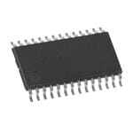
| 产品图片 |
|
| rohs | 符合RoHS |
| 产品系列 | 时钟和计时器IC,时钟发生器及支持产品,IDT 841664AGILF |
| 产品型号 | 841664AGILF |
| 产品种类 | 时钟发生器及支持产品 |
| 占空比-最大 | 53 % |
| 商标 | IDT |
| 安装风格 | SMD/SMT |
| 封装 | Tube |
| 封装/箱体 | TSSOP-28 |
| 工作电源电压 | 3.3 V |
| 工作电源电流 | 80 mA |
| 工厂包装数量 | 48 |
| 最大工作温度 | + 85 C |
| 最大输入频率 | 25 MHz |
| 最大输出频率 | 156.25 MHz |
| 最小工作温度 | - 40 C |
| 类型 | Clock Generators |
| 系列 | 841664I |
| 输出端数量 | 5 |
| 输出类型 | HCSL, LVCMOS |
| 零件号别名 | 841664I ICS841664AGILF |


- 商务部:美国ITC正式对集成电路等产品启动337调查
- 曝三星4nm工艺存在良率问题 高通将骁龙8 Gen1或转产台积电
- 太阳诱电将投资9.5亿元在常州建新厂生产MLCC 预计2023年完工
- 英特尔发布欧洲新工厂建设计划 深化IDM 2.0 战略
- 台积电先进制程称霸业界 有大客户加持明年业绩稳了
- 达到5530亿美元!SIA预计今年全球半导体销售额将创下新高
- 英特尔拟将自动驾驶子公司Mobileye上市 估值或超500亿美元
- 三星加码芯片和SET,合并消费电子和移动部门,撤换高东真等 CEO
- 三星电子宣布重大人事变动 还合并消费电子和移动部门
- 海关总署:前11个月进口集成电路产品价值2.52万亿元 增长14.8%


PDF Datasheet 数据手册内容提取
FemtoClock Crystal-to-HCSL ICS841664I ® Clock Generator DATA SHEET General Description Features The ICS841664I is an optimized sRIO clock generator and a • Four differential HCSL clock outputs: configurable for sRIO member of the family of high-performance clock solutions from IDT. (125MHz or 156.25MHz) clock signals The device uses a 25MHz parallel crystal to generate 125MHz and One REF_OUT LVCMOS/LVTTL clock output 156.25MHz clock signals, replacing solution requiring multiple oscillator and fanout buffer solutions. The device has excellent phase • Selectable crystal oscillator interface, 25MHz, 18pF parallel jitter (<1ps RMS) suitable to clock components requiring precise and resonant crystal or LVCMOS/LVTTL single-ended reference clock low-jitter sRIO clock signals. Designed for telecom, networking and input or LVCMOS/LVTTL single-ended input industrial application, the ICS841664I can also drive the high-speed sRIO SerDes clock inputs of communication processors, DSPs, • Supports the following output frequencies: 125MHz or 156.25MHz switches and bridges. • VCO: 625MHz • Supports PLL bypass and output enable functions • RMS phase jitter, using a 25MHz crystal (1.875MHz - 20MHz): 0.45ps (typical) @ 125MHz • Full 3.3V power supply mode • -40°C to 85°C ambient operating temperature • Lead-free (RoHS 6) packaging Block Diagram Pin Assignment VDD 1 28 IREF XTAL_IN REF_OUT 2 27 FSEL0 1 QA0 25MHz OSC 0 GND 3 26 FSEL1 XTAL_OUT FemtoClock nQA0 QA0 4 25 QB0 fref PLL 0 ÷NA nQA0 5 24 nQB0 REF_IN Pulldown 1 VCO = 625MHz QA1 VDDOA 6 23 VDDOB GND 7 22 GND nQA1 REF_SEL Pulldown QA1 8 21 QB1 nQA1 9 20 nQB1 M =÷25 nREF_OE 10 19 MR/nOE QB0 IREF BYPASS 11 18 VDD nQB0 REF_IN 12 17 XTAL_IN ÷NB REF_SEL 13 16 XTAL_OUT BYPASS Pulldown QB1 VDDA 14 15 GND FSEL[0:1] Pulldown nQB1 ICS841664I MR/nOE Pulldown 28-Lead TSSOP 6.1mm x 9.7mm x 0.925mm REF_OUT package body G Package nREF_OE Pullup Top View ICS841664AGI REVISION A JULY 15, 2013 1 ©2013 Integrated Device Technology, Inc.
ICS841664I Data Sheet FEMTOCLOCK® CRYSTAL-TO-HCSL CLOCK GENERATOR Pin Description and Pin Characteristic Tables Table 1. Pin Descriptions Number Name Type Description 1, 18 V Power Core supply pins. DD 2 REF_OUT Output LVCMOS/LVTTL reference frequency clock output. 3, 7, 15, 22 GND Power Power supply ground. 4, 5, QA0, nQA0 Output Differential Bank A output pairs. HCSL interface levels. 8, 9 QA1, nQA1 6 V Power Output supply pin for Bank A outputs. DDOA Active low REF_OUT enable/disable. See Table 3E. 10 nREF_OE Input Pullup LVCMOS/LVTTL interface levels. 11 BYPASS Input Pulldown Selects PLL/PLL bypass mode. See Table 3C. LVCMOS/LVTTL interface levels. 12 REF_IN Input Pulldown LVCMOS/LVTTL reference clock input. Reference select, Selects the input reference source. See Table 3B. 13 REF_SEL Input Pulldown LVCMOS/LVTTL interface levels 14 V Power Analog supply pin. DDA 16, XTAL_OUT, Parallel resonant crystal interface. XTAL_OUT is the output, Input 17 XTAL_IN XTAL_IN is the input. Active HIGH master reset. Active LOW output enable. When logic HIGH, the internal dividers are reset and the outputs are in high impedance. When logic 19 MR/nOE Input Pulldown LOW, the internal dividers and the outputs are enabled. See Table 3D. LVCMOS/LVTTL interface levels. 20, 21, nQB1, QB1 Output Differential Bank B output pairs. HCSL interface levels. 24, 25 nQB0, QB0 23 V Power Output supply pin for Bank B outputs. DDOB 26, FSEL1, Input Pulldown Output frequency select pins. LVCMOS/LVTTL interface levels. 27 FSEL0 HCSL current reference resistor output. A fixed precision resistor (475) form this 28 IREF Output pin to ground provides a reference current used for differential current-mode QX[0:1], nQX[0:1] clock outputs. NOTE: Pullup and Pulldown refer to internal input resistors. See Table 2, Pin Characteristics, for typical values. Table 2. Pin Characteristics Symbol Parameter Test Conditions Minimum Typical Maximum Units C Input Capacitance 4 pF IN C Power Dissipation Capacitance V = 3.465V 4 pF PD DD R Input Pullup Resistor 51 k PULLUP R Input Pulldown Resistor 51 k PULLDOWN R Output Impedance REF_OUT V = 3.465V 20 OUT DD ICS841664AGI REVISION A JULY 15, 2013 2 ©2013 Integrated Device Technology, Inc.
ICS841664I Data Sheet FEMTOCLOCK® CRYSTAL-TO-HCSL CLOCK GENERATOR Function Tables Table 3A. NA, NB FSELx Function Table (f = 25MHz) ref Inputs Outputs Frequency Settings FSEL1 FSEL0 M QA[0:1], nQA[0:1] QB[0:1], nQB[0:1] 0 0 25 VCO/5 (125MHz) VCO/5 (125MHz) 0 1 25 VCO/5 (125MHz) VCO/4 (156.25MHz) 1 0 25 VCO/5 (125MHz) QB0:1 = L, nQB0:1 = H 1 1 25 VCO/4 (156.25MHz) VCO/4 (156.25MHz) Table 3B. REF_SEL Function Table Input REF_SEL Input Reference 0 XTAL 1 REF_IN Table 3C. BYPASS Function Table Input BYPASS PLL Configuration NOTE 1 0 PLL enabled 1 PLL bypassed (QA, QB = fref/Nx, x = A or B) NOTE 1: Asynchronous control. Table 3D. MR/nOE Function Table Input MR/nOE Function NOTE 1 0 Outputs enabled 1 Internal dividers reset, outputs disabled (High impedance) NOTE 1: Asynchronous control. Table 3E. nREF_OE Function Table Input nREF_OE Function NOTE 1 0 REF_OUT enabled 1 REF_OUT disabled (high impedance) NOTE 1: Asynchronous control. ICS841664AGI REVISION A JULY 15, 2013 3 ©2013 Integrated Device Technology, Inc.
ICS841664I Data Sheet FEMTOCLOCK® CRYSTAL-TO-HCSL CLOCK GENERATOR Absolute Maximum Ratings NOTE: Stresses beyond those listed under Absolute Maximum Ratings may cause permanent damage to the device. These ratings are stress specifications only. Functional operation of product at these conditions or any conditions beyond those listed in the DC Characteristics or AC Characteristics is not implied. Exposure to absolute maximum rating conditions for extended periods may affect product reliability. Item Rating Supply Voltage, V 4.6V DD Inputs, V I XTAL_IN 0V to V DD Other Inputs -0.5V to V + 0.5V DD Outputs,I O Continuous Current REF_OUT 15mA Surge Current REF_OUT 30mA Package Thermal Impedance, 64.5C/W (0 mps) JA Storage Temperature, T -65C to 150C STG DC Electrical Characteristics Table 4A. Power Supply DC Characteristics, V = V = V = 3.3V±5%, T = -40°C to 85°C DD DDOA DDOB A Symbol Parameter Test Conditions Minimum Typical Maximum Units V Core Supply Voltage 3.135 3.3 3.465 V DD V Analog Supply Voltage V – 0.20 3.3 3.465 V DDA DD V DDOA, Output Supply Voltage 3.135 3.3 3.465 V V DDOB I Power Supply Current No Load 80 mA DD I Analog Supply Current No Load 20 mA DDA I DDOA, Output Supply Current No Load, R = 475% 5 mA I REF DDOB Table 4B. LVCMOS/LVTTL DC Characteristics, V = 3.3V±5%, T = -40°C to 85°C DD A Symbol Parameter Test Conditions Minimum Typical Maximum Units V Input High Voltage 2 V + 0.3 V IH DD V Input Low Voltage -0.3 0.8 V IL REF_IN, REF_SEL, BYPASS, MR/nOE, V = V = 3.465V 150 µA DD IN IIH Input High Current FSEL0, FSEL1 nREF_OE V = V = 3.465V 5 µA DD IN REF_IN, REF_SEL, BYPASS, MR/nOE, V = 3.465V, V = 0V -5 µA DD IN IIL Input Low Current FSEL0, FSEL1 nREF_OE V = 3.465V, V = 0V -150 µA DD IN Output High Voltage; V REF_OUT V = 3.465V 2.6 V OH NOTE 1 DD Output Low Voltage; V REF_OUT V = 3.465V 0.5 V OL NOTE 1 DD NOTE 1: Outputs termination with 50 to V /2. See Parameter Measurement Information Section, Output Load Test Circuit diagram. DD ICS841664AGI REVISION A JULY 15, 2013 4 ©2013 Integrated Device Technology, Inc.
ICS841664I Data Sheet FEMTOCLOCK® CRYSTAL-TO-HCSL CLOCK GENERATOR Table 5. Crystal Characteristics Parameter Test Conditions Minimum Typical Maximum Units Mode of Oscillation Fundamental Frequency 25 MHz Equivalent Series Resistance (ESR) 50 Shunt Capacitance 7 pF NOTE: Characterized using an 18pF parallel resonant crystal. AC Electrical Characteristics Table 6A. LVCMOS AC Characteristics, V = 3.3V±5%, T = -40°C to 85°C DD A Symbol Parameter Test Conditions Minimum Typical Maximum Units f Output Frequency REF_OUT 25 MHz OUT t / t Output Rise/Fall Time 20% to 80% 1.5 2.2 ns R F odc Output Duty Cycle 47 53 % ICS841664AGI REVISION A JULY 15, 2013 5 ©2013 Integrated Device Technology, Inc.
ICS841664I Data Sheet FEMTOCLOCK® CRYSTAL-TO-HCSL CLOCK GENERATOR Table 6B. HCSL AC Characteristics, V = V = V = 3.3V±5%, T = -40°C to 85°C DD DDOA DDOB A Symbol Parameter Test Conditions Minimum Typical Maximum Units VCO/5 125 MHz f Output Frequency OUT VCO/4 156.25 MHz 125MHz, Integration Range: 0.45 0.55 ps 1.875MHz - 20MHz tjit(Ø) RMS Phase Jitter (Random); NOTE 1 156.25MHz, Integration Range: 0.41 0.54 ps 1.875MHz - 20MHz tjit(cc) Cycle-to-Cycle Jitter; NOTE 3 60 ps Output Skew; QAx, nQAx, tsk(o) 140 ps NOTE 2, 3 QBx, nQBx t PLL Lock Time 100 ms L V Voltage High 650 700 950 mV HIGH V Voltage Low -150 150 mV LOW V Max. Voltage, Overshoot 0.3 V OVS V Min. Voltage, Undershoot -0.3 V UDS V Ringback Voltage 0.2 V RB V Absolute Crossing Voltage 200 550 mV CROSS Total Variation of V V CROSS 160 mV CROSS over all edges QAx, nQAx, measured between t / t Output Rise/Fall Time 100 700 ps R F QBx, nQBx 0.175V to 0.525V t / t Rise/Fall Time Variation 125 ps R F QAx, nQAx, odc Output Duty Cycle 47 53 % QBx, nQBx NOTE: Electrical parameters are guaranteed over the specified ambient operating temperature range, which is established when the device is mounted in a test socket with maintained transverse airflow greater than 500 lfpm. The device will meet specifications after thermal equilibrium has been reached under these conditions. NOTE: All measurements are taken at 125MHz and 156.25MHz. NOTE 1: Please refer to the Phase Noise Plot. NOTE 2: Defined as skew between outputs at the same supply voltage and with equal load conditions. Measured at the differential cross points. NOTE 3: This parameter is defined in accordance with JEDEC Standard 65. ICS841664AGI REVISION A JULY 15, 2013 6 ©2013 Integrated Device Technology, Inc.
ICS841664I Data Sheet FEMTOCLOCK® CRYSTAL-TO-HCSL CLOCK GENERATOR Typical Phase Noise at 125MHz At 3.3V 125MHz RMS Phase Jitter (Random) 1.875MHz to 20MHz = 0.45ps typical) c BHz d r e w o P e s oi N Offset Frequency (Hz) Typical Phase Noise at 156.25MHz At 3.3V 156.25MHz RMS Phase Jitter (Random) 1.875MHz to 20MHz = 0.41ps typical c BHz d r e w o P e s oi N Offset Frequency (Hz) ICS841664AGI REVISION A JULY 15, 2013 7 ©2013 Integrated Device Technology, Inc.
ICS841664I Data Sheet FEMTOCLOCK® CRYSTAL-TO-HCSL CLOCK GENERATOR Parameter Measurement Information 3.3V±5% 3.3V±5% 3.3V±5% 3.3V±5% Measurement VVVDDDDDD,OOABVDDA VVVDDDDDD,OOABVDDA Qx Point 2pF MenaQsxurement Point IREF GND 2pF 0V 0V 3.3V HCSL Output Load Test Circuit 3.3V HCSL Output Load Test Circuit 1.65V±5% 1.65V±5% SCOPE V DD V DD, V VDDA Qx VDDOAVDDA DDOB GND -1.65V±5% 3.3V LVCMOS Output Load Test Circuit RMS Phase Jitter nQA[0:1], nQx nQB[0:1] QA[0:1], Qx QB[0:1] nQy tcycle n tcycle n+1 tjit(cc) = |tcycle n – tcycle n+1| Qy 1000 Cycles Cycle-to-Cycle Jitter HCSL Output Skew ICS841664AGI REVISION A JULY 15, 2013 8 ©2013 Integrated Device Technology, Inc.
ICS841664I Data Sheet FEMTOCLOCK® CRYSTAL-TO-HCSL CLOCK GENERATOR Parameter Measurement Information, continued V DD 80% 80% 2 REF_OUT t Qx PW 20% 20% t REF_OUT PERIOD t t R F t nQx odc = PW x 100% t PERIOD LVCMOS Output Rise/Fall Time LVCMOS Output Duty Cycle/Pulse Width/Period nQAx, nQBx 0.525V 0.525V V SWING 0.175V 0.175V QAx, QBx t t R F Differential Measurement Points For Rise/Fall Time Differential Measurement Points For Duty Cycle/Period _Delta= 140mV SE Measurement Points For Delta Cross Point Differential Measurement Points For Ringback ICS841664AGI REVISION A JULY 15, 2013 9 ©2013 Integrated Device Technology, Inc.
ICS841664I Data Sheet FEMTOCLOCK® CRYSTAL-TO-HCSL CLOCK GENERATOR Parameter Measurement Information, continued = -0.30V SE Measurement Points For Absolute Cross Point/Swing Applications Information Recommendations for Unused Input and Output Pins Inputs: Outputs: Crystal Inputs HCSL Outputs For applications not requiring the use of the crystal oscillator input, All unused HCSL outputs can be left floating. We recommend that both XTAL_IN and XTAL_OUT can be left floating. Though not there is no trace attached. Both sides of the differential output pair required, but for additional protection, a 1k resistor can be tied from should either be left floating or terminated. XTAL_IN to ground. LVCMOS Outputs REF_CLK Input The unused LVCMOS output can be left floating. There should be no For applications not requiring the use of the reference clock, it can be trace attached. left floating. Though not required, but for additional protection, a 1k resistor can be tied from the REF_CLK to ground. LVCMOS Control Pins All control pins have internal pullups and pulldowns; additional resistance is not required but can be added for additional protection. A 1k resistor can be used. ICS841664AGI REVISION A JULY 15, 2013 10 ©2013 Integrated Device Technology, Inc.
ICS841664I Data Sheet FEMTOCLOCK® CRYSTAL-TO-HCSL CLOCK GENERATOR Schematic Layout Figure 1 shows an example of ICS841664I application schematic. In adjusting C1 and C2. For this device, the crystal load capacitors are this example, the device is operated at V = V = V = required for proper operation. DD DDA DDOA V = 3.3V. The 18pF parallel resonant 25MHz crystal is used. DDOB As with any high speed analog circuitry, the power supply pins are The load capacitance C1 = 27pF and C2 = 27pF are recommended vulnerable to random noise. To achieve optimum jitter performance, for frequency accuracy. Depending on the parasitic of the printed power supply isolation is required. The ICS841664I provides circuit board layout, these values might require a slight adjustment to separate power supplies to isolate any high switching noise from optimize the frequency accuracy. Crystals with other load coupling into the internal PLL. capacitance specifications can be used. This will require R1 33 Zo = 50 REF_OUT Logic Control Input Examples LVCMOS Set Logic Set Logic VDD VDD Input to Input to '1' '0' R2 R3 33 475 QB0 Zo = 50 RU1 RU2 + 1K Not Install VDD U1 R4 33 To Logic To Logic nQB0 Zo = 50 - Input Input 1 28 pins pins 2 VDD IREF 27 FSEL0 RD1 RD2 3 REF_OUT FSEL0 26 FSEL1 VDDO R5 R6 Not Install 1K VDDO 4 GND FSEL1 25 50 50 Recommended for PCI 5 QA0 QB0 24 6 nQA0 nQB0 23 Express Add-In Card 78 VGDNDDOA VDDGNOBD 2212 QB1 9 QA1 QB1 20 nQB1 nREF_OE 10 nQA1 nQB1 19 MR/nOE VDD BYPASS 11 nREF_OE MR/nOE 18 VDD=3.3V REF_IN 12 BYPASS VDD 17 VDD REF_SEL 13 REF_IN XTAL_IN 16 VDDOA=3.3V Q1 14 REF_SEL XTAL_OUT 15 HCSL Termination VDDA GND VDDOB=3.3V Ro ~ 7 Ohm R12 Zo = 50 Ohm 43 Optional Driver_LVCMOS R8 0-33 Zo = 50 + R7 VDD 10 VDDA R9 0-33 X1 Zo = 50 C3 C1 25MHz - C4 27pF 18pF 10u 0.1u HCSL Optional Termination R10 R11 Recommended for PCI C2 50 50 27pF Express Point-to-Point Connection 3.3V 3.3V BLM18BB221SN1 BLM18BB221SN2 (U1:1) (U1:18) 1 2 VDD 1 2 (U1:6) (U1:23)VDDO Ferrite Bead C6 C7 C8 Ferrite Bead C10 C11 C12 C5 C9 0.1uF 10uF 0.1uF 0.1uF 0.1uF 10uF 0.1uF 0.1uF Figure 1. ICS841664I Schematic Example In order to achieve the best possible filtering, it is recommended that is known, such as switching power supplies frequencies, it is the placement of the filter components be on the device side of the recommended that component values be adjusted and if required, PCB as close to the power pins as possible. If space is limited, the additional filtering be added. Additionally general design practice for 0.1µF capacitor in each power pin filter should be placed on the power plane voltage stability suggests adding bulk capacitances in device side of the PCB and the other components can be placed on the general area of all devices. the opposite side. The schematic example focuses on functional connections and is not Power supply filter recommendations are a general guideline to be configuration specific. Refer to the pin description and functional used for reducing external noise from coupling into the devices. The tables in the datasheet to ensure the logic control inputs are properly filter performance is designed for wide range of noise frequency. This set. low-pass filter starts to attenuate noise at approximately 10kHz. If a specific frequency noise component with high amplitude interference ICS841664AGI REVISION A JULY 15, 2013 11 ©2013 Integrated Device Technology, Inc.
ICS841664I Data Sheet FEMTOCLOCK® CRYSTAL-TO-HCSL CLOCK GENERATOR Overdriving the XTAL Interface The XTAL_IN input can be overdriven by an LVCMOS driver or by one can be done in one of two ways. First, R1 and R2 in parallel should side of a differential driver through an AC coupling capacitor. The equal the transmission line impedance. For most 50 applications, XTAL_OUT pin can be left floating. The amplitude of the input signal R1 and R2 can be 100. This can also be accomplished by removing should be between 500mV and 1.8V and the slew rate should not be R1 and changing R2 to 50. The values of the resistors can be less than 0.2V/nS. For 3.3V LVCMOS inputs, the amplitude must be increased to reduce the loading for a slower and weaker LVCMOS reduced from full swing to at least half the swing in order to prevent driver. Figure 2B shows an example of the interface diagram for an signal interference with the power rail and to reduce internal noise. LVPECL driver. This is a standard LVPECL termination with one side Figure 2A shows an example of the interface diagram for a high of the driver feeding the XTAL_IN input. It is recommended that all speed 3.3V LVCMOS driver. This configuration requires that the sum components in the schematics be placed in the layout. Though some of the output impedance of the driver (Ro) and the series resistance components might not be used, they can be utilized for debugging (Rs) equals the transmission line impedance. In addition, matched purposes. The datasheet specifications are characterized and termination at the crystal input will attenuate the signal in half. This guaranteed by using a quartz crystal as the input. VCC XTAL_OUT R1 100 Ro Rs Zo = 50 ohms C1 XTAL_IN R2 .1uf Zo = Ro + Rs 100 LVCMOS Driver Figure 2A. General Diagram for LVCMOS Driver to XTAL Input Interface XTAL_OUT C2 Zo = 50 ohms XTAL_IN Zo = 50 ohms .1uf LVPECL Driver R1 R2 50 50 R3 50 Figure 2B. General Diagram for LVPECL Driver to XTAL Input Interface ICS841664AGI REVISION A JULY 15, 2013 12 ©2013 Integrated Device Technology, Inc.
ICS841664I Data Sheet FEMTOCLOCK® CRYSTAL-TO-HCSL CLOCK GENERATOR Applications Information, continued Recommended Termination Figure 3A is the recommended source termination for applications All traces should be 50Ω impedance single-ended or where the driver and receiver will be on a separate PCBs. This 100Ω differential. termination is the standard for PCI Express™ and HCSL output types. Rs 0.5" Max 0-0.2" 1-14" 0.5 - 3.5" 22 to 33 +/-5% L1 L2 L4 L5 L1 L2 L4 L5 PCI Express PCI Express Connector Driver PCI Express 0-0.2" L3 L3 Add-in Card Rt 49.9 +/- 5% Figure 3A. Recommended Source Termination (where the driver and receiver will be on separate PCBs) Figure 3B is the recommended termination for applications where a be minimized. In addition, a series resistor (Rs) at the driver point-to-point connection can be used. A point-to-point connection offers flexibility and can help dampen unwanted reflections. contains both the driver and the receiver on the same PCB. With a The optional resistor can range from 0Ω to 33Ω. All traces matched termination at the receiver, transmission-line reflections will should be 50Ω impedance single-ended or 100Ω differential. Rs 0.5" Max 0-18" 0-0.2" 0 to 33 L1 L2 L3 0 to 33 L1 L2 L3 PCI Express Driver Rt 49.9 +/- 5% Figure 3B. Recommended Termination (where a point-to-point connection can be used) ICS841664AGI REVISION A JULY 15, 2013 13 ©2013 Integrated Device Technology, Inc.
ICS841664I Data Sheet FEMTOCLOCK® CRYSTAL-TO-HCSL CLOCK GENERATOR Power Considerations This section provides information on power dissipation and junction temperature for the ICS841664I. Equations and example calculations are also provided. 1. Power Dissipation. The total power dissipation for the ICS841664I is the total power minus the analog power plus the power dissipated into the load. The following is the power dissipation for V = 3.3V + 5% = 3.465V, which gives worst case results. DD Core and HCSL Output Power Dissipation (cid:129) Power (core) = V * (I + I ) = 3.465V * (80mA + 20mA) = 346.5mW MAX DD_MAX DD_MAX DDA_MAX (cid:129) Power (outputs) = 44.5mW/Loaded Output pair MAX If all outputs are loaded, the total power is 4 * 44.5mW = 178mW LVCMOS Driver Power Dissipation (cid:129) Dynamic Power Dissipation at 25MHz Power (25MHz) = C * Frequency * (V )2 = 4pF * 25MHz * (3.465V)2 = 1.20mW per output PD DD Total Power Dissipation (cid:129) Total Power = Power (core) + Power (Outputs) + Total Power (25MHz) = 346.5mW + 178mW + 1.2mW = 525.7mW 2. Junction Temperature. Junction temperature, Tj, is the temperature at the junction of the bond wire and bond pad directly affects the reliability of the device. The maximum recommended junction temperature is 125°C. Limiting the internal transistor junction temperature, Tj, to 125°C ensures that the bond wire and bond pad temperature remains below 125°C. The equation for Tj is as follows: Tj = * Pd_total + T JA A Tj = Junction Temperature = Junction-to-Ambient Thermal Resistance JA Pd_total = Total Device Power Dissipation (example calculation is in section 1 above) T = Ambient Temperature A In order to calculate junction temperature, the appropriate junction-to-ambient thermal resistance must be used. Assuming no air flow and JA a multi-layer board, the appropriate value is 64.5°C/W per Table 7 below. Therefore, Tj for an ambient temperature of 85°C with all outputs switching is: 85°C + 0.526W * 64.3°C/W = 118.9°C. This is below the limit of 125°C. This calculation is only an example. Tj will obviously vary depending on the number of loaded outputs, supply voltage, air flow and the type of board (multi-layer). Table 7. Thermal Resistance for 28 Lead TSSOP, Forced Convection JA by Velocity JA Meters per Second 0 1 2.5 Multi-Layer PCB, JEDEC Standard Test Boards 64.5°C/W 60.4°C/W 58.5°C/W ICS841664AGI REVISION A JULY 15, 2013 14 ©2013 Integrated Device Technology, Inc.
ICS841664I Data Sheet FEMTOCLOCK® CRYSTAL-TO-HCSL CLOCK GENERATOR 3. Calculations and Equations. The purpose of this section is to calculate power dissipation on the IC per HCSL output pair. HCSL output driver circuit and termination are shown in Figure 4. VDD IOUT = 17mA V OUT RREF = 475 ± 1% R L 50 IC Figure 4. HCSL Driver Circuit and Termination HCSL is a current steering output which sources a maximum of 17mA of current per output. To calculate worst case on-chip power dissipation, use the following equations which assume a 50 load to ground. The highest power dissipation occurs when V _ . DD MAX Power = (V – V ) * I DD_MAX OUT OUT since V = I * R OUT OUT L Power = (V – I * R ) * I DD_MAX OUT L OUT = (3.465V – 17mA * 50) * 17mA Total Power Dissipation per output pair = 44.5mW ICS841664AGI REVISION A JULY 15, 2013 15 ©2013 Integrated Device Technology, Inc.
ICS841664I Data Sheet FEMTOCLOCK® CRYSTAL-TO-HCSL CLOCK GENERATOR Reliability Information Table 8. vs. Air Flow Table for a 28 Lead TSSOP JA by Velocity JA Meters per Second 0 1 2.5 Multi-Layer PCB, JEDEC Standard Test Boards 64.5°C/W 60.4°C/W 58.5°C/W Transistor Count The transistor count for ICS841664I is: 2954 Package Outline and Package Dimensions Package Outline - G Suffix for 28 Lead TSSOP Table 9. Package Dimensions All Dimensions in Millimeters Symbol Minimum Maximum N 28 A 1.20 A1 0.05 0.15 A2 0.80 1.05 b 0.19 0.30 c 0.09 0.20 D 9.60 9.80 E 8.10 Basic E1 6.00 6.20 e 0.65 Basic L 0.45 0.75 0° 8° aaa 0.10 Reference Document: JEDEC Publication 95, MO-153 ICS841664AGI REVISION A JULY 15, 2013 16 ©2013 Integrated Device Technology, Inc.
ICS841664I Data Sheet FEMTOCLOCK® CRYSTAL-TO-HCSL CLOCK GENERATOR Ordering Information Table 10. Ordering Information Part/Order Number Marking Package Shipping Packaging Temperature 841664AGILF ICS841664AGI 28 Lead “Lead-Free” TSSOP Tube -40C to 85C 841664AGILFT ICS841664AGI 28 Lead “Lead-Free” TSSOP Tape & Reel -40C to 85C ICS841664AGI REVISION A JULY 15, 2013 17 ©2013 Integrated Device Technology, Inc.
ICS841664I Data Sheet FEMTOCLOCK® CRYSTAL-TO-HCSL CLOCK GENERATOR Revision History Sheet Rev Table Page Description of Change Date T1 2 Pin Description Table - switched pin names for pins 20 through 25. A 7/15/13 T10 18 Ordering Information Table - deleted Tape & Reel quantity. ICS841664AGI REVISION A JULY 15, 2013 18 ©2013 Integrated Device Technology, Inc.
ICS841664I Data Sheet FEMTOCLOCK® CRYSTAL-TO-HCSL CLOCK GENERATOR We’ve Got Your Timing Solution 6024 Silver Creek Valley Road Sales Technical Support Sales San Jose, California 95138 800-345-7015 (inside USA) netcom@idt.com +408-284-8200 (outside USA) +480-763-2056 Fax: 408-284-2775 www.IDT.com/go/contactIDT DISCLAIMER Integrated Device Technology, Inc. (IDT) and its subsidiaries reserve the right to modify the products and/or specifications described herein at any time and at IDT’s sole discretion. All information in this document, including descriptions of product features and performance, is subject to change without notice. Performance specifications and the operating parameters of the described products are determined in the independent state and are not guaranteed to perform the same way when installed in customer products. The information contained herein is provided without representation or warranty of any kind, whether express or implied, including, but not limited to, the suitability of IDT’s products for any particular purpose, an implied warranty of merchantability, or non-infringement of the intellectual property rights of others. This document is presented only as a guide and does not convey any license under intellectual property rights of IDT or any third parties. IDT’s products are not intended for use in applications involving extreme environmental conditions or in life support systems or similar devices where the failure or malfunction of an IDT product can be reasonably expected to signifi- cantly affect the health or safety of users. Anyone using an IDT product in such a manner does so at their own risk, absent an express, written agreement by IDT. Integrated Device Technology, IDT and the IDT logo are registered trademarks of IDT. Other trademarks and service marks used herein, including protected names, logos and designs, are the property of IDT or their respective third party owners. Copyright 2013. All rights reserved.
Mouser Electronics Authorized Distributor Click to View Pricing, Inventory, Delivery & Lifecycle Information: I DT (Integrated Device Technology): 841664AGILF 841664AGILFT