ICGOO在线商城 > 集成电路(IC) > 逻辑 - 缓冲器,驱动器,接收器,收发器 > 74VHCT125PW,118
 Datasheet下载
- 型号: 74VHCT125PW,118
- 制造商: NXP Semiconductors
- 库位|库存: xxxx|xxxx
- 要求:
| 数量阶梯 | 香港交货 | 国内含税 |
| +xxxx | $xxxx | ¥xxxx |
查看当月历史价格
查看今年历史价格
74VHCT125PW,118产品简介:
ICGOO电子元器件商城为您提供74VHCT125PW,118由NXP Semiconductors设计生产,在icgoo商城现货销售,并且可以通过原厂、代理商等渠道进行代购。 74VHCT125PW,118价格参考。NXP Semiconductors74VHCT125PW,118封装/规格:逻辑 - 缓冲器,驱动器,接收器,收发器, Buffer, Non-Inverting 4 Element 1 Bit per Element 3-State Output 14-TSSOP。您可以下载74VHCT125PW,118参考资料、Datasheet数据手册功能说明书,资料中有74VHCT125PW,118 详细功能的应用电路图电压和使用方法及教程。
Nexperia USA Inc. 生产的74VHCT125PW,118是一款逻辑缓冲器,属于74系列高速CMOS器件。它具有低功耗、高噪声容限和兼容TTL电平的特点,广泛应用于各种数字电路设计中。

 应用场景

1. 信号缓冲与驱动:
   - 该芯片主要用于信号的缓冲和驱动,能够增强信号的驱动能力,确保信号在长距离传输或复杂电路中不失真。例如,在PCB板上连接多个负载时,可以使用74VHCT125来保证信号的完整性和稳定性。

2. 电平转换:
   - 74VHCT125支持3.3V和5V逻辑电平之间的转换,适用于混合电压系统中的电平匹配。例如,在一个包含3.3V微控制器和5V外设的系统中,该芯片可以作为电平转换器,确保两者之间正确通信。

3. 多路选择与分配:
   - 由于其四通道的设计,74VHCT125可以用于多路信号的选择和分配。例如,在需要将一个输入信号分发到多个输出端口的应用中,它可以起到关键作用。

4. 总线隔离:
   - 在复杂的总线系统中,74VHCT125可以用作总线隔离器,防止不同模块之间的干扰。特别是在多处理器或分布式控制系统中,它可以有效隔离各个模块,提高系统的稳定性和可靠性。

5. 接口扩展:
   - 当需要扩展I/O接口时,74VHCT125可以作为一个简单的扩展方案。例如,在嵌入式系统中,当主控芯片的I/O引脚不足时,可以通过74VHCT125增加额外的控制引脚。

6. 时钟信号处理:
   - 在时钟分配网络中,74VHCT125可以用来缓冲时钟信号,减少时钟抖动和延迟,确保时钟信号的同步性和准确性。

总之,74VHCT125PW,118凭借其高性能和多功能性,广泛应用于各种数字电路中,特别是在需要信号增强、电平转换、多路选择和总线隔离等场合,是工程师们常用的逻辑器件之一。
| 参数 | 数值 |
| 产品目录 | 集成电路 (IC)半导体 |
| 描述 | IC BUFFER/LINE DVR QUAD 14TSSOP缓冲器和线路驱动器 CMOS 4CH NON-INVERT |
| 产品分类 | |
| 品牌 | NXP Semiconductors |
| 产品手册 | |
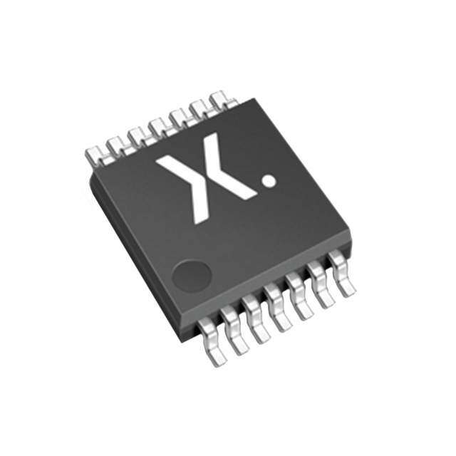
| 产品图片 |
|
| rohs | 符合RoHS无铅 / 符合限制有害物质指令(RoHS)规范要求 |
| 产品系列 | 逻辑集成电路,缓冲器和线路驱动器,NXP Semiconductors 74VHCT125PW,11874VHCT |
| 数据手册 | |
| 产品型号 | 74VHCT125PW,118 |
| PCN封装 | |
| PCN组件/产地 | |
| 产品培训模块 | http://www.digikey.cn/PTM/IndividualPTM.page?site=cn&lang=zhs&ptm=25224 |
| 产品种类 | 缓冲器和线路驱动器 |
| 传播延迟时间 | 7.5 ns at 4.5 V to 5.5 V |
| 低电平输出电流 | 8 mA |
| 供应商器件封装 | 14-TSSOP |
| 元件数 | 4 |
| 其它名称 | 568-5178-1 |
| 包装 | 剪切带 (CT) |
| 商标 | NXP Semiconductors |
| 安装类型 | 表面贴装 |
| 安装风格 | SMD/SMT |
| 封装 | Reel |
| 封装/外壳 | 14-TSSOP(0.173",4.40mm 宽) |
| 封装/箱体 | TSSOP-14 |
| 工作温度 | -40°C ~ 125°C |
| 工厂包装数量 | 2500 |
| 最大工作温度 | + 125 C |
| 最小工作温度 | - 40 C |
| 极性 | Non-Inverting |
| 标准包装 | 1 |
| 每元件位数 | 1 |
| 每芯片的通道数量 | 4 |
| 电压-电源 | 4.5 V ~ 5.5 V |
| 电流-输出高,低 | 8mA,8mA |
| 电源电压-最大 | 5.5 V |
| 电源电压-最小 | 4.5 V |
| 输入线路数量 | 4 |
| 输出类型 | 3-State |
| 输出线路数量 | 4 |
| 逻辑类型 | CMOS |
| 逻辑系列 | VHCT |
| 高电平输出电流 | - 8 mA |


- 商务部:美国ITC正式对集成电路等产品启动337调查
- 曝三星4nm工艺存在良率问题 高通将骁龙8 Gen1或转产台积电
- 太阳诱电将投资9.5亿元在常州建新厂生产MLCC 预计2023年完工
- 英特尔发布欧洲新工厂建设计划 深化IDM 2.0 战略
- 台积电先进制程称霸业界 有大客户加持明年业绩稳了
- 达到5530亿美元!SIA预计今年全球半导体销售额将创下新高
- 英特尔拟将自动驾驶子公司Mobileye上市 估值或超500亿美元
- 三星加码芯片和SET,合并消费电子和移动部门,撤换高东真等 CEO
- 三星电子宣布重大人事变动 还合并消费电子和移动部门
- 海关总署:前11个月进口集成电路产品价值2.52万亿元 增长14.8%


PDF Datasheet 数据手册内容提取
74VHC125; 74VHCT125 Quad buffer/line driver; 3-state Rev. 02 — 13 October 2009 Product data sheet 1. General description The 74VHC125; 74VHCT125 are high-speed Si-gate CMOS devices and are pin compatiblewithLow-powerSchottkyTTL(LSTTL).Theyarespecifiedincompliancewith JEDEC standard JESD7-A. The 74VHC125; 74VHCT125 provides four non-inverting buffer/line drivers with 3-state outputs.The3-stateoutputs(nY)arecontrolledbytheoutputenableinput(nOE).AHIGH at nOE causes the outputs to assume a high-impedance OFF-state. The74VHC125;74VHCT125areidenticaltothe74VHC126;74VHCT126buthaveactive LOW enable inputs. 2. Features n Balanced propagation delays n All inputs have a Schmitt-trigger action n Inputs accepts voltages higher thanV CC n Input levels: u The 74VHC125 operates with CMOS logic levels u The 74VHCT125 operates with TTL logic levels n ESD protection: u HBM JESD22-A114E exceeds 2000V u MM JESD22-A115-A exceeds 200V u CDM JESD22-C101C exceeds 1000V n Multiple package options n Specified from-40 (cid:176)C to +85 (cid:176)C and from -40 (cid:176)C to +125 (cid:176)C 3. Ordering information Table 1. Ordering information Type number Package Temperature range Name Description Version 74VHC125D -40 (cid:176)Cto+125 (cid:176)C SO14 plastic small outline package; 14leads; SOT108-1 bodywidth3.9mm 74VHCT125D 74VHC125PW -40 (cid:176)Cto+125 (cid:176)C TSSOP14 plastic thin shrink small outline package; 14leads; SOT402-1 body width 4.4mm 74VHCT125PW 74VHC125BQ -40 (cid:176)Cto+125 (cid:176)C DHVQFN14 plastic dual in-line compatible thermal enhanced very SOT762-1 thin quad flat package; no leads; 14 terminals; 74VHCT125BQ body2.5· 3· 0.85mm
74VHC125; 74VHCT125 Nexperia Quad buffer/line driver; 3-state 4. Functional diagram 2 1A 1Y 3 2 1 1 1OE 3 1 5 2A 2Y 6 EN1 5 4 2OE 6 4 9 3A 3Y 8 9 8 10 3OE 10 12 4A 4Y 11 nA nY 12 11 13 4OE 13 nOE mna228 mna229 mna227 Fig 1. Logic symbol Fig 2. IEC logic symbol Fig 3. Logic diagram (one buffer) 5. Pinning information 5.1 Pinning 74VHC125 74VHCT125 E C terminal 1 O C 74VHC125 index area 1 V 74VHCT125 1 14 1A 2 13 4OE 1OE 1 14 VCC 1Y 3 12 4A 1A 2 13 4OE 2OE 4 11 4Y 1Y 3 12 4A 2A 5 GND(1) 10 3OE 2OE 4 11 4Y 2Y 6 9 3A 2A 5 10 3OE 7 8 2Y 6 9 3A D Y GND 7 8 3Y GN 3 001aak045 001aak044 Transparent top view (1) The die substrate is attached to this pad using conductive die attach material. It can not be used as a supply pin or input. Fig 4. Pin configuration SO14 and TSSOP14 Fig 5. Pin configuration DHVQFN14 74VHC_VHCT125_2 © Nexperia B.V. 2017. All rights reserved Product data sheet Rev. 02 — 13 October 2009 2 of 15
74VHC125; 74VHCT125 Nexperia Quad buffer/line driver; 3-state 5.2 Pin description Table 2. Pin description Symbol Pin Description 1OE, 2OE, 3OE, 4OE 1, 4, 10, 13 output enable input (active LOW) 1A, 2A, 3A, 4A 2, 5, 9, 12 data input 1Y, 2Y, 3Y, 4Y 3, 6, 8, 11 data output GND 7 ground (0V) V 14 supply voltage CC 6. Functional description Table 3. Function table[1] Control Input Output nOE nA nY L L L H H H X Z [1] H=HIGH voltage level; L=LOW voltage level; X=don’t care; Z=high-impedance OFF-state. 7. Limiting values Table 4. Limiting values In accordance with the Absolute Maximum Rating System (IEC 60134).Voltages are referenced to GND (ground = 0V). Symbol Parameter Conditions Min Max Unit V supply voltage -0.5 +7.0 V CC V input voltage -0.5 +7.0 V I I input clamping current V <-0.5V [1] -20 - mA IK I I output clamping current V <-0.5V orV >V +0.5V [1] - –20 mA OK O O CC I output current V =-0.5V to (V +0.5V) - –25 mA O O CC I supply current - 75 mA CC I ground current -75 - mA GND T storage temperature -65 +150 (cid:176)C stg P total power dissipation T =-40 (cid:176)C to +125 (cid:176)C tot amb SO14 package [2] - 500 mW TSSOP14 package [3] - 500 mW DHVQFN14 package [4] - 500 mW [1] The input and output voltage ratings may be exceeded if the input and output current ratings are observed. [2] P derates linearly with 8mW/K above 70(cid:176)C. tot [3] P derates linearly with 5.5mW/K above 60(cid:176)C. tot [4] P derates linearly with 4.5mW/K above 60(cid:176)C. tot 74VHC_VHCT125_2 © Nexperia B.V. 2017. All rights reserved Product data sheet Rev. 02 — 13 October 2009 3 of 15
74VHC125; 74VHCT125 Nexperia Quad buffer/line driver; 3-state 8. Recommended operating conditions Table 5. Recommended operating conditions Voltages are referenced to GND (ground = 0 V). Symbol Parameter Conditions 74VHC125 74VHCT125 Unit Min Typ Max Min Typ Max V supply voltage 2.0 5.0 5.5 4.5 5.0 5.5 V CC V input voltage 0 - 5.5 0 - 5.5 V I V output voltage 0 - V 0 - V V O CC CC T ambient temperature -40 +25 +125 -40 +25 +125 (cid:176)C amb Dt/DV input transition rise V = 3.3 V– 0.3 V - - 100 - - - ns/V CC and fall rate V = 5.0 V– 0.5 V - - 20 - - 20 ns/V CC 9. Static characteristics Table 6. Static characteristics Voltages are referenced to GND (ground = 0 V). Symbol Parameter Conditions 25(cid:176)C -40 (cid:176)C to+85 (cid:176)C - 40(cid:176)C to+125 (cid:176)C Unit Min Typ Max Min Max Min Max For type 74VHC125 V HIGH-level V = 2.0 V 1.5 - - 1.5 - 1.5 - V IH CC input voltage V = 3.0 V 2.1 - - 2.1 - 2.1 - V CC V = 5.5 V 3.85 - - 3.85 - 3.85 - V CC V LOW-level V = 2.0 V - - 0.5 - 0.5 - 0.5 V IL CC input voltage V = 3.0 V - - 0.9 - 0.9 - 0.9 V CC V = 5.5 V - - 1.65 - 1.65 - 1.65 V CC V HIGH-level V = V or V OH I IH IL output voltage I =-50 mA; V =2.0 V 1.9 2.0 - 1.9 - 1.9 - V O CC I =-50 mA; V =3.0 V 2.9 3.0 - 2.9 - 2.9 - V O CC I =-50 mA; V =4.5 V 4.4 4.5 - 4.4 - 4.4 - V O CC I =-4.0mA; V =3.0 V 2.58 - - 2.48 - 2.40 - V O CC I =-8.0mA; V =4.5 V 3.94 - - 3.8 - 3.70 - V O CC V LOW-level V = V or V OL I IH IL output voltage I = 50mA; V =2.0 V - 0 0.1 - 0.1 - 0.1 V O CC I = 50mA; V =3.0 V - 0 0.1 - 0.1 - 0.1 V O CC I = 50mA; V =4.5 V - 0 0.1 - 0.1 - 0.1 V O CC I = 4.0mA; V =3.0 V - - 0.36 - 0.44 - 0.55 V O CC I = 8.0mA; V =4.5 V - - 0.36 - 0.44 - 0.55 V O CC I OFF-state V =V orV ; - - –0.25 - –2.5 - –10.0 mA OZ I IH IL output current V =V orGND; O CC V =5.5V CC I input leakage V =5.5 VorGND; - - 0.1 - 1.0 - 2.0 mA I I current V =0Vto5.5V CC I supply current V =V orGND; I = 0 A; - - 2.0 - 20 - 40 mA CC I CC O V =5.5V CC 74VHC_VHCT125_2 © Nexperia B.V. 2017. All rights reserved Product data sheet Rev. 02 — 13 October 2009 4 of 15
74VHC125; 74VHCT125 Nexperia Quad buffer/line driver; 3-state Table 6. Static characteristics …continued Voltages are referenced to GND (ground = 0 V). Symbol Parameter Conditions 25(cid:176)C -40 (cid:176)C to+85 (cid:176)C - 40(cid:176)C to+125 (cid:176)C Unit Min Typ Max Min Max Min Max C input - 3.0 10 - 10 - 10 pF I capacitance C output - 4.0 - - - - - pF O capacitance For type 74VHCT125 V HIGH-level V = 4.5 V to 5.5 V 2.0 - - 2.0 - 2.0 - V IH CC input voltage V LOW-level V = 4.5 V to 5.5 V - - 0.8 - 0.8 - 0.8 V IL CC input voltage V HIGH-level V = V or V ; V =4.5 V OH I IH IL CC output voltage I =-50 mA 4.4 4.5 - 4.4 - 4.4 - V O I =-8.0mA 3.94 - - 3.8 - 3.70 - V O V LOW-level V = V or V ; V =4.5 V OL I IH IL CC output voltage I = 50mA - 0 0.1 - 0.1 - 0.1 V O I = 8.0mA - - 0.36 - 0.44 - 0.55 V O I OFF-state per input pin; V =V orV ; - - –0.25 - –2.5 - –10.0 mA OZ I IH IL output current V =5.5V; I =0 A CC O V =V orGND; O CC otherpinsatV or GND CC I input leakage V =5.5 VorGND; - - 0.1 - 1.0 - 2.0 mA I I current V =0Vto5.5V CC I supply current V =V orGND; I = 0 A; - - 2.0 - 20 - 40 mA CC I CC O V =5.5V CC DI additional per input pin; - - 1.35 - 1.5 - 1.5 mA CC supply current V =V - 2.1V; I =0 A; I CC O otherpinsatV or GND; CC V =4.5Vto5.5V CC C input - 3.0 10 - 10 - 10 pF I capacitance C output - 4.0 - - - - - pF O capacitance 74VHC_VHCT125_2 © Nexperia B.V. 2017. All rights reserved Product data sheet Rev. 02 — 13 October 2009 5 of 15
74VHC125; 74VHCT125 Nexperia Quad buffer/line driver; 3-state 10. Dynamic characteristics Table 7. Dynamic characteristics GND = 0 V; For test circuit seeFigure8. Symbol Parameter Conditions 25(cid:176)C -40 (cid:176)C to+85 (cid:176)C -40 (cid:176)C to+125 (cid:176)C Unit Min Typ[1] Max Min Max Min Max For type 74VHC125 t propagation nAtonY; seeFigure6 [2] pd delay V = 3.0 V to 3.6 V CC C =15pF - 4.4 8.0 1.0 9.5 1.0 11.5 ns L C =50pF - 6.2 11.5 1.0 13.0 1.0 14.5 ns L V = 4.5 V to 5.5 V CC C =15pF - 3.0 5.5 1.0 6.5 1.0 7.0 ns L C =50pF - 4.3 7.5 1.0 8.5 1.0 9.5 ns L t enable time nOEtonY; seeFigure7 [2] en V = 3.0 V to 3.6 V CC C =15pF - 4.7 8.0 1.0 9.5 1.0 11.5 ns L C =50pF - 6.8 11.5 1.0 13.0 1.0 14.5 ns L V = 4.5 V to 5.5 V CC C =15pF - 3.3 5.1 1.0 6.0 1.0 6.5 ns L C =50pF - 4.7 7.1 1.0 8.0 1.0 9.0 ns L t disable time nOEtonY; seeFigure7 [2] dis V = 3.0 V to 3.6 V CC C =15pF - 6.7 9.7 1.0 11.5 1.0 12.5 ns L C =50pF - 9.6 13.2 1.0 15.0 1.0 16.5 ns L V = 4.5 V to 5.5 V CC C =15pF - 4.8 6.8 1.0 8.0 1.0 8.5 ns L C =50pF - 6.8 8.8 1.0 10.0 1.0 11.0 ns L C power C =50pF; f = 1 MHz; [3] - 10 - - - - - pF PD L i dissipation V =GNDtoV I CC capacitance 74VHC_VHCT125_2 © Nexperia B.V. 2017. All rights reserved Product data sheet Rev. 02 — 13 October 2009 6 of 15
74VHC125; 74VHCT125 Nexperia Quad buffer/line driver; 3-state Table 7. Dynamic characteristics …continued GND = 0 V; For test circuit seeFigure8. Symbol Parameter Conditions 25(cid:176)C -40 (cid:176)C to+85 (cid:176)C -40 (cid:176)C to+125 (cid:176)C Unit Min Typ[1] Max Min Max Min Max For type 74VHCT125 t propagation nAtonY; seeFigure6 [2] pd delay V = 4.5 V to 5.5 V CC C =15pF - 3.0 5.5 1.0 6.5 1.0 7.0 ns L C =50pF - 4.3 7.5 1.0 8.5 1.0 9.5 ns L t enable time nOEtonY; seeFigure7 en V = 4.5 V to 5.5 V CC C =15pF - 3.4 5.1 1.0 6.0 1.0 6.5 ns L C =50pF - 4.9 7.3 1.0 8.3 1.0 9.5 ns L t disable time nOEtonY; seeFigure7 [2] dis V = 4.5 V to 5.5 V CC C =15pF - 4.5 6.8 1.0 8.0 1.0 8.5 ns L C =50pF - 6.5 8.8 1.0 10.0 1.0 11.0 ns L C power C =50pF; f = 1 MHz; [3] - 12 - - - - - pF PD L i dissipation V =GNDtoV I CC capacitance [1] Typical values are measured at nominal supply voltage (V = 3.3V and V = 5.0V). CC CC [2] t is the same as t and t . pd PLH PHL t is the same as t and t . en PZL PZH t is the same as t and t . dis PLZ PHZ [3] C is used to determine the dynamic power dissipation (P inm W). PD D P =C · V 2· f · N+S(C · V 2· f )where: D PD CC i L CC o f = input frequency in MHz, f =output frequency in MHz i o C =output load capacitance inpF L V =supply voltage in Volts CC N= number of inputs switching S (C · V 2· f )=sum of the outputs. L CC o 11. Waveforms VI nA input VM GND tPHL tPLH VOH nY output VM VOL mna230 Measurement points are given inTable8. V and V are typical voltage output levels that occur with the output load. OL OH Fig 6. Propagation delay input (nA) to output (nY) 74VHC_VHCT125_2 © Nexperia B.V. 2017. All rights reserved Product data sheet Rev. 02 — 13 October 2009 7 of 15
74VHC125; 74VHCT125 Nexperia Quad buffer/line driver; 3-state VI nOE input VM GND tPLZ tPZL VCC output LOW-to-OFF VM OFF-to-LOW VOL VX tPHZ tPZH VOH VY output HIGH-to-OFF VM OFF-to-HIGH GND outputs outputs outputs enabled disabled enabled mna362 Measurement points are given inTable8. V and V are typical voltage output levels that occur with the output load. OL OH Fig 7. Enable and disable times Table 8. Measurement points Type Input Output V V V V M M X Y 74VHC125 0.5V 0.5V V + 0.3 V V - 0.3 V CC CC OL OL 74VHCT125 1.5V 0.5V V + 0.3 V V - 0.3 V CC OL OL 74VHC_VHCT125_2 © Nexperia B.V. 2017. All rights reserved Product data sheet Rev. 02 — 13 October 2009 8 of 15
74VHC125; 74VHCT125 Nexperia Quad buffer/line driver; 3-state tW VI 90 % negative pulse VM VM 10 % 0 V tf tr tr tf VI 90 % positive pulse VM VM 10 % 0 V tW VCC VCC VI VO RL S1 G DUT open RT CL 001aad983 Test data is given inTable9. Definitions test circuit: R = Termination resistance should be equal to output impedance Z of the pulse generator. T o C = Load capacitance including jig and probe capacitance. L R = Load resistance. L S1 = Test selection switch. Fig 8. Load circuit for switching times Table 9. Test data Type Input Load S1 position V t, t C R t , t t , t t , t I r f L L PHL PLH PZH PHZ PZL PLZ 74VHC125 V £ 3.0 ns 15 pF, 50 pF 1kW open GND V CC CC 74VHCT125 3.0 V £ 3.0 ns 15 pF, 50 pF 1kW open GND V CC 74VHC_VHCT125_2 © Nexperia B.V. 2017. All rights reserved Product data sheet Rev. 02 — 13 October 2009 9 of 15
74VHC125; 74VHCT125 Nexperia Quad buffer/line driver; 3-state 12. Package outline SO14: plastic small outline package; 14 leads; body width 3.9 mm SOT108-1 D E A X c y HE v M A Z 14 8 Q A2 A1 (A 3 ) A pin 1 index q Lp 1 7 L e w M detail X bp 0 2.5 5 mm scale DIMENSIONS (inch dimensions are derived from the original mm dimensions) UNIT mAax. A1 A2 A3 bp c D(1) E(1) e HE L Lp Q v w y Z(1) q 0.25 1.45 0.49 0.25 8.75 4.0 6.2 1.0 0.7 0.7 mm 1.75 0.25 1.27 1.05 0.25 0.25 0.1 0.10 1.25 0.36 0.19 8.55 3.8 5.8 0.4 0.6 0.3 8o 0.010 0.057 0.019 0.0100 0.35 0.16 0.244 0.039 0.028 0.028 0o inches 0.069 0.01 0.05 0.041 0.01 0.01 0.004 0.004 0.049 0.014 0.0075 0.34 0.15 0.228 0.016 0.024 0.012 Note 1. Plastic or metal protrusions of 0.15 mm (0.006 inch) maximum per side are not included. OUTLINE REFERENCES EUROPEAN ISSUE DATE VERSION IEC JEDEC JEITA PROJECTION 99-12-27 SOT108-1 076E06 MS-012 03-02-19 Fig 9. Package outline SOT108-1 (SO14) 74VHC_VHCT125_2 © Nexperia B.V. 2017. All rights reserved Product data sheet Rev. 02 — 13 October 2009 10 of 15
74VHC125; 74VHCT125 Nexperia Quad buffer/line driver; 3-state TSSOP14: plastic thin shrink small outline package; 14 leads; body width 4.4 mm SOT402-1 D E A X c y HE v M A Z 14 8 Q A2 (A 3 ) A pin 1 index A1 q Lp L 1 7 detail X w M e bp 0 2.5 5 mm scale DIMENSIONS (mm are the original dimensions) UNIT mAax. A1 A2 A3 bp c D(1) E(2) e HE L Lp Q v w y Z(1) q mm 1.1 00..1055 00..9850 0.25 00..3109 00..21 54..19 44..53 0.65 66..62 1 00..7550 00..43 0.2 0.13 0.1 00..7328 80oo Notes 1. Plastic or metal protrusions of 0.15 mm maximum per side are not included. 2. Plastic interlead protrusions of 0.25 mm maximum per side are not included. OUTLINE REFERENCES EUROPEAN ISSUE DATE VERSION IEC JEDEC JEITA PROJECTION 99-12-27 SOT402-1 MO-153 03-02-18 Fig 10. Package outline SOT402-1 (TSSOP14) 74VHC_VHCT125_2 © Nexperia B.V. 2017. All rights reserved Product data sheet Rev. 02 — 13 October 2009 11 of 15
74VHC125; 74VHCT125 Nexperia Quad buffer/line driver; 3-state DHVQFN14: plastic dual in-line compatible thermal enhanced very thin quad flat package; no leads; 14 terminals; body 2.5 x 3 x 0.85 mm SOT762-1 D B A A A1 E c terminal 1 detail X index area terminal 1 e1 C index area e b v M C A B y1 C y w M C 2 6 L 1 7 Eh e 14 8 13 9 Dh X 0 2.5 5 mm scale DIMENSIONS (mm are the original dimensions) A(1) UNIT max. A1 b c D(1) Dh E(1) Eh e e1 L v w y y1 0.05 0.30 3.1 1.65 2.6 1.15 0.5 mm 1 0.2 0.5 2 0.1 0.05 0.05 0.1 0.00 0.18 2.9 1.35 2.4 0.85 0.3 Note 1. Plastic or metal protrusions of 0.075 mm maximum per side are not included. OUTLINE REFERENCES EUROPEAN ISSUE DATE VERSION IEC JEDEC JEITA PROJECTION 02-10-17 SOT762-1 - - - MO-241 - - - 03-01-27 Fig 11. Package outline SOT762-1 (DHVQFN14) 74VHC_VHCT125_2 © Nexperia B.V. 2017. All rights reserved Product data sheet Rev. 02 — 13 October 2009 12 of 15
74VHC125; 74VHCT125 Nexperia Quad buffer/line driver; 3-state 13. Abbreviations Table 10. Abbreviations Acronym Description CMOS Complementary Metal Oxide Semiconductor LSTTL Low-power Schottky Transistor-Transistor Logic ESD ElectroStatic Discharge HBM Human Body Model MM Machine Model CDM Charge-Device Model TTL Transistor-Transistor Logic 14. Revision history Table 11. Revision history Document ID Release date Data sheet status Change notice Supersedes 74VHC_VHCT125_2 20091013 Product data sheet - 74VHC_VHCT125_1 Modifications: • Errata in features list corrected. 74VHC_VHCT125_1 20090630 Product data sheet - - 74VHC_VHCT125_2 © Nexperia B.V. 2017. All rights reserved Product data sheet Rev. 02 — 13 October 2009 13 of 15
74VHC125; 74VHCT125 Nexperia Quad buffer/line driver; 3-state 15. Legal information 15.1 Data sheet status Document status[1][2] Product status[3] Definition Objective [short] data sheet Development This document contains data from the objective specification for product development. Preliminary [short] data sheet Qualification This document contains data from the preliminary specification. Product [short] data sheet Production This document contains the product specification. [1] Please consult the most recently issued document before initiating or completing a design. [2] The term ‘short data sheet’ is explained in section “Definitions”. [3] Theproductstatusofdevice(s)describedinthisdocumentmayhavechangedsincethisdocumentwaspublishedandmaydifferincaseofmultipledevices.Thelatestproductstatus information is available on the Internet at URLhttp://www.nexperia.com. 15.2 Definitions damage. Nexperia accepts no liability for inclusion and/or use of Nexperia products in such equipment or applications and therefore such inclusion and/or use is at the customer’s own risk. Draft —The document is a draft version only. The content is still under internal review and subject to formal approval, which may result in Applications —Applications that are described herein for any of these modifications or additions. Nexperia does not give any products are for illustrative purposes only. Nexperia makes no representations or warranties as to the accuracy or completeness of representation or warranty that such applications will be suitable for the informationincludedhereinandshallhavenoliabilityfortheconsequencesof specified use without further testing or modification. use of such information. Limiting values —Stress above one or more limiting values (as defined in Short data sheet —A short data sheet is an extract from a full data sheet theAbsoluteMaximumRatingsSystemofIEC60134)maycausepermanent withthesameproducttypenumber(s)andtitle.Ashortdatasheetisintended damagetothedevice.Limitingvaluesarestressratingsonlyandoperationof forquickreferenceonlyandshouldnotbereliedupontocontaindetailedand the device at these or any other conditions above those given in the full information. For detailed and full information see the relevant full data Characteristics sections of this document is not implied. Exposure to limiting sheet, which is available on request via the local Nexperia sales values for extended periods may affect device reliability. office. In case of any inconsistency or conflict with the short data sheet, the Terms and conditions of sale —Nexperia products are sold full data sheet shall prevail. subjecttothegeneraltermsandconditionsofcommercialsale,aspublished athttp://www.nexperia.com/profile/terms, including those pertaining to warranty, 15.3 Disclaimers intellectual property rights infringement and limitation of liability, unless explicitly otherwise agreed to in writing by Nexperia. In case of any inconsistency or conflict between information in this document and such General —Information in this document is believed to be accurate and terms and conditions, the latter will prevail. reliable.However,Nexperiadoesnotgiveanyrepresentationsor No offer to sell or license —Nothing in this document may be interpreted warranties,expressedorimplied,astotheaccuracyorcompletenessofsuch or construed as an offer to sell products that is open for acceptance or the information and shall have no liability for the consequences of use of such grant,conveyanceorimplicationofanylicenseunderanycopyrights,patents information. or other industrial or intellectual property rights. Right to make changes —Nexperiareservestherighttomake Export control —This document as well as the item(s) described herein changes to information published in this document, including without may be subject to export control regulations. Export might require a prior limitation specifications and product descriptions, at any time and without authorization from national authorities. notice.Thisdocumentsupersedesandreplacesallinformationsuppliedprior to the publication hereof. Suitability for use —Nexperia products are not designed, 15.4 Trademarks authorized or warranted to be suitable for use in medical, military, aircraft, space or life support equipment, nor in applications where failure or Notice:Allreferencedbrands,productnames,servicenamesandtrademarks malfunction of a Nexperia product can reasonably be expected are the property of their respective owners. to result in personal injury, death or severe property or environmental 16. Contact information For more information, please visit:http://www.nexperia.com For sales office addresses, please send an email to:salesaddresses@nexperia.com 74VHC_VHCT125_2 © Nexperia B.V. 2017. All rights reserved Product data sheet Rev. 02 — 13 October 2009 14 of 15
74VHC125; 74VHCT125 Nexperia Quad buffer/line driver; 3-state 17. Contents 1 General description. . . . . . . . . . . . . . . . . . . . . . 1 2 Features . . . . . . . . . . . . . . . . . . . . . . . . . . . . . . . 1 3 Ordering information. . . . . . . . . . . . . . . . . . . . . 1 4 Functional diagram . . . . . . . . . . . . . . . . . . . . . . 2 5 Pinning information. . . . . . . . . . . . . . . . . . . . . . 2 5.1 Pinning . . . . . . . . . . . . . . . . . . . . . . . . . . . . . . . 2 5.2 Pin description . . . . . . . . . . . . . . . . . . . . . . . . . 3 6 Functional description . . . . . . . . . . . . . . . . . . . 3 7 Limiting values. . . . . . . . . . . . . . . . . . . . . . . . . . 3 8 Recommended operating conditions. . . . . . . . 4 9 Static characteristics. . . . . . . . . . . . . . . . . . . . . 4 10 Dynamic characteristics . . . . . . . . . . . . . . . . . . 6 11 Waveforms . . . . . . . . . . . . . . . . . . . . . . . . . . . . . 7 12 Package outline . . . . . . . . . . . . . . . . . . . . . . . . 10 13 Abbreviations. . . . . . . . . . . . . . . . . . . . . . . . . . 13 14 Revision history. . . . . . . . . . . . . . . . . . . . . . . . 13 15 Legal information. . . . . . . . . . . . . . . . . . . . . . . 14 15.1 Data sheet status . . . . . . . . . . . . . . . . . . . . . . 14 15.2 Definitions. . . . . . . . . . . . . . . . . . . . . . . . . . . . 14 15.3 Disclaimers. . . . . . . . . . . . . . . . . . . . . . . . . . . 14 15.4 Trademarks. . . . . . . . . . . . . . . . . . . . . . . . . . . 14 16 Contact information. . . . . . . . . . . . . . . . . . . . . 14 17 Contents. . . . . . . . . . . . . . . . . . . . . . . . . . . . . . 15 © Nexperia B.V. 2017. All rights reserved For more information, please visit: http://www.nexperia.com For sales office addresses, please send an email to: salesaddresses@nexperia.com Date of release: 13 October 2009