ICGOO在线商城 > 集成电路(IC) > 逻辑 - 栅极和逆变器 > 74VHC08SJX
 Datasheet下载
- 型号: 74VHC08SJX
- 制造商: Fairchild Semiconductor
- 库位|库存: xxxx|xxxx
- 要求:
| 数量阶梯 | 香港交货 | 国内含税 |
| +xxxx | $xxxx | ¥xxxx |
查看当月历史价格
查看今年历史价格
74VHC08SJX产品简介:
ICGOO电子元器件商城为您提供74VHC08SJX由Fairchild Semiconductor设计生产,在icgoo商城现货销售,并且可以通过原厂、代理商等渠道进行代购。 74VHC08SJX价格参考。Fairchild Semiconductor74VHC08SJX封装/规格:逻辑 - 栅极和逆变器, AND Gate IC 4 Channel 14-SOP。您可以下载74VHC08SJX参考资料、Datasheet数据手册功能说明书,资料中有74VHC08SJX 详细功能的应用电路图电压和使用方法及教程。
ON Semiconductor的74VHC08SJX是一款四路双输入与门(AND Gate)逻辑集成电路,属于74VHC系列。它具有低功耗、高噪声容限和宽电源电压范围等特点,适用于多种数字电路设计。以下是其主要应用场景:

1. 数字信号处理:
   - 74VHC08SJX常用于需要对多个输入信号进行逻辑“与”操作的场合。例如,在数据传输系统中,它可以用来检测多个条件是否同时满足,从而触发特定的操作或事件。

2. 时序控制:
   - 在时钟同步和定时电路中,该芯片可以用于生成精确的时序信号。通过组合多个与门,可以实现复杂的时序逻辑,确保各个模块在正确的时间点协同工作。

3. 传感器融合:
   - 当多个传感器输出需要综合判断时,74VHC08SJX可以帮助整合这些信息。例如,在安全系统中,只有当多个传感器(如红外探测器和压力传感器)同时触发时,才发出警报信号。

4. 接口电路:
   - 在不同设备之间的通信接口中,74VHC08SJX可用于信号调理和协议转换。它可以确保只有在所有必要的握手信号都有效的情况下,才会允许数据传输。

5. 嵌入式系统:
   - 在微控制器或单片机外围电路中,该芯片可以用作辅助逻辑单元,简化主处理器的负担。例如,在智能家电或工业控制系统中,它可以帮助实现更高效的资源管理和任务调度。

6. 消费电子:
   - 在电视、音响等消费电子产品中,74VHC08SJX可以用于音频视频切换、电源管理等功能,提高产品的可靠性和性能。

总之,74VHC08SJX凭借其稳定的性能和广泛的适用性,在各种数字电路设计中发挥着重要作用,尤其适合需要高效、可靠的逻辑运算和信号处理的应用场景。
| 参数 | 数值 |
| 产品目录 | 集成电路 (IC)半导体 |
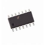
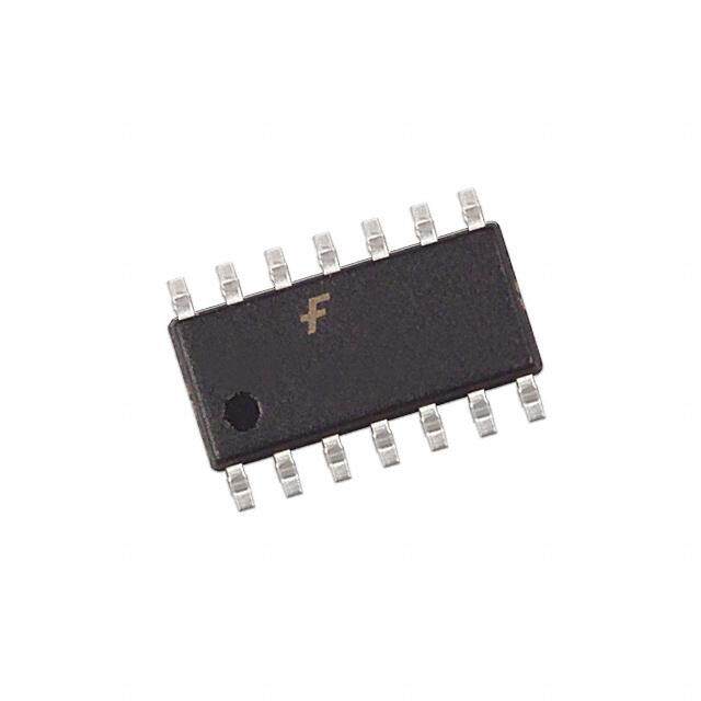
| 描述 | IC GATE AND 4CH 2-INP 14-SOIC逻辑门 Qd 2-Input AND Gate |
| 产品分类 | |
| 品牌 | Fairchild Semiconductor |
| 产品手册 | |
| 产品图片 |
|
| rohs | 符合RoHS无铅 / 符合限制有害物质指令(RoHS)规范要求 |
| 产品系列 | 逻辑集成电路,逻辑门,Fairchild Semiconductor 74VHC08SJX74VHC |
| 数据手册 | |
| 产品型号 | 74VHC08SJX |
| 不同V、最大CL时的最大传播延迟 | 7.9ns @ 5V,50pF |
| 产品 | AND |
| 产品种类 | 逻辑门 |
| 传播延迟时间 | 12.3 ns |
| 低电平输出电流 | 8 mA |
| 供应商器件封装 | 14-SOIC |
| 其它名称 | 74VHC08SJXDKR |
| 包装 | Digi-Reel® |
| 单位重量 | 218.300 mg |
| 商标 | Fairchild Semiconductor |
| 安装类型 | 表面贴装 |
| 安装风格 | SMD/SMT |
| 封装 | Reel |
| 封装/外壳 | 14-SOIC(0.209",5.30mm 宽) |
| 封装/箱体 | SOP-14 |
| 工作温度 | -40°C ~ 85°C |
| 工厂包装数量 | 2000 |
| 最大工作温度 | + 85 C |
| 最小工作温度 | - 40 C |
| 栅极数量 | 4 Gate |
| 标准包装 | 1 |
| 特性 | - |
| 电压-电源 | 2 V ~ 5.5 V |
| 电流-输出高,低 | 8mA,8mA |
| 电流-静态(最大值) | 2µA |
| 电源电压-最大 | 5.5 V |
| 电源电压-最小 | 2 V |
| 电路数 | 4 |
| 系列 | 74VHC08 |
| 输入/输出线数量 | 2 / 1 |
| 输入数 | 2 |
| 输入线路数量 | 2 |
| 输出线路数量 | 1 |
| 逻辑电平-低 | 0.5V |
| 逻辑电平-高 | 1.5V |
| 逻辑类型 | 与门 |
| 逻辑系列 | 74VHC |
| 高电平输出电流 | - 8 mA |


PDF Datasheet 数据手册内容提取
Is Now Part of To learn more about ON Semiconductor, please visit our website at www.onsemi.com Please note: As part of the Fairchild Semiconductor integration, some of the Fairchild orderable part numbers will need to change in order to meet ON Semiconductor’s system requirements. Since the ON Semiconductor product management systems do not have the ability to manage part nomenclature that utilizes an underscore (_), the underscore (_) in the Fairchild part numbers will be changed to a dash (-). This document may contain device numbers with an underscore (_). Please check the ON Semiconductor website to verify the updated device numbers. The most current and up-to-date ordering information can be found at www.onsemi.com. Please email any questions regarding the system integration to Fairchild_questions@onsemi.com. ON Semiconductor and the ON Semiconductor logo are trademarks of Semiconductor Components Industries, LLC dba ON Semiconductor or its subsidiaries in the United States and/or other countries. ON Semiconductor owns the rights to a number of patents, trademarks, copyrights, trade secrets, and other intellectual property. A listing of ON Semiconductor’s product/patent coverage may be accessed at www.onsemi.com/site/pdf/Patent-Marking.pdf. ON Semiconductor reserves the right to make changes without further notice to any products herein. ON Semiconductor makes no warranty, representation or guarantee regarding the suitability of its products for any particular purpose, nor does ON Semiconductor assume any liability arising out of the application or use of any product or circuit, and specifically disclaims any and all liability, including without limitation special, consequential or incidental damages. Buyer is responsible for its products and applications using ON Semiconductor products, including compliance with all laws, regulations and safety requirements or standards, regardless of any support or applications information provided by ON Semiconductor. “Typical” parameters which may be provided in ON Semiconductor data sheets and/or specifications can and do vary in different applications and actual performance may vary over time. All operating parameters, including “Typicals” must be validated for each customer application by customer’s technical experts. ON Semiconductor does not convey any license under its patent rights nor the rights of others. ON Semiconductor products are not designed, intended, or authorized for use as a critical component in life support systems or any FDA Class 3 medical devices or medical devices with a same or similar classification in a foreign jurisdiction or any devices intended for implantation in the human body. Should Buyer purchase or use ON Semiconductor products for any such unintended or unauthorized application, Buyer shall indemnify and hold ON Semiconductor and its officers, employees, subsidiaries, affiliates, and distributors harmless against all claims, costs, damages, and expenses, and reasonable attorney fees arising out of, directly or indirectly, any claim of personal injury or death associated with such unintended or unauthorized use, even if such claim alleges that ON Semiconductor was negligent regarding the design or manufacture of the part. ON Semiconductor is an Equal Opportunity/Affirmative Action Employer. This literature is subject to all applicable copyright laws and is not for resale in any manner.
7 4 V H December 2007 C 0 8 — 74VHC08 Q u a Quad 2-Input AND Gate d 2 - I n Features General Description p u ■ High Speed: tPD = 4.3ns (Typ.) at TA = 25°C The VHC08 is an advanced high speed CMOS 2 Input t A ■ High noise immunity: V = V = 28% V (Min.) AND Gate fabricated with silicon gate CMOS technol- N NIH NIL CC ogy. It achieves the high-speed operation similar to D ■ Power down protection is provided on all inputs equivalent Bipolar Schottky TTL while maintaining the G ■ Low power dissipation: I = 2µA (Max.) @ T = 25°C CC A CMOS low power dissipation. a ■ Low noise: VOLP = 0.8V (Max.) te The internal circuit is composed of 4 stages including ■ Pin and function compatible with 74HC08 buffer output, which provide high noise immunity and stable output. An input protection circuit insures that 0V to 7V can be applied to the input pins without regard to the supply voltage. This device can be used to interface 5V to 3V systems and two supply systems such as bat- tery backup. This circuit prevents device destruction due to mismatched supply and input voltages. Ordering Information Package Order Number Number Package Description 74VHC08M M14A 14-Lead Small Outline Integrated Circuit (SOIC), JEDEC MS-012, 0.150" Narrow 74VHC08SJ M14D 14-Lead Small Outline Package (SOP), EIAJ TYPE II, 5.3mm Wide 74VHC08MTC MTC14 14-Lead Thin Shrink Small Outline Package (TSSOP), JEDEC MO-153, 4.4mm Wide Device also available in Tape and Reel. Specify by appending suffix letter “X” to the ordering number. All packages are lead free per JEDEC: J-STD-020B standard. ©1992 Fairchild Semiconductor Corporation www.fairchildsemi.com 74VHC08 Rev. 1.4.0
7 4 Connection Diagram Logic Symbol V H C IEEE/IEC 0 8 — Q u a d 2 - I n p u t A N D G Pin Description a t Truth Table e Pin Names Description A , B Inputs A B O n n O Outputs L L L n L H L H L L H H H ©1992 Fairchild Semiconductor Corporation www.fairchildsemi.com 74VHC08 Rev. 1.4.0 2
7 4 Absolute Maximum Ratings V H Stresses exceeding the absolute maximum ratings may damage the device. The device may not function or be C operable above the recommended operating conditions and stressing the parts to these levels is not recommended. 0 8 In addition, extended exposure to stresses above the recommended operating conditions may affect device reliability. — The absolute maximum ratings are stress ratings only. Q Symbol Parameter Rating u a V Supply Voltage –0.5V to +7.0V d CC 2 V DC Input Voltage –0.5V to +7.0V - IN I n V DC Output Voltage –0.5V to V + 0.5V p OUT CC u IIK Input Diode Current –20mA t A I Output Diode Current ±20mA N OK D IOUT DC Output Current ±25mA G I DC V /GND Current ±50mA a CC CC t e T Storage Temperature –65°C to +150°C STG T Lead Temperature (Soldering, 10 seconds) 260°C L Recommended Operating Conditions(1) The Recommended Operating Conditions table defines the conditions for actual device operation. Recommended operating conditions are specified to ensure optimal performance to the datasheet specifications. Fairchild does not recommend exceeding them or designing to absolute maximum ratings. Symbol Parameter Rating V Supply Voltage 2.0V to +5.5V CC V Input Voltage 0V to +5.5V IN V Output Voltage 0V to V OUT CC T Operating Temperature –40°C to +85°C OPR t , t Input Rise and Fall Time, r f V = 3.3V ± 0.3V 0ns/V ∼ 100ns/V CC V = 5.0V ± 0.5V 0ns/V ∼ 20ns/V CC Note: 1. Unused inputs must be held HIGH or LOW. They may not float. ©1992 Fairchild Semiconductor Corporation www.fairchildsemi.com 74VHC08 Rev. 1.4.0 3
7 4 DC Electrical Characteristics V H C TA = –40°C to 0 T = 25°C +85°C 8 A — Symbol Parameter V (V) Conditions Min. Typ. Max. Min. Max. Units CC Q V HIGH Level Input 2.0 1.50 1.50 V IH u Voltage a 3.0–5.5 0.7 x V 0.7 x V CC CC d V LOW Level Input 2.0 0.50 0.50 V 2 IL - Voltage I 3.0–5.5 0.3 x V 0.3 x V n CC CC p VOH HIGH Level 2.0 VIN = VIH IOH = –50µA 1.9 2.0 1.9 V u Output Voltage 3.0 or VIL 2.9 3.0 2.9 t A N 4.5 4.4 4.5 4.4 D 3.0 IOH = –4mA 2.58 2.48 G 4.5 I = –8mA 3.94 3.80 a OH t e V LOW Level 2.0 V = V I = 50µA 0.0 0.1 0.1 V OL IN IH OL Output Voltage or V 3.0 IL 0.0 0.1 0.1 4.5 0.0 0.1 0.1 3.0 I = 4mA 0.36 0.44 OL 4.5 I = 8mA 0.36 0.44 OL I Input Leakage 0–5.5 V = 5.5V or GND ±0.1 ±1.0 µA IN IN Current I Quiescent 5.5 V = V or GND 2.0 20.0 µA CC IN CC Supply Current Noise Characteristics T = 25°C A Symbol Parameter V (V) Conditions Typ. Limits Units CC V (2) Quiet Output Maximum 5.0 C = 50pF 0.3 0.8 V OLP L Dynamic V OL V (2) Quiet Output Minimum 5.0 C = 50pF –0.3 –0.8 V OLV L Dynamic V OL V (2) Minimum HIGH Level 5.0 C = 50pF 3.5 V IHD L Dynamic Input Voltage V 2) Maximum LOW Level 5.0 C = 50pF 1.5 V ILD L Dynamic Input Voltage Note: 2. Parameter guaranteed by design. ©1992 Fairchild Semiconductor Corporation www.fairchildsemi.com 74VHC08 Rev. 1.4.0 4
7 4 AC Electrical Characteristics V H C TA = –40°C 0 T = 25°C to +85°C 8 A — Symbol Parameter V (V) Conditions Min. Typ. Max. Min. Max. Units CC Q t , t Propagation Delay 3.3 ± 0.3 C = 15pF 6.2 8.8 1.0 10.5 ns u PHL PLH L a C = 50pF 8.7 12.3 1.0 14.0 d L 2 5.0 ± 0.5 CL = 15pF 4.3 5.9 1.0 7.0 ns -I n CL = 50pF 5.8 7.9 1.0 9.0 p u CIN Input Capacitance VCC = Open 4 10 10 pF t A CPD Power Dissipation (3) 18 pF N Capacitance D G Note: a 3. CPD is defined as the value of the internal equivalent capacitance which is calculated from the operating te current consumption without load. Average operating current can be obtained by the equation: I (opr.) = C • V • f + I / 4 (per gate). CC PD CC IN CC ©1992 Fairchild Semiconductor Corporation www.fairchildsemi.com 74VHC08 Rev. 1.4.0 5
0.65 (cid:24)(cid:17)(cid:19)(cid:19)(cid:147)(cid:19)(cid:17)(cid:20)(cid:19) A 0.43TYP 14 8 B 6.4 (cid:23)(cid:17)(cid:23)(cid:19)(cid:147)(cid:19)(cid:17)(cid:20)(cid:19) 6.10 3.2 1.65 1 7 0.2 C B A PIN1IDENT TOPVIEW ALLLEADTIPS 0.45 RECOMMENDEDLANDPATTERN 1.2MAX SEEDETAILA +0.15 0.90 -0.10 0.20 (cid:19)(cid:17)(cid:20)(cid:19)(cid:147)(cid:19)(cid:17)(cid:19)(cid:24) 0.09 ALLLEADTIPS 0.30 0.19 C 0.1 C 0.65 0.13 A B C (cid:20)(cid:21)(cid:17)(cid:19)(cid:19)(cid:131)(cid:3)(cid:55)(cid:50)(cid:51)(cid:3)(cid:9)(cid:3)(cid:37)(cid:50)(cid:55)(cid:55)(cid:50)(cid:48) FRONTVIEW 0.09MIN NOTES: GAGEPLANE A.CONFORMSTOJEDECREGISTRATIONMO-153, VARIATIONAB,REFNOTE6 B.DIMENSIONSAREINMILLIMETERS. 0.25 0.09MIN C.DIMENSIONSAREEXCLUSIVEOFBURRS, (cid:19)(cid:131)(cid:16)(cid:3)(cid:27)(cid:131) (cid:19)(cid:17)(cid:25)(cid:147)(cid:19)(cid:17)(cid:20) MOLDFLASH,ANDTIEBAREXTRUSIONS SEATINGPLANE 1.00 D.DIMENSIONINGANDTOLERANCESPERANSI DETAILA Y14.5M,2009. E.LANDPATTERNSTANDARD:SOP65P640X110-14M. F.DRAWINGFILENAME:MKT-MTC14rev7.
None
8.75 A 8.50 7.62 14 0.65 8 14 8 B 4.00 6.00 5.60 3.80 1.70 1 7 PIN #1 1.27 0.51 1 7 IDENT. 1.27 0.35 (0.33) 0.25 M C B A LAND PATTERN RECOMMENDATION TOP VIEW 1.75 MAX A C 0.25 0.19 1.50 0.10 C 0.25 1.25 0.10 SIDE VIEW FRONT VIEW NOTES: A. CONFORMS TO JEDEC MS-012, VARIATION AB, ISSUE C B. ALL DIMENSIONS ARE IN MILLIMETERS 0.50 0.25 x 45 C. DIMENSIONS DO NOT INCLUDE MOLD FLASH OR BURRS R0.10 GAGE D. LAND PATTERN STANDARD: PLANE SOIC127P600X145-14M R0.10 E. CONFORMS TO ASME Y14.5M, 2009 0.36 D. DRAWING FILENAME: MKT-M14Arev14 8° 0° 0.90 0.50 SEATING PLANE (1.04) DETAIL A SCALE 16 : 1
ON Semiconductor and are trademarks of Semiconductor Components Industries, LLC dba ON Semiconductor or its subsidiaries in the United States and/or other countries. ON Semiconductor owns the rights to a number of patents, trademarks, copyrights, trade secrets, and other intellectual property. A listing of ON Semiconductor’s product/patent coverage may be accessed at www.onsemi.com/site/pdf/Patent−Marking.pdf. ON Semiconductor reserves the right to make changes without further notice to any products herein. ON Semiconductor makes no warranty, representation or guarantee regarding the suitability of its products for any particular purpose, nor does ON Semiconductor assume any liability arising out of the application or use of any product or circuit, and specifically disclaims any and all liability, including without limitation special, consequential or incidental damages. Buyer is responsible for its products and applications using ON Semiconductor products, including compliance with all laws, regulations and safety requirements or standards, regardless of any support or applications information provided by ON Semiconductor. “Typical” parameters which may be provided in ON Semiconductor data sheets and/or specifications can and do vary in different applications and actual performance may vary over time. All operating parameters, including “Typicals” must be validated for each customer application by customer’s technical experts. ON Semiconductor does not convey any license under its patent rights nor the rights of others. ON Semiconductor products are not designed, intended, or authorized for use as a critical component in life support systems or any FDA Class 3 medical devices or medical devices with a same or similar classification in a foreign jurisdiction or any devices intended for implantation in the human body. Should Buyer purchase or use ON Semiconductor products for any such unintended or unauthorized application, Buyer shall indemnify and hold ON Semiconductor and its officers, employees, subsidiaries, affiliates, and distributors harmless against all claims, costs, damages, and expenses, and reasonable attorney fees arising out of, directly or indirectly, any claim of personal injury or death associated with such unintended or unauthorized use, even if such claim alleges that ON Semiconductor was negligent regarding the design or manufacture of the part. ON Semiconductor is an Equal Opportunity/Affirmative Action Employer. This literature is subject to all applicable copyright laws and is not for resale in any manner. PUBLICATION ORDERING INFORMATION LITERATURE FULFILLMENT: N. American Technical Support: 800−282−9855 Toll Free ON Semiconductor Website: www.onsemi.com Literature Distribution Center for ON Semiconductor USA/Canada 19521 E. 32nd Pkwy, Aurora, Colorado 80011 USA Europe, Middle East and Africa Technical Support: Order Literature: http://www.onsemi.com/orderlit Phone: 303−675−2175 or 800−344−3860 Toll Free USA/Canada Phone: 421 33 790 2910 Fax: 303−675−2176 or 800−344−3867 Toll Free USA/Canada Japan Customer Focus Center For additional information, please contact your local Email: orderlit@onsemi.com Phone: 81−3−5817−1050 Sales Representative © Semiconductor Components Industries, LLC www.onsemi.com www.onsemi.com 1
Mouser Electronics Authorized Distributor Click to View Pricing, Inventory, Delivery & Lifecycle Information: O N Semiconductor: 74VHC08MTCX 74VHC08MX 74VHC08SJ 74VHC08SJX 74VHC08M 74VHC08MTC