ICGOO在线商城 > 集成电路(IC) > 逻辑 - 缓冲器,驱动器,接收器,收发器 > 74LVX4245MTCX
 Datasheet下载
- 型号: 74LVX4245MTCX
- 制造商: Fairchild Semiconductor
- 库位|库存: xxxx|xxxx
- 要求:
| 数量阶梯 | 香港交货 | 国内含税 |
| +xxxx | $xxxx | ¥xxxx |
查看当月历史价格
查看今年历史价格
74LVX4245MTCX产品简介:
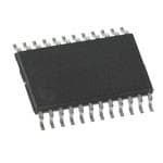
ICGOO电子元器件商城为您提供74LVX4245MTCX由Fairchild Semiconductor设计生产,在icgoo商城现货销售,并且可以通过原厂、代理商等渠道进行代购。 74LVX4245MTCX价格参考¥1.12-¥1.12。Fairchild Semiconductor74LVX4245MTCX封装/规格:逻辑 - 缓冲器,驱动器,接收器,收发器, Transceiver, Non-Inverting 1 Element 8 Bit per Element 3-State Output 24-TSSOP。您可以下载74LVX4245MTCX参考资料、Datasheet数据手册功能说明书,资料中有74LVX4245MTCX 详细功能的应用电路图电压和使用方法及教程。
ON Semiconductor的74LVX4245MTCX是一款低电压CMOS八位双电源电平转换收发器,属于逻辑缓冲器/收发器类别。该器件支持双向数据传输,具备独立的输入/输出电源引脚(VCC(A)和VCC(B)),可在1.65V至3.6V范围内工作,实现1.8V、2.5V、3.3V等不同逻辑电平系统之间的无缝接口。

典型应用场景包括:便携式电子产品(如智能手机、平板电脑)中的I/O电平匹配;嵌入式系统中微控制器与外围设备(如传感器、存储器、FPGA)之间的信号电平转换;通信模块中不同电压域电路的数据交换;以及工业控制板卡中多电压供电系统的信号隔离与驱动。

其TSSOP-24封装具有体积小、引脚间距适中、易于焊接的优点,适合高密度PCB布局。74LVX4245MTCX还具备高抗噪能力、低功耗特性,并支持热插拔操作,适用于对能效和稳定性要求较高的场景。方向控制(DIR)和输出使能(OE)引脚可精确管理数据流向,确保系统通信可靠。
| 参数 | 数值 |
| 产品目录 | 集成电路 (IC)半导体 |
| 描述 | TXRX 8-BIT DUAL 3STATE 24TSSOP总线收发器 8-Bit Dl Supp Trans |
| 产品分类 | |
| 品牌 | Fairchild Semiconductor |
| 产品手册 | |
| 产品图片 |
|
| rohs | 符合RoHS无铅 / 符合限制有害物质指令(RoHS)规范要求 |
| 产品系列 | 逻辑集成电路,总线收发器,Fairchild Semiconductor 74LVX4245MTCX74LVX |
| 数据手册 | |
| 产品型号 | 74LVX4245MTCX |
| 产品培训模块 | http://www.digikey.cn/PTM/IndividualPTM.page?site=cn&lang=zhs&ptm=1340 |
| 产品目录页面 | |
| 产品种类 | 总线收发器 |
| 传播延迟时间 | 8.5 ns |
| 低电平输出电流 | 24 mA |
| 供应商器件封装 | 24-TSSOP |
| 元件数 | 1 |
| 其它名称 | 74LVX4245MTCXDKR |
| 功能 | 8-Bit Dual Supply Bus Transceiver with Voltage Translation |
| 包装 | Digi-Reel® |
| 单位重量 | 212 mg |
| 商标 | Fairchild Semiconductor |
| 安装类型 | 表面贴装 |
| 安装风格 | SMD/SMT |
| 封装 | Reel |
| 封装/外壳 | 24-TSSOP(0.173",4.40mm 宽) |
| 封装/箱体 | TSSOP-24 |
| 工作温度 | -40°C ~ 85°C |
| 工具箱 | /product-detail/zh/LVKIT/LVKIT-ND/1770761 |
| 工厂包装数量 | 2500 |
| 最大工作温度 | + 85 C |
| 最小工作温度 | - 40 C |
| 极性 | Non-Inverting |
| 标准包装 | 1 |
| 每元件位数 | 8 |
| 每芯片的通道数量 | 8 |
| 电压-电源 | 2.7 V ~ 3.6 V,4.5 V ~ 5.5 V |
| 电流-输出高,低 | 12mA,12mA; 24mA,24mA |
| 电源电压-最大 | 3.6 V, 5.5 V |
| 电源电压-最小 | 2.7 V, 4.5 V |
| 电路数量 | 2 |
| 系列 | 74LVX4245 |
| 输入电平 | CMOS |
| 输出电平 | CMOS |
| 输出类型 | 3-State |
| 逻辑类型 | CMOS |
| 逻辑系列 | 74LVX |
| 零件号别名 | 74LVX4245MTCX_NL |
| 高电平输出电流 | - 24 mA |


- 商务部:美国ITC正式对集成电路等产品启动337调查
- 曝三星4nm工艺存在良率问题 高通将骁龙8 Gen1或转产台积电
- 太阳诱电将投资9.5亿元在常州建新厂生产MLCC 预计2023年完工
- 英特尔发布欧洲新工厂建设计划 深化IDM 2.0 战略
- 台积电先进制程称霸业界 有大客户加持明年业绩稳了
- 达到5530亿美元!SIA预计今年全球半导体销售额将创下新高
- 英特尔拟将自动驾驶子公司Mobileye上市 估值或超500亿美元
- 三星加码芯片和SET,合并消费电子和移动部门,撤换高东真等 CEO
- 三星电子宣布重大人事变动 还合并消费电子和移动部门
- 海关总署:前11个月进口集成电路产品价值2.52万亿元 增长14.8%


PDF Datasheet 数据手册内容提取
Is Now Part of To learn more about ON Semiconductor, please visit our website at www.onsemi.com Please note: As part of the Fairchild Semiconductor integration, some of the Fairchild orderable part numbers will need to change in order to meet ON Semiconductor’s system requirements. Since the ON Semiconductor product management systems do not have the ability to manage part nomenclature that utilizes an underscore (_), the underscore (_) in the Fairchild part numbers will be changed to a dash (-). This document may contain device numbers with an underscore (_). Please check the ON Semiconductor website to verify the updated device numbers. The most current and up-to-date ordering information can be found at www.onsemi.com. Please email any questions regarding the system integration to Fairchild_questions@onsemi.com. ON Semiconductor and the ON Semiconductor logo are trademarks of Semiconductor Components Industries, LLC dba ON Semiconductor or its subsidiaries in the United States and/or other countries. ON Semiconductor owns the rights to a number of patents, trademarks, copyrights, trade secrets, and other intellectual property. A listing of ON Semiconductor’s product/patent coverage may be accessed at www.onsemi.com/site/pdf/Patent-Marking.pdf. ON Semiconductor reserves the right to make changes without further notice to any products herein. ON Semiconductor makes no warranty, representation or guarantee regarding the suitability of its products for any particular purpose, nor does ON Semiconductor assume any liability arising out of the application or use of any product or circuit, and specifically disclaims any and all liability, including without limitation special, consequential or incidental damages. Buyer is responsible for its products and applications using ON Semiconductor products, including compliance with all laws, regulations and safety requirements or standards, regardless of any support or applications information provided by ON Semiconductor. “Typical” parameters which may be provided in ON Semiconductor data sheets and/or specifications can and do vary in different applications and actual performance may vary over time. All operating parameters, including “Typicals” must be validated for each customer application by customer’s technical experts. ON Semiconductor does not convey any license under its patent rights nor the rights of others. ON Semiconductor products are not designed, intended, or authorized for use as a critical component in life support systems or any FDA Class 3 medical devices or medical devices with a same or similar classification in a foreign jurisdiction or any devices intended for implantation in the human body. Should Buyer purchase or use ON Semiconductor products for any such unintended or unauthorized application, Buyer shall indemnify and hold ON Semiconductor and its officers, employees, subsidiaries, affiliates, and distributors harmless against all claims, costs, damages, and expenses, and reasonable attorney fees arising out of, directly or indirectly, any claim of personal injury or death associated with such unintended or unauthorized use, even if such claim alleges that ON Semiconductor was negligent regarding the design or manufacture of the part. ON Semiconductor is an Equal Opportunity/Affirmative Action Employer. This literature is subject to all applicable copyright laws and is not for resale in any manner.
7 4 January 1993 L Revised September 2003 V X 4 2 4 74LVX4245 5 8 - 8-Bit Dual Supply Translating Transceiver B i t with 3-STATE Outputs D u a General Description Features l S The LVX4245 is a dual-supply, 8-bit translating transceiver (cid:1) Bidirectional interface between 5V and 3V buses u p that is designed to interface between a 5V bus and a 3V (cid:1) Control inputs compatible with TTL level p bus in a mixed 3V/5V supply environment. The Transmit/ (cid:1) 5V data flow at A Port and 3V data flow at B Port ly RTreacnesimveit (T(a/Rct)iv ien-pHuItG dHe)t eermnainbeless thdea tdai refrcotmio nA o fP doarttsa tfolo wB. (cid:1) Outputs source/sink 24 mA at 5V bus; 12mA at 3V bus Tr Ports; Receive (active-LOW) enables data from B Ports to (cid:1) Guaranteed simultaneous switching noise level and an A Ports. The Output Enable input, when HIGH, disables dynamic threshold performance s both A and B Ports by placing them in a high impedance (cid:1) Implements patented EMI reduction circuitry la cinotnedrfiaticoens. Twhiteh Ath Pe o3rVt inbtuesr.faces with the 5V bus; the B Port (cid:1) Functionally compatible with the 74 series 245 tin g The LVX4245 is suitable for mixed voltage applications T such as laptop computers using 3.3V CPU’s and 5V LCD r a displays. n s c e Ordering Code: i v e r Order Number Package Number Package Description w 74LVX4245WM M24B 24-Lead Small Outline Integrated Circuit (SOIC), JEDEC MS-013, 0.300" Wide it 74LVX4245QSC MQA24 24-Lead Quarter Size Outline Package (QSOP), JEDEC MO-137, 0.150" Wide h 3 74LVX4245MTC MTC24 24-Lead Thin Shrink Small Outline Package (TSSOP), JEDEC MO-153, 4.4mm Wide - S Devices also available in Tape and Reel. Specify by appending the suffix letter “X” to the ordering code. T A Logic Symbol Pin Descriptions T E Pin Names Description O u OE Output Enable Input tp u T/R Transmit/Receive Input t s A0–A7 Side A Inputs or 3-STATE Outputs Connection Diagram B0–B7 Side B Inputs or 3-STATE Outputs Truth Table Inputs Outputs OE T/R L L Bus B Data to Bus A L H Bus A Data to Bus B H X HIGH-Z State H = HIGH Voltage Level L = LOW Voltage Level X = Immaterial © 2003 Fairchild Semiconductor Corporation DS011540 www.fairchildsemi.com
5 4 Logic Diagram 2 4 X V L 4 7 www.fairchildsemi.com 2
7 Absolute Maximum Ratings Recommended Operating 4 (Note 1) L Conditions V Supply Voltage (VCCA, VCCB) −0.5V to +7.0V (Note 2) X DC Input Voltage (VI) @ OE, T/R −0.5V to VCCA + 0.5V Supply Voltage 42 DC Input/Output Voltage (VI/O) VCCA 4.5V to 5.5V 45 @ An −0.5V to VCCA + 0.5V VCCB 2.7V to 3.6V @Bn −0.5V to VCCB + 0.5V Input Voltage (VI) @ OE, T/R 0V to VCCA DC Input Diode Current (IIN) Input/Output Voltage (VI/O) @ OE, T/R ±20 mA @ An 0V to VCCA DC Output Diode Current (IOK) ±50 mA @ Bn 0V to VCCB DC Output Source or Sink Current Free Air Operating Temperature (TA) −40°C to +85°C (IO) ±50 mA Minimum Input Edge Rate (∆t/∆V) 8 ns/V DC VCC or Ground Current VIN from 30% to 70% of VCC per Output Pin (ICC or IGND) ±50 mA VCC @ 3.0V, 4.5V, 5.5V and Max Current @ ICCA ±200 mA Note 1: The “Absolute Maximum Ratings” are those values beyond which @ ICCB ±100 mA tohpee rsaatfeedty a ot f ththees ed elivmicites .c aTnhneo tp abrea mgueatrriacn vteaelude. sT hdee fidneevdic ien sthhoeu Eldl encotrti cbael Storage Temperature Range Characteristics tables are not guaranteed at the absolute maximum ratings. The “Recommended Operating Conditions” table will define the conditions (TSTG) −65°C to +150°C for actual device operation. DC Latch-Up Source or Note 2: Unused inputs must he held HIGH or LOW. They may not float. Sink Current ±300 mA DC Electrical Characteristics VCCA VCCB TA +25°C TA = −40°C to +85°C Symbol Parameter Units Conditions (V) (V) Typ Guaranteed Limits VIHA Minimum An, T/R, 5.5 3.3 2.0 2.0 VOUT ≤ 0.1V or HIGH Level OE 4.5 3.3 2.0 2.0 V ≥ VCC − 0.1V VIHB Input Voltage Bn 5.0 3.6 2.0 2.0 5.0 2.7 2.0 2.0 VILA Maximum An, T/R, 5.5 3.3 0.8 0.8 VOUT ≤ 0.1V or LOW Level OE 4.5 3.3 0.8 0.8 V ≥ VCC −0.1V VILB Input Voltage Bn 5.0 2.7 0.8 0.8 5.0 3.6 0.8 0.8 VOHA Minimum HIGH Level 4.5 3.0 4.5 4.4 4.4 V IOUT = −100 µA Output Voltage 4.5 3.0 4.25 3.86 3.76 IOH = −24 mA VOHB 4.5 3.0 2.99 2.9 2.9 IOUT = −100 µA 4.5 3.0 2.8 2.4 2.4 V IOH = −12 mA 4.5 2.7 2.5 2.4 2.4 IOL = −8 mA VOLA Maximum LOW Level 4.5 3.0 0.002 0.1 0.1 V IOUT =100 µA Output Voltage 4.5 3.0 0.18 0.36 0.44 IOL = 24 mA VOLB 4.5 3.0 0.002 0.1 0.1 IOUT = 100 µA 4.5 3.0 0.1 0.31 0.4 V IOL = 12 mA 4.5 2.7 0.1 0.31 0.4 IOL = 8 mA IIN Maximum Input VI = VCCA, GND Leakage Current 5.5 3.6 ±0.1 ±1.0 µA @ OE, T/R IOZA Maximum 3-STATE VI = VIL, VIH Output Leakage 5.5 3.6 ±0.5 ±5.0 µA OE = VCCA @ An VO = VCCA, GND IOZB Maximum 3-STATE VI = VIL, VIH Output Leakage 5.5 3.6 ±0.5 ±5.0 µA OE = VCCA @ Bn VO = VCCB, GND ∆ICC Maximum ICCT/Input 5.5 3.6 1.0 1.35 1.5 mA VI = VCCA − 2.1V @ An, T/R, OE Input @ Bn 5.5 3.6 0.35 0.5 mA VI = VCCB − 0.6V 3 www.fairchildsemi.com
5 4 DC Electrical Characteristics 2 (Continued) 4 X LV Symbol Parameter VCCA VCCB TA +25°C TA = −40°C to +85°C Units Conditions 4 (V) (V) Typ Guaranteed Limits 7 ICCA Quiescent VCCA An = VCCA or GND Supply Current 5.5 3.6 8 80 µA Bn = VCCB or GND, OE = GND T/R = GND ICCB Quiescent VCCB An = VCCA or GND Supply Current 5.5 3.6 5 50 µA Bn = VCCB or GND, OE = GND T/R = VCCA VOLPA Quiet Output Maximum 5.0 3.3 1.5 V (Note 4)(Note 5) VOLPB Dynamic VOL 5.0 3.3 0.8 VOLVA Quiet Output Minimum 5.0 3.3 −1.2 V (Note 4)(Note 5) VOLVB Dynamic VOL 5.0 3.3 −0.8 VIHDA Minimum HIGH Level 5.0 3.3 2.0 V (Note 4)(Note 6) VIHDB Dynamic Input Voltage 5.0 3.3 2.0 VILDA Maximum LOW Level 5.0 3.3 0.8 V (Note 4)(Note 6) VILDB Dynamic Input Voltage 5.0 3.3 0.8 Note 3: Maximum test duration 2.0 ms, one output loaded at a time. Note 4: Worst case package. Note 5: Max number of outputs defined as (n). Data inputs are driven 0V to VCC level; one output at GND. Note 6: Max number of Data Inputs (n) switching. (n−1) inputs switching 0V to VCC level. Input-under-test switching: VCC level to threshold (VIHD), OV to threshold (VILD), f = 1 MHz. AC Electrical Characteristics TA = +25°C TA = −40°C to +85°C TA = −40°C to +85°C CL = 50 pF CL = 50 pF CL = 50 pF Symbol Parameters VCCA = 5V (Note 7) VCCA = 5V (Note 7) VCCA = 5V (Note 7) Units VCCB = 3.3V (Note 8) VCCB = 3.3V (Note 8) VCCB = 2.7V Min Typ Max Min Max Min Max tPHL Propagation Delay 1.0 5.1 8.5 1.0 9.0 1.0 10.0 ns tPLH A to B 1.0 5.3 8.5 1.0 9.0 1.0 10.0 tPHL Propagation Delay 1.0 5.4 8.5 1.0 9.0 1.0 10.0 ns tPLH B to A 1.0 5.5 8.5 1.0 9.0 1.0 10.0 tPZL Output Enable Time 1.0 6.5 10.0 1.0 10.5 1.0 11.5 ns tPZH OE to B 1.0 6.7 10.0 1.0 10.5 1.0 11.5 tPZL Output Enable Time 1.0 5.2 9.0 1.0 9.5 1.0 10.0 ns tPZH OE to A 1.0 5.8 9.0 1.0 9.5 1.0 10.0 tPHZ Output Disable Time 1.0 6.0 9.5 1.0 10.0 1.0 10.0 ns tPLZ OE to B 1.0 3.3 6.5 1.0 7.0 1.0 7.5 tPHZ Output Disable Time 1.0 3.9 7.0 1.0 7.5 1.0 7.5 ns tPLZ OE to A 1.0 2.9 6.5 1.0 7.0 1.0 7.5 tOSHL Output to Output tOSLH Skew (Note 9) 1.0 1.5 1.5 1.5 ns Data to Output Note 7: Voltage Range 5.0V is 5.0V ± 0.5V. Note 8: Voltage Range 3.3V is 3.3V ± 0.3V. Note 9: Skew is defined as the absolute value of the difference between the actual propagation delay for any two separate outputs of the same device. The specification applies to any outputs switching in the same direction, either HIGH-to-LOW (tOSHL) or LOW-to-HIGH (tOSLH). Parameter guaranteed by design. www.fairchildsemi.com 4
7 Capacitance 4 L V Symbol Parameter Typ Units Conditions X CIN Input Capacitance 4.5 pF VCC = Open 42 CI/O Input/Output 15 pF VCCA = 5.0V 45 Capacitance VCCB = 3.3V CPD Power Dissipation B→A 55 pF VCCA = 5.0V Capacitance (Note 10) A→B 40 pF VCCB = 3.3V Note 10: CPD is measured at 10 MHz 8-Bit Dual Supply Translating Transceiver The LVX4245 is a dual supply device capable of bidirec- tional signal translation. This level shifting ability provides an efficient interface between low voltage CPU local bus with memory and a standard bus defined by 5V I/O levels. The device control inputs can be controlled by either the low voltage CPU and core logic or a bus arbitrator with 5V I/O levels. Manufactured on a sub-micron CMOS process, the LVX4245 is ideal for mixed voltage applications such as notebook computers using 3.3V CPU’s and 5V peripheral devices. Power Up Considerations To insure the system does not experience unnecessary ICC pins are configured as inputs. With VCCA receiving current draw, bus contention, or oscillations during power power first, the A I/O Port should be configured as inputs up, the following guidelines should be adhered to (refer to to help guard against bus contention and oscillations. Table 1): (cid:127) A side data inputs should be driven to a valid logic level. (cid:127) Power up the control side of the device first. This is the This will prevent excessive current draw. VCCA. The above steps will ensure that no bus contention or oscil- (cid:127) OE should ramp with or ahead of VCCA. This will help lations, and therefore no excessive current draw occurs guard against bus contention. during the power up cycling of these devices. These steps will help prevent possible damage to the translator devices (cid:127) The Transmit/Receive control pin (T/R) should ramp with and potential damage to other system components. or ahead of VCCA, this will ensure that the A Port data TABLE 1. Low Voltage Translator Power Up Sequencing Table Device Type VCCA VCCB T/R OE A IS/Oide B IS/Oide FloAaltlaobwlee dPin 5V 3V ramp ramp logic 74LVX4245 outputs No (power up 1st) (power up 2nd) with VCCA with VCCA 0V or VCCA Please reference Application Note AN-5001 for more detailed information on using Fairchild’s LVX Low Voltage Dual Supply CMOS Translating Transceivers. 5 www.fairchildsemi.com
5 4 Applications: Mixed Mode Dual Supply Interface Solution 2 4 X LVX4245 is designed to solve 3V/5V interfacing issues either a 3V system or a 5V system without any further work V when CMOS devices cannot tolerate I/O levels above their to re-layout the board. L applied VCC. If an I/O pin of 3V ICs is driven by 5V ICs, the 4 7 P-Channel transistor in 3V ICs will conduct causing current flow from I/O bus to the 3V power supply. The resulting high current flow can cause destruction of 3V ICs through latchup effects. To prevent this problem, a current limiting resistor is used typically under direct connection of 3V ICs and 5V ICs, but it causes speed degradation. In a better solution, the LVX4245 configures two different output levels to handle the dual supply interface issues. The “A” port is a dedicated 5V port to interface 5V ICs. The “B” port is a dedicated port to interface 3V ICs. Figure 2 shows how LVX4245 fits into a system with 3V subsystem and 5V subsystem. This device is also configured as an 8-bit 245 transceiver, giving the designer 3-STATE capabilities and the ability to select either bidirectional or unidirectional modes. Since the center 20 pins are also pin compatible to 74 series 245, as shown in Figure 1, the designer could use this device in FIGURE 1. LVX4245 Pin Arrangement is Compatible to 20-Pin 74 Series 245 FIGURE 2. LVX4245 Fits into a System with 3V Subsystem and 5V Subsystem www.fairchildsemi.com 6
7 Physical Dimensions 4 inches (millimeters) unless otherwise noted L V X 4 2 4 5 24-Lead Small Outline Integrated Circuit (SOIC), JEDEC MS-013, 0.300" Wide Package Number M24B 24-Lead Quarter Size Outline Package (QSOP), JEDEC MO-137, 0.150" Wide Package Number MQA24 7 www.fairchildsemi.com
s t Physical Dimensions u inches (millimeters) unless otherwise noted (Continued) p t u O E T A T S - 3 h t i w r e v i e c s n a r T g n ti a sl n a r T y l p p u S l a u D t i B - 8 5 4 2 4 X V 24-Lead Thin Shrink Small Outline Package (TSSOP), JEDEC MO-153, 4.4mm Wide L Package Number MTC24 4 7 Fairchild does not assume any responsibility for use of any circuitry described, no circuit patent licenses are implied and Fairchild reserves the right at any time without notice to change said circuitry and specifications. LIFE SUPPORT POLICY FAIRCHILD’S PRODUCTS ARE NOT AUTHORIZED FOR USE AS CRITICAL COMPONENTS IN LIFE SUPPORT DEVICES OR SYSTEMS WITHOUT THE EXPRESS WRITTEN APPROVAL OF THE PRESIDENT OF FAIRCHILD SEMICONDUCTOR CORPORATION. As used herein: 1. Life support devices or systems are devices or systems 2. A critical component in any component of a life support which, (a) are intended for surgical implant into the device or system whose failure to perform can be rea- body, or (b) support or sustain life, and (c) whose failure sonably expected to cause the failure of the life support to perform when properly used in accordance with device or system, or to affect its safety or effectiveness. instructions for use provided in the labeling, can be rea- sonably expected to result in a significant injury to the www.fairchildsemi.com user. www.fairchildsemi.com 8
ON Semiconductor and are trademarks of Semiconductor Components Industries, LLC dba ON Semiconductor or its subsidiaries in the United States and/or other countries. ON Semiconductor owns the rights to a number of patents, trademarks, copyrights, trade secrets, and other intellectual property. A listing of ON Semiconductor’s product/patent coverage may be accessed at www.onsemi.com/site/pdf/Patent−Marking.pdf. ON Semiconductor reserves the right to make changes without further notice to any products herein. ON Semiconductor makes no warranty, representation or guarantee regarding the suitability of its products for any particular purpose, nor does ON Semiconductor assume any liability arising out of the application or use of any product or circuit, and specifically disclaims any and all liability, including without limitation special, consequential or incidental damages. Buyer is responsible for its products and applications using ON Semiconductor products, including compliance with all laws, regulations and safety requirements or standards, regardless of any support or applications information provided by ON Semiconductor. “Typical” parameters which may be provided in ON Semiconductor data sheets and/or specifications can and do vary in different applications and actual performance may vary over time. All operating parameters, including “Typicals” must be validated for each customer application by customer’s technical experts. ON Semiconductor does not convey any license under its patent rights nor the rights of others. ON Semiconductor products are not designed, intended, or authorized for use as a critical component in life support systems or any FDA Class 3 medical devices or medical devices with a same or similar classification in a foreign jurisdiction or any devices intended for implantation in the human body. Should Buyer purchase or use ON Semiconductor products for any such unintended or unauthorized application, Buyer shall indemnify and hold ON Semiconductor and its officers, employees, subsidiaries, affiliates, and distributors harmless against all claims, costs, damages, and expenses, and reasonable attorney fees arising out of, directly or indirectly, any claim of personal injury or death associated with such unintended or unauthorized use, even if such claim alleges that ON Semiconductor was negligent regarding the design or manufacture of the part. ON Semiconductor is an Equal Opportunity/Affirmative Action Employer. This literature is subject to all applicable copyright laws and is not for resale in any manner. PUBLICATION ORDERING INFORMATION LITERATURE FULFILLMENT: N. American Technical Support: 800−282−9855 Toll Free ON Semiconductor Website: www.onsemi.com Literature Distribution Center for ON Semiconductor USA/Canada 19521 E. 32nd Pkwy, Aurora, Colorado 80011 USA Europe, Middle East and Africa Technical Support: Order Literature: http://www.onsemi.com/orderlit Phone: 303−675−2175 or 800−344−3860 Toll Free USA/Canada Phone: 421 33 790 2910 Fax: 303−675−2176 or 800−344−3867 Toll Free USA/Canada Japan Customer Focus Center For additional information, please contact your local Email: orderlit@onsemi.com Phone: 81−3−5817−1050 Sales Representative © Semiconductor Components Industries, LLC www.onsemi.com www.onsemi.com 1
Mouser Electronics Authorized Distributor Click to View Pricing, Inventory, Delivery & Lifecycle Information: O N Semiconductor: 74LVX4245MTCX 74LVX4245MTC 74LVX4245WM 74LVX4245QSCX 74LVX4245WMX 74LVX4245QSC