ICGOO在线商城 > 74LVX273TTR
 Datasheet下载
- 型号: 74LVX273TTR
- 制造商: STMicroelectronics
- 库位|库存: xxxx|xxxx
- 要求:
| 数量阶梯 | 香港交货 | 国内含税 |
| +xxxx | $xxxx | ¥xxxx |
查看当月历史价格
查看今年历史价格
74LVX273TTR产品简介:
ICGOO电子元器件商城为您提供74LVX273TTR由STMicroelectronics设计生产,在icgoo商城现货销售,并且可以通过原厂、代理商等渠道进行代购。 提供74LVX273TTR价格参考以及STMicroelectronics74LVX273TTR封装/规格参数等产品信息。 你可以下载74LVX273TTR参考资料、Datasheet数据手册功能说明书, 资料中有74LVX273TTR详细功能的应用电路图电压和使用方法及教程。
| 参数 | 数值 |
| 产品目录 | 集成电路 (IC)半导体 |
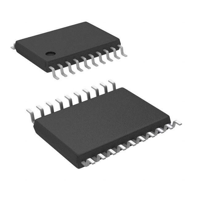
| 描述 | IC D-TYPE POS TRG SNGL 20TSSOP触发器 Octal D F/F w/Clear |
| 产品分类 | |
| 品牌 | STMicroelectronics |
| 产品手册 | http://www.st.com/st-web-ui/static/active/en/resource/technical/document/datasheet/CD00001785.pdf?s_searchtype=keyword |
| 产品图片 |
|
| rohs | 符合RoHS无铅 / 符合限制有害物质指令(RoHS)规范要求 |
| 产品系列 | 逻辑集成电路,触发器,STMicroelectronics 74LVX273TTR74LVX |
| 数据手册 | |
| 产品型号 | 74LVX273TTR |
| 不同V、最大CL时的最大传播延迟 | 14.5ns @ 3.3V, 50pF |
| 产品目录页面 | |
| 产品种类 | 触发器 |
| 传播延迟时间 | 20.4 ns |
| 低电平输出电流 | 4 mA |
| 元件数 | 1 |
| 其它名称 | 497-7116-1 |
| 其它有关文件 | http://www.st.com/web/catalog/sense_power/FM140/SC1798/PF62503?referrer=70071840 |
| 功能 | 主复位 |
| 包装 | 剪切带 (CT) |
| 商标 | STMicroelectronics |
| 安装类型 | 表面贴装 |
| 安装风格 | SMD/SMT |
| 封装 | Reel |
| 封装/外壳 | 20-TSSOP(0.173",4.40mm 宽) |
| 封装/箱体 | TSSOP-20 |
| 工作温度 | -55°C ~ 125°C (TA) |
| 工厂包装数量 | 2500 |
| 最大工作温度 | + 125 C |
| 最小工作温度 | - 55 C |
| 极性 | Non-Inverting |
| 标准包装 | 1 |
| 每元件位数 | 8 |
| 电压-电源 | 2 V ~ 3.6 V |
| 电流-输出高,低 | 4mA,4mA |
| 电流-静态 | 4µA |
| 电源电压-最大 | 3.6 V |
| 电源电压-最小 | 2 V |
| 电路数量 | 8 |
| 类型 | D 型 |
| 系列 | 74LVX273 |
| 触发器类型 | 正边沿 |
| 输入电容 | 5pF |
| 输入类型 | Single-Ended |
| 输入线路数量 | 8 |
| 输出类型 | 非反相 |
| 输出线路数量 | 8 |
| 逻辑类型 | D-Type Flip-Flop |
| 逻辑系列 | 74LV |
| 频率-时钟 | 90MHz |
| 高电平输出电流 | - 4 mA |


PDF Datasheet 数据手册内容提取
74LVX273 LOW VOLTAGE CMOS OCTAL D-TYPE FLIP-FLOP WITH CLEAR (5V TOLERANT INPUTS) (cid:1) HIGH SPEED: f = 150 MHz (TYP.) at V = 3.3V MAX CC (cid:1) 5V TOLERANT INPUTS (cid:1) POWER-DOWN PROTECTION ON INPUTS ) (cid:1) INPUT VOLTAGE LEVEL: s ( V = 0.8V, V = 2V at V =3V t IL IH CC c SOP TSSOP (cid:1) LOW POWER DISSIPATION: u I = 4 µA (MAX.) at T =25°C d CC A o (cid:1) LOW NOISE: Table 1: Order Codes r V = 0.3V (TYP.) at V =3.3V P OLP CC (cid:1) SYMMETRICAL OUTPUT IMPEDANCE: PACKAGE e T & R |IOH| = IOL = 4 mA (MIN) at VCC =3V SOP e t 74LVX273MTR (cid:1) BALANCED PROPAGATION DELAYS: TSSOPl 74LVX273TTR o t ≅ t PLH PHL s (cid:1) OPERATING VOLTAGE RANGE: b V (OPR) = 2V to 3.6V (1.2V Data Retention) transOferred to the Q outputs on the positive going CC edge of the clock pulse. (cid:1) PIN AND FUNCTION COMPATIBLE WITH -W hen the CLEAR input is held low, the Q outputs 74 SERIES 273 ) s are held low independently of the other inputs. (cid:1) IMPROVED LATCH-UP IMMUNITY ( Power down protection is provided on all inputs t c and 0 to 7V can be accepted on inputs with no DESCRIPTION u regard to the supply voltage. d The 74LVX273 is a low voltage CMOS OCTAL This device can be used to interface 5V to 3V. It o D-TYPE FLIP-FLOP WITH CLErAR fabricated with combines high speed performance with the true sub-micron silicon gate andP double-layer metal CMOS low power consumption. wiring C2MOS technoelo gy. It is ideal for low All inputs and outputs are equipped with power, battery opetrated and low noise 3.3V protection circuits against static discharge, giving e applications. them 2KV ESD immunity and transient excess l o Information signals applied to D inputs are voltage. s b O F igure 1: Pin Connection And IEC Logic Symbols Rev. 3 August 2004 1/12
74LVX273 Figure 2: Input Equivalent Circuit Table 2: Pin Description PIN N° SYMBOL NAME AND FUNCTION 1 CLEAR Asynchronous Master Reset (Active LOW) 2, 5, 6, 9, 12, Q0 to Q7 Flip-Flop Outputs 15, 16,19 3, 4, 7, 8, 13, D0 to D7 Data Inputs 14, 17, 18 11 CLOCK Clock Input (LOW-to-HIGH Edge Triggered) 10 GND Ground (0V) ) 20 V Positive Supply Voltage s CC ( t c Table 3: Truth Table u d o INPUTS OUTPUT r P FUNCTION CLEAR D B Q e L X X L CLEAR t e H L L l o H H s H b H X O Qn NO CHANGE X : Don’t Care - Figure 3: Logic Diagram s ) ( t c u d o r P e t e l o s b O This logic diagram has not be used to estimate propagation delays 2/12
74LVX273 Table 4: Absolute Maximum Ratings Symbol Parameter Value Unit VCC Supply Voltage -0.5 to +7.0 V VI DC Input Voltage -0.5 to +7.0 V VO DC Output Voltage -0.5 to VCC + 0.5 V IIK DC Input Diode Current - 20 mA IOK DC Output Diode Current ± 20 mA IO DC Output Current ± 25 mA ICC or IGND DC VCC or Ground Current ± 50 mA Tstg Storage Temperature -65 to +150 °C s ) TL Lead Temperature (10 sec) 300 t°C( c u Absolute Maximum Ratings are those values beyond which damage to the device may occur. Functional operation under these conditions is not implied d o Table 5: Recommended Operating Conditions r P Symbol Parameter e Value Unit t VCC Supply Voltage (note 1) e 2 to 3.6 V l VI Input Voltage o 0 to 5.5 V s VO Output Voltage b 0 to VCC V Top Operating Temperature O -55 to 125 °C dt/dv Input Rise and Fall Time (note 2) (VCC = 3V) - 0 to 100 ns/V ) 1) Truth Table guaranteed: 1.2V to 3.6V s 2) V from 0.8V to 2.0V ( IN t c Table 6: DC Specifications u d oTest Condition Value r P Symbol Parameter V TA = 25°C -40 to 85°C -55 to 125°C Unit CC e (V) Min. Typ. Max. Min. Max. Min. Max. t e V High Level Input 2.0 1.5 1.5 1.5 IH l o Voltage 3.0 2.0 2.0 2.0 V s b 3.6 2.4 2.4 2.4 O V Low Level Input 2.0 0.5 0.5 0.5 IL Voltage 3.0 0.8 0.8 0.8 V 3.6 0.8 0.8 0.8 VOH High Level Output 2.0 IO=-50 µA 1.9 2.0 1.9 1.9 Voltage 3.0 IO=-50 µA 2.9 3.0 2.9 2.9 V 3.0 IO=-4 mA 2.58 2.48 2.4 VOL Low Level Output 2.0 IO=50 µA 0.0 0.1 0.1 0.1 Voltage 3.0 IO=50 µA 0.0 0.1 0.1 0.1 V 3.0 IO=4 mA 0.36 0.44 0.55 I Input Leakage I Current 3.6 VI = 5V or GND ± 0.1 ± 1 ± 1 µA I Quiescent Supply CC Current 3.6 VI = VCC or GND 4 40 40 µA 3/12
74LVX273 Table 7: Dynamic Switching Characteristics Test Condition Value Symbol Parameter V TA = 25°C -40 to 85°C -55 to 125°C Unit CC (V) Min. Typ. Max. Min. Max. Min. Max. VOLP Dynamic Low Voltage 0.3 0.8 Quiet Output (note 1, 2) 3.3 VOLV -0.8 -0.3 VIHD DInypnuat m(nico tHe i1g,h 3 V)oltage 3.3 CL = 50 pF 2.0 V Dynamic Low Voltage VILD Input (note 1, 3) 3.3 0.8 ) s ( 1) Worst case package. t 2) Max number of outputs defined as (n). Data inputs are driven 0V to 3.3V, (n-1) outputs switching and one output at GND. c 3) Max number of data inputs (n) switching. (n-1) switching 0V to 3.3V. Inputs under test switching: 3.3V to threshold (V ), 0Vu to threshold ILD (VIHD), f=1MHz. d o Table 8: AC Electrical Characteristics (Input t = t = 3ns) r f r P Test Condition Valuee t Symbol Parameter V C TA = 25°C e-40 to 85°C -55 to 125°C Unit CC L l (V) (pF) o Min. Typ. sMax. Min. Max. Min. Max. b t Propagation Delay 2.7 15 9.0 16.9 1.0 20.5 1.0 22.0 PLH O tPHL Time 2.7 50 11.5 20.4 1.0 24.0 1.0 25.5 CK to Q 3.3(*) 15 - 7.1 11.0 1.0 13.0 1.0 14.5 ns ) 3.3(*) 50 s 9.6 14.5 1.0 16.5 1.0 18.0 ( tPHL Propagation Delay 3.3(*) 15 ct 9.3 17.6 1.0 20.5 1.0 22.0 TCiLmEeAR to Q 3.3(*) d50u 11.8 21.1 1.0 24.0 1.0 25.5 ns 5.0(o**) 15 7.3 11.5 1.0 13.5 1.0 15.5 P r5.0(**) 50 9.8 15.0 1.0 17.0 1.0 18.0 tW(L) CHLIGEHAR pulset Weid th, 32.3.7(*) 50 55..00 65..00 65..00 ns e tW CHLIsGOHCoKl pulse Width, 32.3.7(*) 50 55..50 65..50 65..50 ns b tSO SCeLtOupC KT imHIeG QH toor LOW 32.3.7(*) 50 54..55 64..55 64..55 ns Hold Time Q to 2.7 1.0 1.0 1.0 th CLOCK HIGH or LOW 3.3(*) 50 1.0 1.0 1.0 ns Recovery Time 2.7 2.5 2.5 2.5 tREM CLEAR to Q 3.3(*) 50 2.0 2.0 2.0 ns f Maximum Clock 2.7 15 55 110 55 50 MAX Frequency 2.7 50 45 60 40 35 MHz 3.3(*) 15 95 150 80 75 3.3(*) 50 60 90 55 50 tOSLH Output to Output 2.7 50 0.5 1.0 1.5 1.5 ns tOSHL Skew Time (note 1,2) 3.3(*) 50 0.5 1.0 1.5 1.5 1) Skew is defined as the absolute value of the difference between the actual propagation delay for any two outputs of the same device switch- ing in the same direction, either HIGH or LOW 2) Parameter guaranteed by design (*) Voltage range is 3.3V ± 0.3V 4/12
74LVX273 Table 4: CAPACITIVE CHARACTERISTICS Test Condition Value Symbol Parameter V TA = 25°C -40 to 85°C -55 to 125°C Unit CC (V) Min. Typ. Max. Min. Max. Min. Max. CIN Input Capacitance 3.3 5 10 10 10 pF C Power Dissipation PD Capacitance 3.3 fIN = 10MHz 40 pF (note 1) 1) C is defined as the value of the IC’s internal equivalent capacitance which is calculated from the operating current consumption without PD ad. (Refer to Test Circuit). Average operating current can be obtained by the following equation. I = C x V x f + I /8 (per circuit) CC(opr) PD CC IN CC ) Figure 5: Test Circuit s ( t c u d o r P e t e l o s b O - ) s ( t c u d C =15/50pF or equivalent (includes jig and porobe capacitance) RLT = ZOUT of pulse generator (typically 5r0Ω) P Figure 6: Waveform - Propagation Delays (f=1MHz; 50% duty cycle) e t e l o s b O 5/12
74LVX273 Figure 7: Waveform - Propagation Delays, Setup And Hold Times (f=1MHz; 50% duty cycle) ) s ( t c u d o r P e t e l o s b O - ) s ( t c u Figure 8: Waveform - Recovery Time (f=1MHz; 50% duty cycle) d o r P e t e l o s b O 6/12
74LVX273 SO-20 MECHANICAL DATA mm. inch DIM. MIN. TYP MAX. MIN. TYP. MAX. A 2.35 2.65 0.093 0.104 A1 0.1 0.30 0.004 0.012 B 0.33 0.51 0.013 0.020 ) C 0.23 0.32 0.009 0.013 s ( t D 12.60 13.00 0.496 0.5c12 u d E 7.4 7.6 0.291 0.299 o r e 1.27 0.05P0 e H 10.00 10.65 0.394 t 0.419 e l h 0.25 0.75 0.010o 0.030 s b L 0.4 1.27 0.016 0.050 O k 0° 8° - 0° 8° ) ddd s0.100 0.004 ( t c u d o r P e t e l o s b O 0016022D 7/12
74LVX273 TSSOP20 MECHANICAL DATA mm. inch DIM. MIN. TYP MAX. MIN. TYP. MAX. A 1.2 0.047 A1 0.05 0.15 0.002 0.004 0.006 A2 0.8 1 1.05 0.031 0.039 0.041 ) s ( b 0.19 0.30 0.007 0.012t c u c 0.09 0.20 0.004 d 0.0079 o r D 6.4 6.5 6.6 0.252 0.25P6 0.260 e E 6.2 6.4 6.6 0.244 0.252 0.260 t e E1 4.3 4.4 4.48 0.169ol 0.173 0.176 s e 0.65 BSC b 0.0256 BSC O K 0˚ 8˚ 0˚ 8˚ - ) L 0.45 0.60 s0.75 0.018 0.024 0.030 ( t c u d o r P A A2 e t e K L ol A1 b e c E s b O D E1 PIN 1 IDENTIFICATION 1 0087225C 8/12
74LVX273 Tape & Reel SO-20 MECHANICAL DATA mm. inch DIM. MIN. TYP MAX. MIN. TYP. MAX. A 330 12.992 C 12.8 13.2 0.504 0.519 D 20.2 0.795 ) N 60 2.362 s ( t T 30.4 1.1c97 u d Ao 10.8 11 0.425 0.433 o r Bo 13.2 13.4 0.520 P 0.528 Ko 3.1 3.3 0.122 e 0.130 t e Po 3.9 4.1 0.153 0.161 l o P 11.9 12.1 0s.468 0.476 b O - ) s ( t c u d o r P e t e l o s b O 9/12
74LVX273 Tape & Reel TSSOP20 MECHANICAL DATA mm. inch DIM. MIN. TYP MAX. MIN. TYP. MAX. A 330 12.992 C 12.8 13.2 0.504 0.519 D 20.2 0.795 ) N 60 2.362 s ( t T 22.4 0.8c82 u d Ao 6.8 7 0.268 0.276 o r Bo 6.9 7.1 0.272 P 0.280 Ko 1.7 1.9 0.067 e 0.075 t e Po 3.9 4.1 0.153 0.161 l o P 11.9 12.1 0s.468 0.476 b O - ) s ( t c u d o r P e t e l o s b O 10/12
74LVX273 Table 9: Revision History Date Revision Description of Changes 27-Aug-2004 3 Ordering Codes Revision - pag. 1. ) s ( t c u d o r P e t e l o s b O - ) s ( t c u d o r P e t e l o s b O 11/12
74LVX273 ) s ( t c u d o r P e t e l o s b O - ) s ( t c u d o r P e t e l o s b O Information furnished is believed to be accurate and reliable. However, STMicroelectronics assumes no responsibility for the consequences of use of such information nor for any infringement of patents or other rights of third parties which may result from its use. No license is granted by implication or otherwise under any patent or patent rights of STMicroelectronics. Specifications mentioned in this publication are subject to change without notice. This publication supersedes and replaces all information previously supplied. STMicroelectronics products are not authorized for use as critical components in life support devices or systems without express written approval of STMicroelectronics. The ST logo is a registered trademark of STMicroelectronics All other names are the property of their respective owners © 2004 STMicroelectronics - All Rights Reserved STMicroelectronics group of companies Australia - Belgium - Brazil - Canada - China - Czech Republic - Finland - France - Germany - Hong Kong - India - Israel - Italy - Japan - Malaysia - Malta - Morocco - Singapore - Spain - Sweden - Switzerland - United Kingdom - United States of America www.st.com 12/12