
 Datasheet下载
- 型号: 74LCX373WMX
- 制造商: Fairchild Semiconductor
- 库位|库存: xxxx|xxxx
- 要求:
| 数量阶梯 | 香港交货 | 国内含税 |
| +xxxx | $xxxx | ¥xxxx |
查看当月历史价格
查看今年历史价格
74LCX373WMX产品简介:
ICGOO电子元器件商城为您提供74LCX373WMX由Fairchild Semiconductor设计生产,在icgoo商城现货销售,并且可以通过原厂、代理商等渠道进行代购。 74LCX373WMX价格参考。Fairchild Semiconductor74LCX373WMX封装/规格:逻辑 - 锁销, D-Type Transparent Latch 1 Channel 8:8 IC Tri-State 20-SOIC。您可以下载74LCX373WMX参考资料、Datasheet数据手册功能说明书,资料中有74LCX373WMX 详细功能的应用电路图电压和使用方法及教程。
ON Semiconductor的74LCX373WMX是一款属于“逻辑 - 锁存器”类别的集成电路。具体来说,它是一个8位透明D型锁存器,带有三态输出。这种器件通常用于数据缓冲、信号调节和多路复用等应用场景。以下是其主要应用场景:

1. 数据缓冲与存储:
   74LCX373WMX可以用来临时存储数据信号。在数字系统中,当需要将数据从一个时钟域传递到另一个时钟域时,透明锁存器可以起到桥梁作用,确保数据在适当的时刻被捕获和保持。

2. 总线控制:
   由于该芯片具有三态输出功能,它可以方便地用于多主设备共享同一数据总线的场景。通过启用或禁用输出,多个设备可以在同一总线上通信而不发生冲突。

3. 信号同步:
   在异步数字电路中,透明锁存器可以帮助同步不同来源的信号。例如,在复杂的嵌入式系统中,可能需要将来自外部传感器或接口的数据与内部时钟同步。

4. 地址锁存:
   在微处理器或微控制器系统中,74LCX373WMX可以用作地址锁存器,将地址信息从地址/数据总线分离出来,以便后续访问存储器或其他外设。

5. 多路复用与解复用:
   结合其他逻辑器件,74LCX373WMX可用于构建多路复用器或多路解复用器,从而减少所需的物理连接数量并优化系统设计。

6. 工业自动化与控制:
   在工业环境中,这款芯片可以用于输入/输出端口扩展,或者作为中间级来管理复杂控制系统中的信号流。

总之,74LCX373WMX适用于各种需要高效数据管理和信号处理的应用场合,特别是在对速度和功耗有较高要求的现代电子系统中。
| 参数 | 数值 |
| 产品目录 | 集成电路 (IC)半导体 |
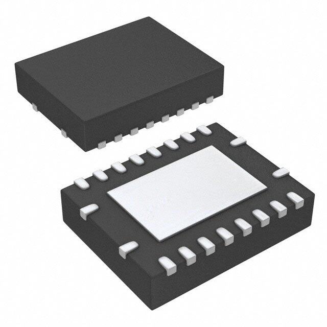
| 描述 | IC LATCH TRANSP OCT LV 20SOIC闭锁 Octal Trans Latch |
| 产品分类 | |
| 品牌 | Fairchild Semiconductor |
| 产品手册 | |
| 产品图片 |
|
| rohs | 符合RoHS无铅 / 符合限制有害物质指令(RoHS)规范要求 |
| 产品系列 | 逻辑集成电路,闭锁,Fairchild Semiconductor 74LCX373WMX74LCX |
| 数据手册 | |
| 产品型号 | 74LCX373WMX |
| 产品种类 | 闭锁 |
| 传播延迟时间 | 9 ns at 2.7 V, 8 ns at 3.3 V |
| 供应商器件封装 | 20-SOIC |
| 其它名称 | 74LCX373WMXCT |
| 包装 | 剪切带 (CT) |
| 单位重量 | 801 mg |
| 商标 | Fairchild Semiconductor |
| 安装类型 | 表面贴装 |
| 安装风格 | SMD/SMT |
| 封装 | Reel |
| 封装/外壳 | 20-SOIC(0.295",7.50mm 宽) |
| 封装/箱体 | SOIC-20 |
| 工作温度 | -40°C ~ 85°C |
| 工厂包装数量 | 1000 |
| 延迟时间-传播 | 1.5ns |
| 最大工作温度 | + 85 C |
| 最小工作温度 | - 40 C |
| 极性 | Non-Inverting |
| 标准包装 | 1 |
| 独立电路 | 1 |
| 电压-电源 | 2 V ~ 3.6 V |
| 电流-输出高,低 | 24mA,24mA |
| 电源电压-最大 | 3.6 V |
| 电源电压-最小 | 2 V |
| 电路 | 8:8 |
| 电路数量 | 8 Circuit |
| 系列 | 74LCX373 |
| 输入线路数量 | 2 Line |
| 输出类型 | 三态 |
| 输出线路数量 | 3 Line |
| 逻辑类型 | Transparent Latch |
| 逻辑系列 | 74LC |
| 零件号别名 | 74LCX373WMX_NL |
| 高电平输出电流 | - 24 mA |


- 商务部:美国ITC正式对集成电路等产品启动337调查
- 曝三星4nm工艺存在良率问题 高通将骁龙8 Gen1或转产台积电
- 太阳诱电将投资9.5亿元在常州建新厂生产MLCC 预计2023年完工
- 英特尔发布欧洲新工厂建设计划 深化IDM 2.0 战略
- 台积电先进制程称霸业界 有大客户加持明年业绩稳了
- 达到5530亿美元!SIA预计今年全球半导体销售额将创下新高
- 英特尔拟将自动驾驶子公司Mobileye上市 估值或超500亿美元
- 三星加码芯片和SET,合并消费电子和移动部门,撤换高东真等 CEO
- 三星电子宣布重大人事变动 还合并消费电子和移动部门
- 海关总署:前11个月进口集成电路产品价值2.52万亿元 增长14.8%


PDF Datasheet 数据手册内容提取
7 4 L C February 2008 X 3 7 3 — 74LCX373 L o Low Voltage Octal Transparent Latch w V o with 5V Tolerant Inputs and Outputs l t a g e Features General Description O c ■ 5V tolerant inputs and outputs The LCX373 consists of eight latches with 3-STATE t a ■ 2.3V–3.6V VCC specifications provided outputs for bus organized system applications. The l T ■ 8.0ns tPD max. (VCC = 3.3V), 10µA ICC max. device is designed for low voltage applications with ra capability of interfacing to a 5V signal environment. n ■ Power down high impedance inputs and outputs s ■ Supports live insertion/withdrawal(1) The LCX373 is fabricated with an advanced CMOS p a ■ ±24mA output drive (VCC = 3.0V) tteacinhinngo loCgMyO toS alocwhi epvoew ehrig dhi ssspipeaetdio onp.eration while main- ren ■ Implements patented noise/EMI reduction circuitry t ■ Latch-up performance exceeds JEDEC 78 conditions L a ■ ESD performance tc – Human body model > 2000V h w – Machine model > 200V i t ■ Leadless DQFN package h 5 V Note: T o 1. To ensure the high impedance state during power up l e or down, OE should be tied to VCC through a pull-up ra resistor: the minimum value of the resistor is n determined by the current-sourcing capability of the t I driver. n p u t s a Ordering Information n d Order Package O u Number Number Package Description t p 74LCX373WM M20B 20-Lead Small Outline Integrated Circuit (SOIC), JEDEC MS-013, 0.300" Wide u t s 74LCX373SJ M20D 20-Lead Small Outline Package (SOP), EIAJ TYPE II, 5.3mm Wide 74LCX373BQX(2) MLP20B 20-Terminal Depopulated Quad Very-Thin Flat Pack No Leads (DQFN), JEDEC MO-241, 2.5 x 4.5mm 74LCX373MSA MSA20 20-Lead Shrink Small Outline Package (SSOP), JEDEC MO-150, 5.3mm Wide 74LCX373MTC MTC20 20-Lead Thin Shrink Small Outline Package (TSSOP), JEDEC MO-153, 4.4mm Wide Note: 2. DQFN package available in Tape and Reel only. Device also available in Tape and Reel. Specify by appending suffix letter “X” to the ordering number. All packages are lead free per JEDEC: J-STD-020B standard. ©2006 Fairchild Semiconductor Corporation www.fairchildsemi.com 74LCX373 Rev. 1.8.0
7 4 Connection Diagrams Logic Symbols L C X Pin Assignments for 3 SOIC, SOP, SSOP, TSSOP 7 D0D1D2D3D4D5D6D7 3 LE — OE 1 20 VCC OE L O0 2 19 O7 O0O1O2O3O4O5O6O7 o D0 3 18 D7 w D1 4 17 D6 V O1 5 16 O6 IEEE/IEC ol O2 6 15 O5 ta D2 7 14 D5 OLEE ECN1 ge D3 8 13 D4 O GNOD3 910 1121 OLE4 DD01 1D OO01 ctal D2 O2 Tr D3 O3 an Pad Assignments for DQFN D4 O4 s OE VCC D5 O5 pa 1 20 D6 O6 re D7 O7 n O0 2 19 O7 t L D0 3 18 D7 a t D1 4 17 D6 Truth Table ch w O1 5 16 O6 Inputs Outputs i t O2 6 15 O5 LE OE Dn On h 5 D2 7 14 D5 X H X Z V T D3 8 13 D4 H L L L o l e O3 9 12 O4 H L H H r a n 10 11 L L X O 0 t GND LE I H = HIGH Voltage n p (Top View) L = LOW Voltage u t s Pin Descriptions Z = High Impedance a X = Immaterial n Pin Names Description d O0 = Previous O0 before HIGH-to-LOW transition O D0–D7 Data Inputs of Latch Enable u t LE Latch Enable Input p u OE 3-STATE Output Enable Input Functional Description ts O –O 3-STATE Latch Outputs 0 7 The LCX373 contains eight D-type latches with 3-STATE standard outputs. When the Latch Enable (LE) input is HIGH, data on the D inputs enters the latches. In this n condition the latches are transparent, i.e. a latch output will change state each time its D input changes. When LE is LOW, the latches store the information that was present on the D inputs a setup time preceding the HIGH-to-LOW transition of LE. The 3-STATE standard outputs are controlled by the Output Enable (OE) input. When OE is LOW, the standard outputs are in the 2-state mode. When OE is HIGH, the standard outputs are in the high impedance mode but this does not inter- fere with entering new data into the latches. ©2006 Fairchild Semiconductor Corporation www.fairchildsemi.com 74LCX373 Rev. 1.8.0 2
7 4 Logic Diagram L C X D0 D1 D2 D3 D4 D5 D6 D7 3 7 3 D D D D D D D D — L O O O O O O O O o G G G G G G G G w V LE o l t a g e O OE c t O0 O1 O2 O3 O4 O5 O6 O7 al T Please note that this diagram is provided only for the understanding of logic operations and should not be used to ra estimate propagation delays. n s p a r e n t L a t c h w i t h 5 V T o l e r a n t I n p u t s a n d O u t p u t s ©2006 Fairchild Semiconductor Corporation www.fairchildsemi.com 74LCX373 Rev. 1.8.0 3
7 4 Absolute Maximum Ratings L C Stresses exceeding the absolute maximum ratings may damage the device. The device may not function or be X 3 operable above the recommended operating conditions and stressing the parts to these levels is not recommended. 7 In addition, extended exposure to stresses above the recommended operating conditions may affect device reliability. 3 The absolute maximum ratings are stress ratings only. — L Symbol Parameter Conditions Value Units o w VCC Supply Voltage –0.5 to +7.0 V V V DC Input Voltage –0.5 to +7.0 V o I l t a V DC Output Voltage Output in 3-STATE –0.5 to +7.0 V O g Output in HIGH or LOW State(3) –0.5 to VCC + 0.5 e O I DC Input Diode Current V < GND –50 mA c IK I t IOK DC Output Diode Current VO < GND –50 mA al T V > V +50 r O CC a n I DC Output Source/Sink Current ±50 mA O s p ICC DC Supply Current per Supply Pin ±100 mA a r I DC Ground Current per Ground Pin ±100 mA e GND n TSTG Storage Temperature –65 to +150 °C t L a t c h Recommended Operating Conditions(4) w The Recommended Operating Conditions table defines the conditions for actual device operation. Recommended it h operating conditions are specified to ensure optimal performance to the datasheet specifications. Fairchild does not 5 recommend exceeding them or designing to absolute maximum ratings. V T Symbol Parameter Conditions Min. Max. Units o l e VCC Supply Voltage Operating 2.0 3.6 V ra Data Retention 1.5 3.6 n t VI Input Voltage 0 5.5 V In p VO Output Voltage HIGH or LOW State 0 VCC V u t 3-STATE 0 5.5 s a I /I Output Current V = 3.0V–3.6V ±24 mA n OH OL CC d VCC = 2.7V–3.0V ±12 O u V = 2.3V–2.7V ±8 CC t p T Free-Air Operating Temperature –40 85 °C u A t ∆t/∆V Input Edge Rate V = 0.8V–2.0V, V = 3.0V 0 10 ns/V s IN CC Notes: 3. I Absolute Maximum Rating must be observed. O 4. Unused inputs must be held HIGH or LOW. They may not float. ©2006 Fairchild Semiconductor Corporation www.fairchildsemi.com 74LCX373 Rev. 1.8.0 4
7 4 DC Electrical Characteristics L C T = –40°C to +85°C X A 3 7 Symbol Parameter V (V) Conditions Min. Max. Units CC 3 V HIGH Level Input Voltage 2.3–2.7 1.7 V — IH 2.7–3.6 2.0 L o V LOW Level Input Voltage 2.3–2.7 0.7 V w IL V 2.7–3.6 0.8 o l t V HIGH Level Output Voltage 2.3–3.6 I = –100µA V – 0.2 V a OH OH CC g 2.3 I = –8mA 1.8 e OH O 2.7 I = –12mA 2.2 OH c t 3.0 I = –18mA 2.4 a OH l T 3.0 IOH = –24mA 2.2 r a V LOW Level Output Voltage 2.3–3.6 I = 100µA 0.2 V n OL OL s 2.3 I = 8mA 0.6 p OL a 2.7 IOL = 12mA 0.4 re n 3.0 IOL = 16mA 0.4 t L 3.0 I = 24mA 0.55 a OL t II Input Leakage Current 2.3–3.6 0 ≤ VI ≤ 5.5V ±5.0 µA ch I 3-STATE Output Leakage 2.3–3.6 0 ≤ V ≤ 5.5V, ±5.0 µA w OZ O i V = V or V t I IH IL h I Power-Off Leakage Current 0 V or V = 5.5V 10 µA 5 OFF I O V ICC Quiescent Supply Current 2.3–3.6 VI = VCC or GND 10 µA T o 2.3–3.6 3.6V ≤ V, V ≤ 5.5V(5) ±10 l I O e ∆I Increase in I per Input 2.3–3.6 V = V –0.6V 500 µA ra CC CC IH CC n t I n p u AC Electrical Characteristics t s a TA = –40°C to +85°C, RL = 500Ω n d V = 3.3V ± 0.3V, V = 2.7V, V = 2.5 ± 0.2V, CC CC CC O CL = 50pF CL = 50pF CL = 30pF u t Symbol Parameter Min. Max. Min. Max. Min. Max. Units p u t t , t Propagation Delay, D to O 1.5 8.0 1.5 9.0 1.5 9.6 ns s PHL PLH n n t , t Propagation Delay, LE to O 1.5 8.5 1.5 9.5 1.5 10.5 ns PHL PLH n t , t Output Enable Time 1.5 8.5 1.5 9.5 1.5 10.5 ns PZL PZH t , t Output Disable Time 1.5 7.5 1.5 8.5 1.5 9.0 ns PLZ PHZ t Setup Time, D to LE 2.5 2.5 4.0 ns S n t Hold Time, D to LE 1.5 1.5 2.0 ns H n t LE Pulse Width 3.3 3.3 4.0 ns W t t Output to Output Skew(6) 1.0 ns OSHL, OSLH Notes: 5. Outputs disabled or 3-STATE only. 6. Skew is defined as the absolute value of the difference between the actual propagation delay for any two separate outputs of the same device. The specification applies to any outputs switching in the same direction, either HIGH-to-LOW (t ) or LOW-to-HIGH (t ). OSHL OSLH ©2006 Fairchild Semiconductor Corporation www.fairchildsemi.com 74LCX373 Rev. 1.8.0 5
7 4 Dynamic Switching Characteristics L C X T = 25°C 3 A 7 3 Symbol Parameter V (V) Conditions Typical Units CC — VOLP Quiet Output Dynamic Peak VOL 3.3 CL = 50pF, VIH = 3.3V, VIL = 0V 0.8 V L 2.5 C = 30pF, V = 2.5V, V = 0V 0.6 o L I IL w VOLV Quiet Output Dynamic Valley VOL 3.3 CL = 50pF, VIH = 3.3V, VIL = 0V –0.8 V V o 2.5 CL = 30pF, VI = 2.5V, VIL = 0V –0.6 lt a g e Capacitance O c t a Symbol Parameter Conditions Typical Units l T CIN Input Capacitance VCC = Open, VI = 0V or VCC 7 pF ra n COUT Output Capacitance VCC = 3.3V, VI = 0V or VCC 8 pF s p C Power Dissipation Capacitance V = 3.3V, V = 0V or V , f = 10MHz 25 pF a PD CC I CC r e n t L a t c h w i t h 5 V T o l e r a n t I n p u t s a n d O u t p u t s ©2006 Fairchild Semiconductor Corporation www.fairchildsemi.com 74LCX373 Rev. 1.8.0 6
7 4 AC Loading and Waveforms (Generic for LCX Family) LC X 3 VCC 7 500Ω OPEN tPLH, tPHL 3 TEST DUT GND tPZH, tPHZ — SIGNAL VI tPZL, tPLZ L CL 500Ω o w V o l Figure 1. AC Test Circuit (C includes probe and jig capacitance) t L a g e Test Switch O t , t Open c PLH PHL t a t , t 6V at V = 3.3 ± 0.3V l PZL PLZ CC T VCC x 2 at VCC = 2.5 ± 0.2V ra t , t GND n PZH PHZ s p a DATINA Vmi VGCNCD COONUTTRPOUTL Vmi VGCNCD ren tpxx tpxx tPZH tPHZ t L DOAUTAT Vmo DOAUTAT Vmo VVOYH at c h Waveform for Inverting and 3-STATE Output High Enable and w Non-Inverting Functions Disable Times for Logic it h 5 COCNLTORCOINKL tW treVcmiVmi VGCNCD CONINTDRPAOUTITLNA tS VtHmi Vmi VGVGCCNNCCDD V Toleran tPHL tPLH MR tS trec t I OR Vmi n OUTPUT Vmo Vmo CLEAR p u t s Propagation Delay, Pulse Width and Setup Time, Hold Time and a t Waveforms Recovery Time for Logic n rec d O COONUTTRPOUTL Vmi VGCNCD tr tf utp tPZL tPLZ VOH u DOAUTAT Vmo VX OUTAPNUYT 10%90% 90%10% ts VOL VOL t and t 3-STATE Output Low Enable and rise fall Disable Times for Logic Figure 2. Waveforms (Input Characteristics; f = 1MHz, t = t = 3ns) r f V CC Symbol 3.3V ± 0.3V 2.7V 2.5V ± 0.2V V 1.5V 1.5V V / 2 mi CC V 1.5V 1.5V V / 2 mo CC V V + 0.3V V + 0.3V V + 0.15V x OL OL OL V V – 0.3V V – 0.3V V – 0.15V y OH OH OH ©2006 Fairchild Semiconductor Corporation www.fairchildsemi.com 74LCX373 Rev. 1.8.0 7
7 4 Schematic Diagram (Generic for LCX Family) LC X Input Stage 3 7 3 — L o P2 w V P1 o l VCC ta g e O Data c t ESD a P5 X1 l T D2 N+/P– VDD ra N1 N2 n s p a GTO™ Output r e Input Stage n t P4 D6 L N+/P– a t c h w i t h P3 5 V N5 T o l e Enable r N4 a ESD n t D4 N+/P– I n N3 p u t s a n d O u t p u t s ©2006 Fairchild Semiconductor Corporation www.fairchildsemi.com 74LCX373 Rev. 1.8.0 8
7 4 Tape and Reel Specification L C X Tape Format for DQFN 3 7 Package Tape Number Cavity Cover Tape 3 — Designator Section Cavities Status Status L BQX Leader (Start End) 125 (typ) Empty Sealed o w Carrier 3000 Filled Sealed V Trailer (Hub End) 75 (typ) Empty Sealed o l t a Tape Dimensions inches (millimeters) g e O c t a l T r a n s p a r e n t L a t c h w i t h 5 V T o l e r a n t I n p u t s a n d O u Reel Dimensions inches (millimeters) tp u t s Tape Size A B C D N W1 W2 12mm 13.0 (330.0) 0.059 (1.50) 0.512 (13.00) 0.795 (20.20) 2.165 (55.00) 0.488 (12.4) 0.724 (18.4) ©2006 Fairchild Semiconductor Corporation www.fairchildsemi.com 74LCX373 Rev. 1.8.0 9
7 4 Physical Dimensions L C X 3 13.00 7 12.60 3 A — 11.43 L 20 11 o B w V o l t a 9.50 g e 10.65 7.60 10.00 7.40 O c t 2.25 a l T r a n s 1 10 0.65 p PINONE 0.51 1.27 1.27 a INDICATOR 0.35 re 0.25 M C B A n t LANDPATTERNRECOMMENDATION L a t c 2.65MAX SEEDETAILA h w i 0.33 th C 0.20 5 V 0.30 0.10 C T 0.75 0.10 SEATINGPLANE o 0.25X45° le NOTES:UNLESSOTHERWISESPECIFIED r a n (R0.10) A) THISPACKAGECONFORMSTOJEDEC t (R0.10) GAGEPLANE MS-013,VARIATIONAC,ISSUEE In p 80°° 0.25 BC)) ADLIMLEDNIMSEIONNSSIODNOSNAORTEIINNCMLUILDLIEMMETOELRDS. uts FLASHORBURRS. a 1.27 D) CONFORMSTOASMEY14.5M-1994 n 0.40 SEATINGPLANE E) LANDPATTERNSTANDARD:SOIC127P1030X265-20L d O (1.40) DETAILA F) DRAWINGFILENAME:MKT-M20BREV3 u SCALE:2:1 tp u t Figure 3. 20-Lead Small Outline Integrated Circuit (SOIC), JEDEC MS-013, 0.300" Wide s Package drawings are provided as a service to customers considering Fairchild components. Drawings may change in any manner without notice. Please note the revision and/or date on the drawing and contact a Fairchild Semiconductor representative to verify or obtain the most recent revision. Package specifications do not expand the terms of Fairchild’s worldwide terms and conditions, specifically the warranty therein, which covers Fairchild products. Always visit Fairchild Semiconductor’s online packaging area for the most recent package drawings: http://www.fairchildsemi.com/packaging/ ©2006 Fairchild Semiconductor Corporation www.fairchildsemi.com 74LCX373 Rev. 1.8.0 10
7 4 Physical Dimensions (Continued) LC X 3 7 3 — L o w V o l t a g e O c t a l T r a n s p a r e n t L a t c h w i t h 5 V T o l e r a n t I n p u t s a n d O u t p u t s Figure 4. 20-Lead Small Outline Package (SOP), EIAJ TYPE II, 5.3mm Wide Package drawings are provided as a service to customers considering Fairchild components. Drawings may change in any manner without notice. Please note the revision and/or date on the drawing and contact a Fairchild Semiconductor representative to verify or obtain the most recent revision. Package specifications do not expand the terms of Fairchild’s worldwide terms and conditions, specifically the warranty therein, which covers Fairchild products. Always visit Fairchild Semiconductor’s online packaging area for the most recent package drawings: http://www.fairchildsemi.com/packaging/ ©2006 Fairchild Semiconductor Corporation www.fairchildsemi.com 74LCX373 Rev. 1.8.0 11
7 4 Physical Dimensions (Continued) LC X 3 7 3 — L o w V o l t a g e O c t a l T r a n s p a r e n t L a t c h w i t h 5 V T o l e r a n t I n p u t s a n d O u t p u t s Figure 5. 20-Terminal Depopulated Quad Very-Thin Flat Pack No Leads (DQFN), JEDEC MO-241, 2.5 x 4.5mm Package drawings are provided as a service to customers considering Fairchild components. Drawings may change in any manner without notice. Please note the revision and/or date on the drawing and contact a Fairchild Semiconductor representative to verify or obtain the most recent revision. Package specifications do not expand the terms of Fairchild’s worldwide terms and conditions, specifically the warranty therein, which covers Fairchild products. Always visit Fairchild Semiconductor’s online packaging area for the most recent package drawings: http://www.fairchildsemi.com/packaging/ ©2006 Fairchild Semiconductor Corporation www.fairchildsemi.com 74LCX373 Rev. 1.8.0 12
7 4 Physical Dimensions (Continued) LC X 3 7 3 — L o w V o l t a g e O c t a l T r a n s p a r e n t L a t c h w i t h 5 V T o l e r a n t I n p u t s a n d O u t p u t s Figure 6. 20-Lead Shrink Small Outline Package (SSOP), JEDEC MO-150, 5.3mm Wide Package drawings are provided as a service to customers considering Fairchild components. Drawings may change in any manner without notice. Please note the revision and/or date on the drawing and contact a Fairchild Semiconductor representative to verify or obtain the most recent revision. Package specifications do not expand the terms of Fairchild’s worldwide terms and conditions, specifically the warranty therein, which covers Fairchild products. Always visit Fairchild Semiconductor’s online packaging area for the most recent package drawings: http://www.fairchildsemi.com/packaging/ ©2006 Fairchild Semiconductor Corporation www.fairchildsemi.com 74LCX373 Rev. 1.8.0 13
7 4 Physical Dimensions (Continued) LC X 3 7 3 — L o w V o l t a g e O c t a l T r a n s p a r e n t L a t c h w i t h 5 V T o l e r a n t I n p u t s a n d O u t p u t s Figure 7. 20-Lead Thin Shrink Small Outline Package (TSSOP), JEDEC MO-153, 4.4mm Wide Package drawings are provided as a service to customers considering Fairchild components. Drawings may change in any manner without notice. Please note the revision and/or date on the drawing and contact a Fairchild Semiconductor representative to verify or obtain the most recent revision. Package specifications do not expand the terms of Fairchild’s worldwide terms and conditions, specifically the warranty therein, which covers Fairchild products. Always visit Fairchild Semiconductor’s online packaging area for the most recent package drawings: http://www.fairchildsemi.com/packaging/ ©2006 Fairchild Semiconductor Corporation www.fairchildsemi.com 74LCX373 Rev. 1.8.0 14
7 4 L C X 3 7 3 — TRADEMARKS L Thefollowingincludesregisteredandunregisteredtrademarksandservicemarks,ownedbyFairchildSemiconductorand/oritsglobal o subsidiaries,andisnotintendedtobeanexhaustivelistofallsuchtrademarks. w ACEx® FPS™ PDP-SPM™ SupreMOS™ V BuilditNow™ FRFET® Power220® SyncFET™ ol CorePLUS™ GlobalPowerResourceSM POWEREDGE® ® ta CROSSVOLT™ GreenFPS™ Power-SPM™ ThePowerFranchise® g CTL™ GreenFPS™e-Series™ PowerTrench® e O CurrentTransferLogic™ GTO™ ProgrammableActiveDroop™ EcoSPARK® i-Lo™ QFET® TinyBoost™ ct EZSWITCH™* IntelliMAX™ QS™ TinyBuck™ al ™ ISOPLANAR™ QTOptoelectronics™ TinyLogic® T r MegaBuck™ QuietSeries™ TINYOPTO™ a ® MICROCOUPLER™ RapidConfigure™ TinyPower™ n s Fairchild® MicroFET™ SMARTSTART™ TinyPWM™ p FairchildSemiconductor® MicroPak™ SPM® TinyWire™ a FACTQuietSeries™ MillerDrive™ STEALTH™ µSerDes™ re FACT® Motion-SPM™ SuperFET™ UHC® n FAST® OPTOLOGIC® SuperSOT™-3 UltraFRFET™ t L FastvCore™ OPTOPLANAR® SuperSOT™-6 UniFET™ a FlashWriter®* ® SuperSOT™-8 VCX™ tc h *EZSWITCH™andFlashWriter®aretrademarksofSystemGeneralCorporation,usedunderlicensebyFairchildSemiconductor. w i t h DISCLAIMER 5 FAIRCHILDSEMICONDUCTORRESERVESTHERIGHTTOMAKECHANGESWITHOUTFURTHERNOTICETOANYPRODUCTS V HEREINTOIMPROVERELIABILITY,FUNCTION,ORDESIGN.FAIRCHILDDOESNOTASSUMEANYLIABILITYARISINGOUTOFTHE T o APPLICATIONORUSEOFANYPRODUCTORCIRCUITDESCRIBEDHEREIN;NEITHERDOESITCONVEYANYLICENSEUNDERITS l PATENTRIGHTS,NORTHERIGHTSOFOTHERS.THESESPECIFICATIONSDONOTEXPANDTHETERMSOFFAIRCHILD’S e r WORLDWIDETERMSANDCONDITIONS,SPECIFICALLYTHEWARRANTYTHEREIN,WHICHCOVERSTHESEPRODUCTS. a n t I LIFESUPPORTPOLICY n p FAIRCHILD’SPRODUCTSARENOTAUTHORIZEDFORUSEASCRITICALCOMPONENTSINLIFESUPPORTDEVICESOR u SYSTEMSWITHOUTTHEEXPRESSWRITTENAPPROVALOFFAIRCHILDSEMICONDUCTORCORPORATION. t s Asusedherein: a n 1. Life support devices or systems are devices or systems 2. A critical component in any component of a life support, d which, (a) are intended for surgical implant intothebodyor device, or system whose failure to perform can be O (b) support or sustain life, and (c) whose failure to perform reasonablyexpectedtocausethefailureofthelifesupport u when properly used in accordance with instructions for use deviceorsystem,ortoaffectitssafetyoreffectiveness. t provided in the labeling, can be reasonably expected to p u resultinasignificantinjuryoftheuser. t s PRODUCTSTATUSDEFINITIONS DefinitionofTerms DatasheetIdentification ProductStatus Definition Thisdatasheetcontainsthedesignspecificationsforproduct AdvanceInformation FormativeorInDesign development.Specificationsmaychangeinanymannerwithoutnotice. Thisdatasheetcontainspreliminarydata;supplementarydatawillbe Preliminary First Production publishedatalaterdate.FairchildSemiconductorreservestherightto makechangesatanytimewithoutnoticetoimprovedesign. Thisdatasheetcontainsfinalspecifications.FairchildSemiconductor NoIdentificationNeeded FullProduction reservestherighttomakechangesatanytimewithoutnoticetoimprove thedesign. Thisdatasheetcontainsspecificationsonaproductthathasbeen Obsolete NotInProduction discontinuedbyFairchildSemiconductor.Thedatasheetisprintedfor referenceinformationonly. Rev.I33 ©2006 Fairchild Semiconductor Corporation www.fairchildsemi.com 74LCX373 Rev. 1.8.0 15