ICGOO在线商城 > 集成电路(IC) > 逻辑 - 栅极和逆变器 > 74LCX32BQX
 Datasheet下载
- 型号: 74LCX32BQX
- 制造商: Fairchild Semiconductor
- 库位|库存: xxxx|xxxx
- 要求:
| 数量阶梯 | 香港交货 | 国内含税 |
| +xxxx | $xxxx | ¥xxxx |
查看当月历史价格
查看今年历史价格
74LCX32BQX产品简介:
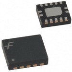
ICGOO电子元器件商城为您提供74LCX32BQX由Fairchild Semiconductor设计生产,在icgoo商城现货销售,并且可以通过原厂、代理商等渠道进行代购。 74LCX32BQX价格参考。Fairchild Semiconductor74LCX32BQX封装/规格:逻辑 - 栅极和逆变器, OR Gate IC 4 Channel 14-DQFN (3x2.5)。您可以下载74LCX32BQX参考资料、Datasheet数据手册功能说明书,资料中有74LCX32BQX 详细功能的应用电路图电压和使用方法及教程。
74LCX32BQX 是安森美半导体(ON Semiconductor)生产的一款逻辑门器件,属于四路2输入或门(Quad 2-Input OR Gate)。该器件属于74LCX系列,具有低电压、低功耗和高传输速率的特点,适用于需要高效能逻辑运算的数字电路设计。

主要应用场景包括:

1. 数字信号处理系统:用于执行基本的逻辑“或”运算,广泛应用于数据路径控制、状态判断等场景。
2. 通信设备:在通信模块中作为基础逻辑元件,用于地址解码、中断请求合并等功能。
3. 工业控制系统:用于PLC、传感器信号整合与控制逻辑实现。
4. 消费电子产品:如智能家电、穿戴设备中,用于简化逻辑控制电路。
5. 嵌入式系统:在微控制器外围电路中实现逻辑组合功能,扩展控制能力。
6. 测试测量仪器:用于逻辑分析仪、信号发生器中的信号合成与处理。

该器件采用小型封装(如TSSOP),适合高密度PCB布局,并支持宽温度范围,适应工业级应用需求。
| 参数 | 数值 |
| 产品目录 | 集成电路 (IC)半导体 |
| 描述 | IC GATE OR 4CH 2-INP 14-DQFN逻辑门 Quad 2-Input OR Gate with 5V Tolerant |
| 产品分类 | |
| 品牌 | Fairchild Semiconductor |
| 产品手册 | |
| 产品图片 |
|
| rohs | 符合RoHS无铅 / 符合限制有害物质指令(RoHS)规范要求 |
| 产品系列 | 逻辑集成电路,逻辑门,Fairchild Semiconductor 74LCX32BQX74LCX |
| 数据手册 | |
| 产品型号 | 74LCX32BQX |
| 不同V、最大CL时的最大传播延迟 | 5.5ns @ 3.3V,50pF |
| 产品 | OR |
| 产品目录页面 | |
| 产品种类 | 逻辑门 |
| 传播延迟时间 | 6.2 ns |
| 低电平输出电流 | 24 mA |
| 供应商器件封装 | 14-DQFN(3x2.5) |
| 其它名称 | 74LCX32BQX-ND |
| 包装 | 带卷 (TR) |
| 单位重量 | 120 mg |
| 商标 | Fairchild Semiconductor |
| 安装类型 | 表面贴装 |
| 安装风格 | SMD/SMT |
| 封装 | Reel |
| 封装/外壳 | 14-WFQFN 裸露焊盘 |
| 封装/箱体 | DQFN |
| 工作温度 | -40°C ~ 85°C |
| 工厂包装数量 | 3000 |
| 最大工作温度 | + 85 C |
| 最小工作温度 | - 40 C |
| 栅极数量 | 4 Gate |
| 标准包装 | 3,000 |
| 特性 | - |
| 电压-电源 | 2 V ~ 3.6 V |
| 电流-输出高,低 | 24mA,24mA |
| 电流-静态(最大值) | 10µA |
| 电源电压-最大 | 3.6 V |
| 电源电压-最小 | 2 V |
| 电路数 | 4 |
| 系列 | 74LCX32 |
| 输入/输出线数量 | 2 / 1 |
| 输入数 | 2 |
| 输入线路数量 | 2 |
| 输出线路数量 | 1 |
| 逻辑电平-低 | 0.7 V ~ 0.8 V |
| 逻辑电平-高 | 1.7 V ~ 2 V |
| 逻辑类型 | 或门 |
| 逻辑系列 | 74LCX |
| 高电平输出电流 | - 24 mA |


- 商务部:美国ITC正式对集成电路等产品启动337调查
- 曝三星4nm工艺存在良率问题 高通将骁龙8 Gen1或转产台积电
- 太阳诱电将投资9.5亿元在常州建新厂生产MLCC 预计2023年完工
- 英特尔发布欧洲新工厂建设计划 深化IDM 2.0 战略
- 台积电先进制程称霸业界 有大客户加持明年业绩稳了
- 达到5530亿美元!SIA预计今年全球半导体销售额将创下新高
- 英特尔拟将自动驾驶子公司Mobileye上市 估值或超500亿美元
- 三星加码芯片和SET,合并消费电子和移动部门,撤换高东真等 CEO
- 三星电子宣布重大人事变动 还合并消费电子和移动部门
- 海关总署:前11个月进口集成电路产品价值2.52万亿元 增长14.8%


PDF Datasheet 数据手册内容提取
Is Now Part of To learn more about ON Semiconductor, please visit our website at www.onsemi.com Please note: As part of the Fairchild Semiconductor integration, some of the Fairchild orderable part numbers will need to change in order to meet ON Semiconductor’s system requirements. Since the ON Semiconductor product management systems do not have the ability to manage part nomenclature that utilizes an underscore (_), the underscore (_) in the Fairchild part numbers will be changed to a dash (-). This document may contain device numbers with an underscore (_). Please check the ON Semiconductor website to verify the updated device numbers. The most current and up-to-date ordering information can be found at www.onsemi.com. Please email any questions regarding the system integration to Fairchild_questions@onsemi.com. ON Semiconductor and the ON Semiconductor logo are trademarks of Semiconductor Components Industries, LLC dba ON Semiconductor or its subsidiaries in the United States and/or other countries. ON Semiconductor owns the rights to a number of patents, trademarks, copyrights, trade secrets, and other intellectual property. A listing of ON Semiconductor’s product/patent coverage may be accessed at www.onsemi.com/site/pdf/Patent-Marking.pdf. ON Semiconductor reserves the right to make changes without further notice to any products herein. ON Semiconductor makes no warranty, representation or guarantee regarding the suitability of its products for any particular purpose, nor does ON Semiconductor assume any liability arising out of the application or use of any product or circuit, and specifically disclaims any and all liability, including without limitation special, consequential or incidental damages. Buyer is responsible for its products and applications using ON Semiconductor products, including compliance with all laws, regulations and safety requirements or standards, regardless of any support or applications information provided by ON Semiconductor. “Typical” parameters which may be provided in ON Semiconductor data sheets and/or specifications can and do vary in different applications and actual performance may vary over time. All operating parameters, including “Typicals” must be validated for each customer application by customer’s technical experts. ON Semiconductor does not convey any license under its patent rights nor the rights of others. ON Semiconductor products are not designed, intended, or authorized for use as a critical component in life support systems or any FDA Class 3 medical devices or medical devices with a same or similar classification in a foreign jurisdiction or any devices intended for implantation in the human body. Should Buyer purchase or use ON Semiconductor products for any such unintended or unauthorized application, Buyer shall indemnify and hold ON Semiconductor and its officers, employees, subsidiaries, affiliates, and distributors harmless against all claims, costs, damages, and expenses, and reasonable attorney fees arising out of, directly or indirectly, any claim of personal injury or death associated with such unintended or unauthorized use, even if such claim alleges that ON Semiconductor was negligent regarding the design or manufacture of the part. ON Semiconductor is an Equal Opportunity/Affirmative Action Employer. This literature is subject to all applicable copyright laws and is not for resale in any manner.
7 4 L C X December 2013 3 2 — L 74LCX32 o w Low Voltage Quad 2-Input OR Gate with 5V Tolerant Inputs V o l t a Features General Description g e ■ 5V tolerant inputs The LCX32 contains four 2-input OR gates. The inputs Q u ■ 2.3V–3.6V VCC specifications provided tolerate voltages up to 7V allowing the interface of 5V a ■ 5.5ns t max. (V = 3.3V), 10µA I max. systems to 3V systems. d PD CC CC 2 ■ Power down high impedance inputs and outputs The 74LCX32 is fabricated with advanced CMOS tech- - I ■ ±24mA output drive (VCC = 3.0V) nology to achieve high speed operation while maintain- np ■ Implements proprietary noise/EMI reduction circuitry ing CMOS low power dissipation. u t ■ Latch-up performance exceeds JEDEC 78 conditions O R ■ ESD performance: G – Human body model > 2000V a – Machine model > 150V te ■ Leadless DQFN package w i t h 5 V T o Ordering Information l e r Package a n Order Number Number Package Description t I n 74LCX32M M14A 14-Lead Small Outline Integrated Circuit (SOIC), JEDEC MS-012, 0.150" Narrow p u 74LCX32SJ M14D 14-Lead Small Outline Package (SOP), EIAJ TYPE II, 5.3mm Wide t s 74LC32BQX(1) MLP14A 14-Terminal Depopulated Quad Very-Thin Flat Pack No Leads (DQFN), JEDEC MO-241, 2.5 x 3.0mm 74LCX32MTC MTC14 14-Lead Thin Shrink Small Outline Package (TSSOP), JEDEC MO-153, 4.4mm Wide Note: 1. DQFN package available in Tape and Reel only. Device also available in Tape and Reel. Specify by appending suffix letter “X” to the ordering number. All packages are lead free per JEDEC: J-STD-020B standard. ©1995 Fairchild Semiconductor Corporation www.fairchildsemi.com 74LCX32 Rev. 1.6.1
7 4 Connection Diagrams Logic Symbol L C X Pin Assignments for SOIC, SOP, and TSSOP IEEE/IEC 3 2 — L o w V o l t a g e Q u a d 2 - I n Pad Assignments for DQFN p u t O R G a t e w i t h 5 V T o l e r a n (Top View) (Bottom View) t I n p u Pin Description t s Pin Names Description A , B Inputs n n O Outputs n DAP No Connect Note: DAP (Die Attach Pad) ©1995 Fairchild Semiconductor Corporation www.fairchildsemi.com 74LCX32 Rev. 1.6.1 2
7 4 Absolute Maximum Ratings L C Stresses exceeding the absolute maximum ratings may damage the device. The device may not function or be X 3 operable above the recommended operating conditions and stressing the parts to these levels is not recommended. 2 In addition, extended exposure to stresses above the recommended operating conditions may affect device reliability. — The absolute maximum ratings are stress ratings only. L o Symbol Parameter Rating w V Supply Voltage –0.5V to +7.0V V CC o VI DC Input Voltage –0.5V to +7.0V lta V DC Output Voltage, Output in HIGH or LOW State(2) –0.5V to V + 0.5V g O CC e I DC Input Diode Current, V < GND –50mA Q IK I u IOK DC Output Diode Current a d VO < GND –50mA 2 V > V +50mA -I O CC n p IO DC Output Source/Sink Current ±50mA u t ICC DC Supply Current per Supply Pin ±100mA O R I DC Ground Current per Ground Pin ±100mA GND G T Storage Temperature –65°C to +150°C STG a t e Note: w 2. I Absolute Maximum Rating must be observed. O it h 5 Recommended Operating Conditions(3) V T o The Recommended Operating Conditions table defines the conditions for actual device operation. Recommended l e operating conditions are specified to ensure optimal performance to the datasheet specifications. Fairchild does not r a recommend exceeding them or designing to absolute maximum ratings. n t Symbol Parameter Min. Max. Units I n p VCC Supply Voltage u t Operating 2.0 3.6 V s Data Retention 1.5 3.6 V Input Voltage 0 5.5 V I V Output Voltage, HIGH or LOW State 0 V V O CC IOH / IOL Output Current V = 3.0V–3.6V ±24 mA CC V = 2.7V–3.0V ±12 CC V = 2.3V–2.7V ±8 CC T Free-Air Operating Temperature –40 85 °C A ∆t / ∆V Input Edge Rate, VIN = 0.8V–2.0V, VCC = 3.0V 0 10 ns / V Note: 3. Unused inputs must be held HIGH or LOW. They may not float. ©1995 Fairchild Semiconductor Corporation www.fairchildsemi.com 74LCX32 Rev. 1.6.1 3
7 4 DC Electrical Characteristics L C X TA = –40°C to +85°C 3 2 Symbol Parameter VCC (V) Conditions Min. Max. Units — VIH HIGH Level Input Voltage 2.3–2.7 1.7 V L o 2.7–3.6 2.0 w V LOW Level Input Voltage 2.3–2.7 0.7 V V IL o l 2.7–3.6 0.8 t a V HIGH Level Output Voltage 2.3–3.6 I = –100µA V – 0.2 V g OH OH CC e 2.3 I = –8mA 1.8 Q OH u 2.7 I = –12mA 2.2 a OH d 3.0 IOH = –18mA 2.4 2 - IOH = –24mA 2.2 In p VOL LOW Level Output Voltage 2.3–3.6 IOL = 100µA 0.2 V u t 2.3 I = 8mA 0.6 O OL R 2.7 I = 12mA 0.4 OL G 3.0 IOL = 16mA 0.4 a t I = 24mA 0.55 e OL w II Input Leakage Current 2.3–3.6 0 ≤ VI ≤ 5.5V ±5.0 µA it h IOFF Power-Off Leakage Current 0 VI or VO = 5.5V 10 µA 5 I Quiescent Supply Current 2.3–3.6 V = V or GND 10 µA V CC I CC T 3.6V ≤ V ≤ 5.5V ±10 o I l e ∆I Increase in I per Input 2.3–3.6 V = V – 0.6V 500 µA r CC CC IH CC a n t I n AC Electrical Characteristics p u t T = –40°C to +85°C, R = 500Ω s A L V = 3.3V ± 0.3V, V = 2.7V, V = 2.5V ± 0.2V, CC CC CC C = 50pF C = 50pF C = 30pF L L L Symbol Parameter Min. Max. Min. Max. Min. Max. Units t , t Propagation Delay 1.5 5.5 1.5 6.2 1.5 6.6 ns PHL PLH t , t Output to Output Skew(4) 1.0 ns OSHL OSLH Note: 4. Skew is defined as the absolute value of the difference between the actual propagation delay for any two separate outputs of the same device. The specification applies to any outputs switching in the same direction, either HIGH-to-LOW (t ) or LOW-to-HIGH (t ). OSHL OSLH ©1995 Fairchild Semiconductor Corporation www.fairchildsemi.com 74LCX32 Rev. 1.6.1 4
7 4 Dynamic Switching Characteristics L C X TA = 25°C 3 2 Symbol Parameter VCC (V) Conditions Typical Unit — VOLP Quiet Output Dynamic Peak VOL 3.3 CL = 50pF, VIH = 3.3V, VIL = 0V 0.8 V L o 2.5 CL = 30pF, VIH = 2.5V, VIL = 0V 0.6 w V Quiet Output Dynamic Valley V 3.3 C = 50pF, V = 3.3V, V = 0V –0.8 V V OLV OL L IH IL o 2.5 C = 30pF, V = 2.5V, V = 0V –0.6 lt L IH IL a g e Q u Capacitance a d Symbol Parameter Conditions Typical Units 2 - I CIN Input Capacitance VCC = Open, VI = 0V or VCC 7 pF np u COUT Output Capacitance VCC = 3.3V, VI = 0V or VCC 8 pF t O C Power Dissipation Capacitance V = 3.3V, V = 0V or V , f = 10MHz 25 pF PD CC I CC R G a t e w i t h 5 V T o l e r a n t I n p u t s ©1995 Fairchild Semiconductor Corporation www.fairchildsemi.com 74LCX32 Rev. 1.6.1 5
7 4 AC Loading and Waveforms (Generic for LCX Family) LC X 3 Test Switch 2 — t , t Open PLH PHL L tPZL, tPLZ 6V at VCC = 3.3 ± 0.3V o V x 2 at V = 2.5 ± 0.2V w CC CC V t , t GND PZH PHZ o l t a g e Figure 1. AC Test Circuit (CL includes probe and jig capacitance) Q u a d 2 - I n p u t O R G a Waveform for Inverting and Non-Inverting Functions 3-STATE Output Low Enable and t e Disable Times for Logic w i t h 5 V T o l e r a n t I n p u t s Propagation Delay. Pulse Width and t Waveforms Setup Time, Hold Time and Recovery Time for Logic rec 3-STATE Output High Enable and t and t rise fall Disable Times for Logic V CC Symbol 3.3V ± 0.3V 2.7V 2.5V ± 0.2V Vmi 1.5V 1.5V VCC / 2 Vmo 1.5V 1.5V VCC / 2 V V + 0.3V V + 0.3V V + 0.15V x OL OL OL V V – 0.3V V – 0.3V V – 0.15V y OH OH OH Figure 2. Waveforms (Input Characteristics; f = 1MHz, t = t = 3ns) r f ©1995 Fairchild Semiconductor Corporation www.fairchildsemi.com 74LCX32 Rev. 1.6.1 6
7 4 Schematic Diagram (Generic for LCX Family) LC X 3 2 — L o w V o l t a g e Q u a d 2 - I n p u t O R G a t e w i t h 5 V T o l e r a n t I n p u t s ©1995 Fairchild Semiconductor Corporation www.fairchildsemi.com 74LCX32 Rev. 1.6.1 7
7 4 Tape and Reel Specification L C X Tape Format for DQFN 3 2 Package Designator Tape Section Number of Cavities Cavity Status Cover Tape Status — BQX Leader (Start End) 125 (Typ.) Empty Sealed L o Carrier 3000 Filled Sealed w Trailer (Hub End) 75 (Typ.) Empty Sealed V o l t Tape Dimensions inches (millimeters) a g e Q u a d 2 - I n p u t O R G a t e w i t h 5 V T o l e r a n t I n p u t s Reel Dimensions inches (millimeters) Tape Size A B C D N W1 W2 12mm 13.0 (330.0) 0.059 (1.50) 0.512 (13.00) 0.795 (20.20) 2.165 (55.00) 0.488 (12.4) 0.724 (18.4) ©1995 Fairchild Semiconductor Corporation www.fairchildsemi.com 74LCX32 Rev. 1.6.1 8
0.65 (cid:24)(cid:17)(cid:19)(cid:19)(cid:147)(cid:19)(cid:17)(cid:20)(cid:19) A 0.43TYP 14 8 B 6.4 (cid:23)(cid:17)(cid:23)(cid:19)(cid:147)(cid:19)(cid:17)(cid:20)(cid:19) 6.10 3.2 1.65 1 7 0.2 C B A PIN1IDENT TOPVIEW ALLLEADTIPS 0.45 RECOMMENDEDLANDPATTERN 1.2MAX SEEDETAILA +0.15 0.90 -0.10 0.20 (cid:19)(cid:17)(cid:20)(cid:19)(cid:147)(cid:19)(cid:17)(cid:19)(cid:24) 0.09 ALLLEADTIPS 0.30 0.19 C 0.1 C 0.65 0.13 A B C (cid:20)(cid:21)(cid:17)(cid:19)(cid:19)(cid:131)(cid:3)(cid:55)(cid:50)(cid:51)(cid:3)(cid:9)(cid:3)(cid:37)(cid:50)(cid:55)(cid:55)(cid:50)(cid:48) FRONTVIEW 0.09MIN NOTES: GAGEPLANE A.CONFORMSTOJEDECREGISTRATIONMO-153, VARIATIONAB,REFNOTE6 B.DIMENSIONSAREINMILLIMETERS. 0.25 0.09MIN C.DIMENSIONSAREEXCLUSIVEOFBURRS, (cid:19)(cid:131)(cid:16)(cid:3)(cid:27)(cid:131) (cid:19)(cid:17)(cid:25)(cid:147)(cid:19)(cid:17)(cid:20) MOLDFLASH,ANDTIEBAREXTRUSIONS SEATINGPLANE 1.00 D.DIMENSIONINGANDTOLERANCESPERANSI DETAILA Y14.5M,2009. E.LANDPATTERNSTANDARD:SOP65P640X110-14M. F.DRAWINGFILENAME:MKT-MTC14rev7.
None
8.75 A 8.50 7.62 14 0.65 8 14 8 B 4.00 6.00 5.60 3.80 1.70 1 7 PIN #1 1.27 0.51 1 7 IDENT. 1.27 0.35 (0.33) 0.25 M C B A LAND PATTERN RECOMMENDATION TOP VIEW 1.75 MAX A C 0.25 0.19 1.50 0.10 C 0.25 1.25 0.10 SIDE VIEW FRONT VIEW NOTES: A. CONFORMS TO JEDEC MS-012, VARIATION AB, ISSUE C B. ALL DIMENSIONS ARE IN MILLIMETERS 0.50 0.25 x 45 C. DIMENSIONS DO NOT INCLUDE MOLD FLASH OR BURRS R0.10 GAGE D. LAND PATTERN STANDARD: PLANE SOIC127P600X145-14M R0.10 E. CONFORMS TO ASME Y14.5M, 2009 0.36 D. DRAWING FILENAME: MKT-M14Arev14 8° 0° 0.90 0.50 SEATING PLANE (1.04) DETAIL A SCALE 16 : 1
4.00MAX 2.20MAX B 3.00 1.40MAX 0.05 C A 2X 1.00 MAX 1.70 2.50 0.50TYP MAX 3.50 MAX (0.90) 0.05 C PIN1QUADRANT TOPVIEW 2X 0.50TYP 0.24TYP (cid:19)(cid:17)(cid:27)(cid:19)(cid:147)(cid:19)(cid:17)(cid:19)(cid:24) 0.10 C RECOMMENDEDLANDPATTERN (cid:19)(cid:17)(cid:21)(cid:19)(cid:147)(cid:19)(cid:17)(cid:19)(cid:24) 0.08 C (cid:19)(cid:17)(cid:19)(cid:21)(cid:24)(cid:147)(cid:19)(cid:17)(cid:19)(cid:21)(cid:24) SIDEVIEW C SEATING PLANE (cid:22)(cid:17)(cid:19)(cid:19)(cid:147)(cid:19)(cid:17)(cid:19)(cid:24) (cid:20)(cid:17)(cid:25)(cid:24)(cid:147)(cid:19)(cid:17)(cid:19)(cid:24) (cid:19)(cid:17)(cid:22)(cid:26)(cid:19)(cid:147)(cid:19)(cid:17)(cid:19)(cid:24) (14X) A.CONFORMSTOJEDECREGISTRATION PIN1IDENT MO-241,VARIATIONAA B.DIMENSIONSAREINMILLIMETERS. C.DIMENSIONSANDTOLERANCESPER ASMEY14.5M,2009. 0.50 (cid:20)(cid:17)(cid:20)(cid:24)(cid:147)(cid:19)(cid:17)(cid:19)(cid:24) D.LANDPATTERNRECOMMENDATIONIS (cid:21)(cid:17)(cid:24)(cid:19)(cid:147)(cid:19)(cid:17)(cid:19)(cid:24) EXISTINGINDUSTRYLANDPATTERN. E.DRAWINGFILENAME:MKT-MLP14Arev2. 0.50 (cid:19)(cid:17)(cid:21)(cid:24)(cid:147)(cid:19)(cid:17)(cid:19)(cid:24) (14X) 2.00 0.10 C A B 0.05 C BOTTOMVIEW
ON Semiconductor and are trademarks of Semiconductor Components Industries, LLC dba ON Semiconductor or its subsidiaries in the United States and/or other countries. ON Semiconductor owns the rights to a number of patents, trademarks, copyrights, trade secrets, and other intellectual property. A listing of ON Semiconductor’s product/patent coverage may be accessed at www.onsemi.com/site/pdf/Patent−Marking.pdf. ON Semiconductor reserves the right to make changes without further notice to any products herein. ON Semiconductor makes no warranty, representation or guarantee regarding the suitability of its products for any particular purpose, nor does ON Semiconductor assume any liability arising out of the application or use of any product or circuit, and specifically disclaims any and all liability, including without limitation special, consequential or incidental damages. Buyer is responsible for its products and applications using ON Semiconductor products, including compliance with all laws, regulations and safety requirements or standards, regardless of any support or applications information provided by ON Semiconductor. “Typical” parameters which may be provided in ON Semiconductor data sheets and/or specifications can and do vary in different applications and actual performance may vary over time. All operating parameters, including “Typicals” must be validated for each customer application by customer’s technical experts. ON Semiconductor does not convey any license under its patent rights nor the rights of others. ON Semiconductor products are not designed, intended, or authorized for use as a critical component in life support systems or any FDA Class 3 medical devices or medical devices with a same or similar classification in a foreign jurisdiction or any devices intended for implantation in the human body. Should Buyer purchase or use ON Semiconductor products for any such unintended or unauthorized application, Buyer shall indemnify and hold ON Semiconductor and its officers, employees, subsidiaries, affiliates, and distributors harmless against all claims, costs, damages, and expenses, and reasonable attorney fees arising out of, directly or indirectly, any claim of personal injury or death associated with such unintended or unauthorized use, even if such claim alleges that ON Semiconductor was negligent regarding the design or manufacture of the part. ON Semiconductor is an Equal Opportunity/Affirmative Action Employer. This literature is subject to all applicable copyright laws and is not for resale in any manner. PUBLICATION ORDERING INFORMATION LITERATURE FULFILLMENT: N. American Technical Support: 800−282−9855 Toll Free ON Semiconductor Website: www.onsemi.com Literature Distribution Center for ON Semiconductor USA/Canada 19521 E. 32nd Pkwy, Aurora, Colorado 80011 USA Europe, Middle East and Africa Technical Support: Order Literature: http://www.onsemi.com/orderlit Phone: 303−675−2175 or 800−344−3860 Toll Free USA/Canada Phone: 421 33 790 2910 Fax: 303−675−2176 or 800−344−3867 Toll Free USA/Canada Japan Customer Focus Center For additional information, please contact your local Email: orderlit@onsemi.com Phone: 81−3−5817−1050 Sales Representative © Semiconductor Components Industries, LLC www.onsemi.com www.onsemi.com 1
Mouser Electronics Authorized Distributor Click to View Pricing, Inventory, Delivery & Lifecycle Information: O N Semiconductor: 74LCX32BQX 74LCX32SJX 74LCX32MTCX 74LCX32MX 74LCX32SJ 74LCX32M 74LCX32MTC