ICGOO在线商城 > 集成电路(IC) > 逻辑 - 缓冲器,驱动器,接收器,收发器 > 74LCX162244MTDX

 Datasheet下载
- 型号: 74LCX162244MTDX
- 制造商: Fairchild Semiconductor
- 库位|库存: xxxx|xxxx
- 要求:
| 数量阶梯 | 香港交货 | 国内含税 |
| +xxxx | $xxxx | ¥xxxx |
查看当月历史价格
查看今年历史价格
74LCX162244MTDX产品简介:
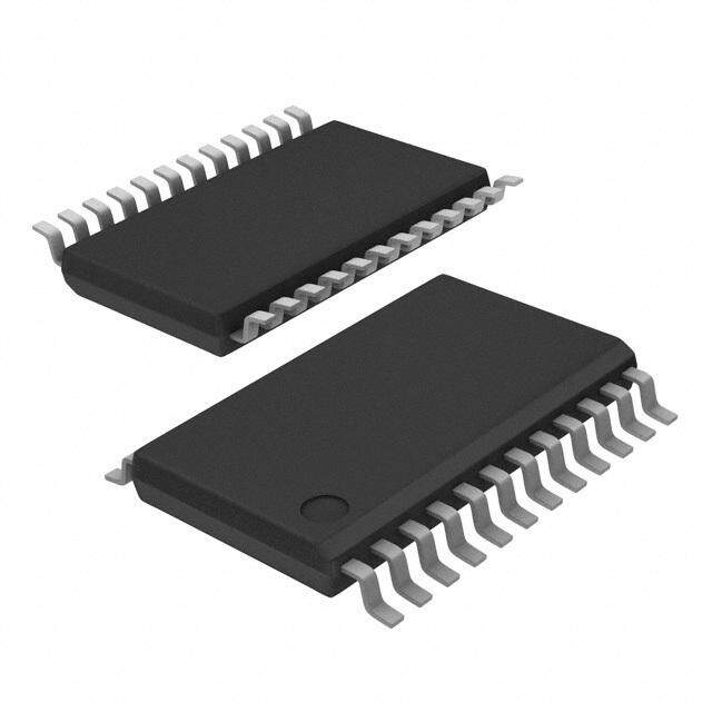
ICGOO电子元器件商城为您提供74LCX162244MTDX由Fairchild Semiconductor设计生产,在icgoo商城现货销售,并且可以通过原厂、代理商等渠道进行代购。 74LCX162244MTDX价格参考¥5.27-¥5.32。Fairchild Semiconductor74LCX162244MTDX封装/规格:逻辑 - 缓冲器,驱动器,接收器,收发器, Buffer, Non-Inverting 4 Element 4 Bit per Element 3-State Output 48-TSSOP。您可以下载74LCX162244MTDX参考资料、Datasheet数据手册功能说明书,资料中有74LCX162244MTDX 详细功能的应用电路图电压和使用方法及教程。
74LCX162244MTDX是安森美(ON Semiconductor)生产的一款16位总线缓冲器/驱动器,属于低电压CMOS逻辑系列,具有5V输入耐压能力。该器件主要用于数字系统中实现信号的双向缓冲与驱动,在高噪声或长距离传输环境中确保信号完整性。

典型应用场景包括:
1. 数据总线隔离与驱动:在微处理器、微控制器或FPGA系统中,用于隔离和增强数据总线驱动能力,减少负载对核心电路的影响。
2. 存储器接口扩展:连接存储器模块与主控芯片时,提升信号驱动强度,支持多设备共享总线。
3. 工业控制设备:广泛应用于PLC、工控机等工业自动化系统中,用于电平转换和信号调理。
4. 通信系统:在背板通信或多板互联系统中,作为信号中继器,提高抗干扰能力。
5. 消费类电子产品:如打印机、扫描仪等外设中,用于接口电平匹配和信号缓冲。

该器件采用TSSOP-48封装,支持宽温度范围,适用于紧凑型高密度PCB设计。其低功耗特性适合便携式设备,而5V容限输入可兼容TTL及5V CMOS电平,便于与旧有系统接口对接。整体上,74LCX162244MTDX是一款高性能、高可靠性的总线接口解决方案,适用于多种需要高速、稳定信号传输的数字系统环境。
| 参数 | 数值 |
| 产品目录 | 集成电路 (IC)半导体 |
| 描述 | IC BUFF DVR 16BIT LOW V 48TSSOP缓冲器和线路驱动器 16-Bit Buf/Line Drv |
| 产品分类 | |
| 品牌 | Fairchild Semiconductor |
| 产品手册 | |
| 产品图片 |
|
| rohs | 符合RoHS无铅 / 符合限制有害物质指令(RoHS)规范要求 |
| 产品系列 | 逻辑集成电路,缓冲器和线路驱动器,Fairchild Semiconductor 74LCX162244MTDX74LCX |
| 数据手册 | |
| 产品型号 | 74LCX162244MTDX |
| 产品种类 | 缓冲器和线路驱动器 |
| 传播延迟时间 | 6 ns at 2.7 V, 5.3 ns at 3.3 V |
| 低电平输出电流 | 12 mA |
| 供应商器件封装 | 48-TSSOP |
| 元件数 | 4 |
| 其它名称 | 74LCX162244MTDXDKR |
| 包装 | Digi-Reel® |
| 单位重量 | 421 mg |
| 商标 | Fairchild Semiconductor |
| 安装类型 | 表面贴装 |
| 安装风格 | SMD/SMT |
| 封装 | Reel |
| 封装/外壳 | 48-TFSOP(0.240",6.10mm 宽) |
| 封装/箱体 | TSSOP-48 |
| 工作温度 | -40°C ~ 85°C |
| 工厂包装数量 | 1000 |
| 最大工作温度 | + 85 C |
| 最小工作温度 | - 40 C |
| 极性 | Non-Inverting |
| 标准包装 | 1 |
| 每元件位数 | 4 |
| 每芯片的通道数量 | 16 |
| 电压-电源 | 2 V ~ 3.6 V |
| 电流-输出高,低 | 12mA,12mA |
| 电源电压-最大 | 3.6 V |
| 电源电压-最小 | 2 V |
| 系列 | 74LCX162244 |
| 输入线路数量 | 16 |
| 输出类型 | 3-State |
| 输出线路数量 | 16 |
| 逻辑类型 | 缓冲器/线路驱动器,非反相 |
| 逻辑系列 | LCX |
| 零件号别名 | 74LCX162244MTDX_NL |
| 高电平输出电流 | - 12 mA |


- 商务部:美国ITC正式对集成电路等产品启动337调查
- 曝三星4nm工艺存在良率问题 高通将骁龙8 Gen1或转产台积电
- 太阳诱电将投资9.5亿元在常州建新厂生产MLCC 预计2023年完工
- 英特尔发布欧洲新工厂建设计划 深化IDM 2.0 战略
- 台积电先进制程称霸业界 有大客户加持明年业绩稳了
- 达到5530亿美元!SIA预计今年全球半导体销售额将创下新高
- 英特尔拟将自动驾驶子公司Mobileye上市 估值或超500亿美元
- 三星加码芯片和SET,合并消费电子和移动部门,撤换高东真等 CEO
- 三星电子宣布重大人事变动 还合并消费电子和移动部门
- 海关总署:前11个月进口集成电路产品价值2.52万亿元 增长14.8%


PDF Datasheet 数据手册内容提取
Is Now Part of To learn more about ON Semiconductor, please visit our website at www.onsemi.com Please note: As part of the Fairchild Semiconductor integration, some of the Fairchild orderable part numbers will need to change in order to meet ON Semiconductor’s system requirements. Since the ON Semiconductor product management systems do not have the ability to manage part nomenclature that utilizes an underscore (_), the underscore (_) in the Fairchild part numbers will be changed to a dash (-). This document may contain device numbers with an underscore (_). Please check the ON Semiconductor website to verify the updated device numbers. The most current and up-to-date ordering information can be found at www.onsemi.com. Please email any questions regarding the system integration to Fairchild_questions@onsemi.com. ON Semiconductor and the ON Semiconductor logo are trademarks of Semiconductor Components Industries, LLC dba ON Semiconductor or its subsidiaries in the United States and/or other countries. ON Semiconductor owns the rights to a number of patents, trademarks, copyrights, trade secrets, and other intellectual property. A listing of ON Semiconductor’s product/patent coverage may be accessed at www.onsemi.com/site/pdf/Patent-Marking.pdf. ON Semiconductor reserves the right to make changes without further notice to any products herein. ON Semiconductor makes no warranty, representation or guarantee regarding the suitability of its products for any particular purpose, nor does ON Semiconductor assume any liability arising out of the application or use of any product or circuit, and specifically disclaims any and all liability, including without limitation special, consequential or incidental damages. Buyer is responsible for its products and applications using ON Semiconductor products, including compliance with all laws, regulations and safety requirements or standards, regardless of any support or applications information provided by ON Semiconductor. “Typical” parameters which may be provided in ON Semiconductor data sheets and/or specifications can and do vary in different applications and actual performance may vary over time. All operating parameters, including “Typicals” must be validated for each customer application by customer’s technical experts. ON Semiconductor does not convey any license under its patent rights nor the rights of others. ON Semiconductor products are not designed, intended, or authorized for use as a critical component in life support systems or any FDA Class 3 medical devices or medical devices with a same or similar classification in a foreign jurisdiction or any devices intended for implantation in the human body. Should Buyer purchase or use ON Semiconductor products for any such unintended or unauthorized application, Buyer shall indemnify and hold ON Semiconductor and its officers, employees, subsidiaries, affiliates, and distributors harmless against all claims, costs, damages, and expenses, and reasonable attorney fees arising out of, directly or indirectly, any claim of personal injury or death associated with such unintended or unauthorized use, even if such claim alleges that ON Semiconductor was negligent regarding the design or manufacture of the part. ON Semiconductor is an Equal Opportunity/Affirmative Action Employer. This literature is subject to all applicable copyright laws and is not for resale in any manner.
7 4 September 2000 L Revised May 2005 C X 1 6 2 74LCX162244 2 4 4 Low Voltage 16-Bit Buffer/Line Driver L with 26(cid:1) Series Resistors in Outputs ow V o General Description Features l t a The LCX162244 contains sixteen non-inverting buffers with (cid:1) 5V tolerant inputs and outputs g 3a-nSdT aAdTdEr eosust pdurtivse dr,e csliogcnke dd rtiov ebr,e oer mbpulso yoerdie natse da tmraenmsmority- (cid:1) 2.3V–3.6V VCC specifications provided e 1 (cid:1) Outputs include equivalent series resistance of 26: to 6 ter/receiver. The device is nibble controlled. Each nibble - make external termination resistors unnecessary and B has separate 3-STATE control inputs which can be shorted tTohgee tLhCeXr f1o6r2 f2u4ll 41 6is- bdite osipgenreadti ofonr. low voltage (2.5V or 3.3V) (cid:1) r5e.3d uncse t PoDve mrsahxo (oVt CaCn d u3n.0dVe)r,s h2o0o PtA ICC max it B u VCC applications with capability of interfacing to a 5V signal (cid:1) Power down high impedance inputs and outputs ff environment. (cid:1) r12 mA output drive (VCC 3.0V) er In addition, the outputs include equivalent 26: (nominal) (cid:1) Implements patented noise/EMI reduction circuitry /L series resistors to reduce overshoot and undershoot and (cid:1) Latch-up performance exceeds 500 mA in aTrhee d LeCsiXgn1e6d2 2to4 4s inisk /sfaoburriccea tuepd tow i1th2 manA aatd VvaCnCc e d3 .C0VM.OS (cid:1) ESD performance: e D tinegch CnMolOogSy ltoow a pcohiweevre dhiisgship saptieoend. operation while maintain- HMuamchainne b modoyd mel o!d 2el0 !0 V2000V riv e (cid:1) Also packaged in plastic Fine-Pitch Ball Grid Array r (FBGA) (Preliminary) w it h Ordering Code: 2 6 (cid:1) Order Number Package Number Package Description S 74LCX162244GX BGA54A 54-Ball Fine-Pitch Ball Grid Array (FBGA), JEDEC MO-205, 5.5mm Wide e r (Note 1) (Preliminary) [TAPE and REEL] ie 74LCX162244MEA MS48A 48-Lead Small Shrink Outline Package (SSOP), JEDEC MO-118, 0.300" Wide s (Note 2) R 74LCX162244MTD MTD48 48-Lead Thin Shrink Small Outline Package (TSSOP), JEDEC MO-153, 6.1mm Wide e s (Note 2) is Note 1: BGA package available in Tape and Reel only. to Note 2: Devices also available in Tape and Reel. Specify by appending the suffix letter “X” to the ordering code. r s Logic Symbol in O u t p u t s © 2005 Fairchild Semiconductor Corporation DS500471 www.fairchildsemi.com
4 4 Connection Diagrams Pin Descriptions 2 2 6 1 Pin Assignment for SSOP and TSSOP Pin Names Description X C OEn Output Enable Input (Active LOW) L 4 I0–I15 Inputs 7 O0–O15 Outputs NC No Connect FBGA Pin Assignments 1 2 3 4 5 6 A O0 NC OE1 OE2 NC I0 B O2 O1 NC NC I1 I2 C O4 O3 VCC VCC I3 I4 D O6 O5 GND GND I5 I6 E O8 O7 GND GND I7 I8 F O10 O9 GND GND I9 I10 G O12 O11 VCC VCC I11 I12 H O14 O13 NC NC I13 I14 J O15 NC OE4 OE3 NC I15 Truth Tables Inputs Outputs OE1 I0–I3 O0–O3 L L L Pin Assignment for FBGA L H H H X Z Inputs Outputs OE2 I4–I7 O4–O7 L L L L H H H X Z Inputs Outputs OE3 I8–I11 O8–O11 L L L (Top Thru View) L H H H X Z Inputs Outputs OE4 I12–I15 O12–O15 L L L L H H H X Z H HIGH Voltage Level L LOW Voltage Level X Immaterial Z High Impedance www.fairchildsemi.com 2
7 Functional Description 4 L The LCX162244 contains sixteen non-inverting buffers with can be shorted together to obtain full 16-bit operation. The C X 3-STATE standard outputs. The device is designed with 3-STATE outputs are controlled by an Output Enable (OEn) 1 26: series resistors in the outputs. This design reduces input for each nibble. When OEn is LOW, the outputs are in 6 line noise in applications such as memory address drivers, 2-state mode. When OEn is HIGH, the outputs are in the 22 clock drivers and bus transceiver/transmitters. The device high impedance mode, but this does not interfere with 4 is nibble (4 bits) controlled with each nibble functioning 4 entering new data into the inputs. identically, but independent of the other. The control pins Logic Diagram 3 www.fairchildsemi.com
4 4 Absolute Maximum Ratings 2 (Note 3) 2 6 Symbol Parameter Value Conditions Units 1 X VCC Supply Voltage (cid:16)0.5 to (cid:14)7.0 V C L VI DC Input Voltage (cid:16)0.5 to (cid:14)7.0 V 74 VO DC Output Voltage (cid:16)0.5 to (cid:14)7.0 Output in 3-STATE V (cid:16)0.5 to VCC (cid:14) 0.5 Output in HIGH or LOW State (Note 4) IIK DC Input Diode Current (cid:16)50 VI (cid:31) GND mA IOK DC Output Diode Current (cid:16)50 VO (cid:31) GND mA (cid:14)50 VO ! VCC IO DC Output Source/Sink Current r50 mA ICC DC Supply Current per Supply Pin r100 mA IGND DC Ground Current per Ground Pin r100 mA TSTG Storage Temperature (cid:16)65 to (cid:14)150 qC Recommended Operating Conditions (Note 5) Symbol Parameter Min Max Units VCC Supply Voltage Operating 2.0 3.6 V Data Retention 1.5 3.6 VI Input Voltage 0 5.5 V VO Output Voltage HIGH or LOW State 0 VCC V 3-STATE 0 5.5 IOH/IOL Output Current VCC 3.0V (cid:16) 3.6V r12 VCC 2.7V (cid:16) 3.0V r8 mA VCC 2.3V (cid:16) 2.7V r4 TA Free-Air Operating Temperature (cid:16)40 85 qC ’t/’V Input Edge Rate, VIN 0.8V–2.0V, VCC 3.0V 0 10 ns/V Note 3: The Absolute Maximum Ratings are those values beyond which the safety of the device cannot be guaranteed. The device should not be operated at these limits. The parametric values defined in the Electrical Characteristics tables are not guaranteed at the Absolute Maximum Ratings. The “Recom- mended Operating Conditions” table will define the conditions for actual device operation. Note 4: IO Absolute Maximum Rating must be observed. Note 5: Unused control inputs must be held HIGH or LOW. They may not float. DC Electrical Characteristics VCC TA (cid:16)40qC to (cid:14)85qC Symbol Parameter Conditions Units (V) Min Max VIH HIGH Level Input Voltage 2.3 (cid:16) 2.7 1.7 V 2.7 (cid:16) 3.6 2.0 VIL LOW Level Input Voltage 2.3 (cid:16) 2.7 0.7 V 2.7 (cid:16) 3.6 0.8 VOH HIGH Level Output Voltage IOH (cid:16)100 PA 2.3 (cid:16) 3.6 VCC (cid:16) 0.2 IOH (cid:16)4 mA 2.3 1.8 IOH (cid:16)4 mA 2.7 2.2 V IOH (cid:16)6 mA 3.0 2.4 IOH (cid:16)8 mA 2.7 2.0 IOH (cid:16)12 mA 3.0 2.0 VOL LOW Level Output Voltage IOL 100 PA 2.3 (cid:16) 3.6 0.2 IOL 4 mA 2.3 0.6 IOL 4 mA 2.7 0.4 V IOL 6 mA 3.0 0.55 IOL 8 mA 2.7 0.6 IOL 12 mA 3.0 0.8 II Input Leakage Current 0 d VI d 5.5 2.3 (cid:16) 3.6 r5.0 PA IOZ 3-STATE Output Leakage 0 d VO d 5.5V 2.3 (cid:16) 3.6 r5.0 PA VI VIH or VIL www.fairchildsemi.com 4
7 DC Electrical Characteristics 4 (Continued) L C X VCC TA (cid:16)40qC to (cid:14)85qC 1 Symbol Parameter Conditions Units 6 (V) Min Max 2 IOFF Power-Off Leakage Current VIN or VO 5.5V 0 10 PA 24 ICC Quiescent Supply Current VI VCC or GND 2.3 (cid:16) 3.6 20 PA 4 ’ICC Increase in ICC per Input VIH VCC (cid:16)0.6V 2.3 (cid:16) 3.6 500 PA Note 6: An external driver must source at least the specified current to switch from LOW-to-HIGH. Note 7: An external driver must sink at least the specified current to switch from HIGH-to-LOW. AC Electrical Characteristics TA (cid:16)40qC to (cid:14)85qC, RL 500 : VCC 3.3V r 0.3V VCC 2.7V VCC 2.5V r 0.2V Symbol Parameter Units CL 50 pF CL 50 pF CL 30 pF Min Max Min Max Min Max tPHL Propagation Delay 1.0 5.3 1.0 6.0 1.0 6.4 ns tPLH Data to Output 1.0 5.3 1.0 6.0 1.0 6.4 tPZL Output Enable Time 1.0 6.3 1.0 7.1 1.0 8.2 ns tPZH 1.0 6.3 1.0 7.1 1.0 8.2 tPLZ Output Disable Time 1.0 5.4 1.0 5.7 1.0 6.5 ns tPHZ 1.0 5.4 1.0 5.7 1.0 6.5 tOSHL Output to Output Skew (Note 8) 1.0 ns tOSLH 1.0 Note 8: Skew is defined as the absolute value of the difference between the actual propagation delay for any two separate outputs of the same device. The specification applies to any outputs switching in the same direction, either HIGH-to-LOW (tOSHL) or LOW-to-HIGH (tOSLH). Parameter guaranteed by design. Dynamic Switching Characteristics VCC TA 25qC Symbol Parameter Conditions Units (V) Typical VOLP Quiet Output Dynamic Peak VOL CL 50 pF, VIH 3.3V, VIL 0V 3.3 0.35 V CL 30 pF, VIH 2.5V, VIL 0V 2.5 0.25 VOLV Quiet Output Dynamic Valley VOL CL 50 pF, VIH 3.3V, VIL 0V 3.3 (cid:16)0.35 V CL 30 pF, VIH 2.5V, VIL 0V 2.5 (cid:16)0.25 Capacitance Symbol Parameter Conditions Typical Units CIN Input Capacitance VCC Open, VI 0V or VCC 7 pF COUT Output Capacitance VCC 3.3V, VI 0V or VCC 8 pF CPD Power Dissipation Capacitance VCC 3.3V, VI 0V or VCC, f 10 MHz 20 pF 5 www.fairchildsemi.com
4 4 AC LOADING and WAVEFORMS 2 Generic for LCX Family 2 6 1 X C L 4 7 FIGURE 1. AC Test Circuit (CL includes probe and jig capacitance) VI CL 6V for VCC 3.3V, 2.7V 50 pF VCC * 2 for VCC 2.5V 30 pF Waveform for Inverting and Non-Inverting Functions 3-STATE Output High Enable and Disable Times for Logic Propagation Delay. Pulse Width and trec Waveforms Setup Time, Hold Time and Recovery Time for Logic 3-STATE Output Low Enable and trise and tfall Disable Times for Logic FIGURE 2. Waveforms (Input Characteristics; f =1MHz, tr = tf = 3ns) VCC Symbol 3.3V r 0.3V 2.7V 2.5V r 0.2V Vmi 1.5V 1.5V VCC/2 Vmo 1.5V 1.5V VCC/2 Vx VOL (cid:14) 0.3V VOL (cid:14) 0.3V VOL (cid:14) 0.15V Vy VOH (cid:16) 0.3V VOH (cid:16) 0.3V VOH (cid:16) 0.15V www.fairchildsemi.com 6
7 Schematic Diagram 4 Generic for LCX Family L C X 1 6 2 2 4 4 7 www.fairchildsemi.com
4 4 Physical Dimensions 2 inches (millimeters) unless otherwise noted 2 6 1 X C L 4 7 54-Ball Fine-Pitch Ball Grid Array (FBGA), JEDEC MO-205, 5.5mm Wide Package Number BGA54A Preliminary www.fairchildsemi.com 8
7 Physical Dimensions 4 inches (millimeters) unless otherwise noted (Continued) L C X 1 6 2 2 4 4 48-Lead Small Shrink Outline Package (SSOP), JEDEC MO-118, 0.300" Wide Package Number MS48A 9 www.fairchildsemi.com
s ut Physical Dimensions inches (millimeters) unless otherwise noted (Continued) p t u O n i s r o t s si e R s e i r e S (cid:1) 6 2 h t i w r e v i r D e n i L / r e f f u B t i B - 6 1 e g a t l o V w o L 4 4 2 2 48-Lead Thin Shrink Small Outline Package (TSSOP), JEDEC MO-153, 6.1mm Wide 6 1 Package Number MTD48 X C L 4 7 Fairchild does not assume any responsibility for use of any circuitry described, no circuit patent licenses are implied and Fairchild reserves the right at any time without notice to change said circuitry and specifications. LIFE SUPPORT POLICY FAIRCHILD’S PRODUCTS ARE NOT AUTHORIZED FOR USE AS CRITICAL COMPONENTS IN LIFE SUPPORT DEVICES OR SYSTEMS WITHOUT THE EXPRESS WRITTEN APPROVAL OF THE PRESIDENT OF FAIRCHILD SEMICONDUCTOR CORPORATION. As used herein: 1. Life support devices or systems are devices or systems 2. A critical component in any component of a life support which, (a) are intended for surgical implant into the device or system whose failure to perform can be rea- body, or (b) support or sustain life, and (c) whose failure sonably expected to cause the failure of the life support to perform when properly used in accordance with device or system, or to affect its safety or effectiveness. instructions for use provided in the labeling, can be rea- sonably expected to result in a significant injury to the www.fairchildsemi.com user. www.fairchildsemi.com 10
ON Semiconductor and are trademarks of Semiconductor Components Industries, LLC dba ON Semiconductor or its subsidiaries in the United States and/or other countries. ON Semiconductor owns the rights to a number of patents, trademarks, copyrights, trade secrets, and other intellectual property. A listing of ON Semiconductor’s product/patent coverage may be accessed at www.onsemi.com/site/pdf/Patent−Marking.pdf. ON Semiconductor reserves the right to make changes without further notice to any products herein. ON Semiconductor makes no warranty, representation or guarantee regarding the suitability of its products for any particular purpose, nor does ON Semiconductor assume any liability arising out of the application or use of any product or circuit, and specifically disclaims any and all liability, including without limitation special, consequential or incidental damages. Buyer is responsible for its products and applications using ON Semiconductor products, including compliance with all laws, regulations and safety requirements or standards, regardless of any support or applications information provided by ON Semiconductor. “Typical” parameters which may be provided in ON Semiconductor data sheets and/or specifications can and do vary in different applications and actual performance may vary over time. All operating parameters, including “Typicals” must be validated for each customer application by customer’s technical experts. ON Semiconductor does not convey any license under its patent rights nor the rights of others. ON Semiconductor products are not designed, intended, or authorized for use as a critical component in life support systems or any FDA Class 3 medical devices or medical devices with a same or similar classification in a foreign jurisdiction or any devices intended for implantation in the human body. Should Buyer purchase or use ON Semiconductor products for any such unintended or unauthorized application, Buyer shall indemnify and hold ON Semiconductor and its officers, employees, subsidiaries, affiliates, and distributors harmless against all claims, costs, damages, and expenses, and reasonable attorney fees arising out of, directly or indirectly, any claim of personal injury or death associated with such unintended or unauthorized use, even if such claim alleges that ON Semiconductor was negligent regarding the design or manufacture of the part. ON Semiconductor is an Equal Opportunity/Affirmative Action Employer. This literature is subject to all applicable copyright laws and is not for resale in any manner. PUBLICATION ORDERING INFORMATION LITERATURE FULFILLMENT: N. American Technical Support: 800−282−9855 Toll Free ON Semiconductor Website: www.onsemi.com Literature Distribution Center for ON Semiconductor USA/Canada 19521 E. 32nd Pkwy, Aurora, Colorado 80011 USA Europe, Middle East and Africa Technical Support: Order Literature: http://www.onsemi.com/orderlit Phone: 303−675−2175 or 800−344−3860 Toll Free USA/Canada Phone: 421 33 790 2910 Fax: 303−675−2176 or 800−344−3867 Toll Free USA/Canada Japan Customer Focus Center For additional information, please contact your local Email: orderlit@onsemi.com Phone: 81−3−5817−1050 Sales Representative © Semiconductor Components Industries, LLC www.onsemi.com www.onsemi.com 1
Mouser Electronics Authorized Distributor Click to View Pricing, Inventory, Delivery & Lifecycle Information: O N Semiconductor: 74LCX162244MEA 74LCX162244MTD 74LCX162244MEAX 74LCX162244MTDX