ICGOO在线商城 > 集成电路(IC) > 逻辑 - 缓冲器,驱动器,接收器,收发器 > 74HCT7541N,112
 Datasheet下载
- 型号: 74HCT7541N,112
- 制造商: NXP Semiconductors
- 库位|库存: xxxx|xxxx
- 要求:
| 数量阶梯 | 香港交货 | 国内含税 |
| +xxxx | $xxxx | ¥xxxx |
查看当月历史价格
查看今年历史价格
74HCT7541N,112产品简介:
ICGOO电子元器件商城为您提供74HCT7541N,112由NXP Semiconductors设计生产,在icgoo商城现货销售,并且可以通过原厂、代理商等渠道进行代购。 74HCT7541N,112价格参考。NXP Semiconductors74HCT7541N,112封装/规格:逻辑 - 缓冲器,驱动器,接收器,收发器, Buffer, Non-Inverting 1 Element 8 Bit per Element 3-State Output 20-DIP。您可以下载74HCT7541N,112参考资料、Datasheet数据手册功能说明书,资料中有74HCT7541N,112 详细功能的应用电路图电压和使用方法及教程。
NXP USA Inc. 生产的 74HCT7541N 是一款逻辑缓冲器、驱动器和接收器,属于 74HCT 系列。以下是其主要应用场景:

 1. 信号缓冲与驱动
   - 功能:74HCT7541N 可用于增强数字信号的驱动能力,确保信号能够传输到更远的距离或驱动更多的负载。
   - 应用场景:在复杂的电路设计中,当需要将一个微弱的信号放大以驱动多个负载时,该芯片可以作为信号缓冲器使用。例如,在多路复用器或数据总线中,它可以帮助稳定信号并减少信号失真。

 2. 电平转换
   - 功能:由于 74HCT 系列兼容 TTL 和 CMOS 电平,74HCT7541N 可用于不同逻辑电平之间的转换。
   - 应用场景:在混合信号系统中,例如将低电压 MCU 的输出信号(如 3.3V)转换为高电压信号(如 5V),以驱动外部设备或接口。

 3. 数据传输与通信
   - 功能:该芯片支持高速数据传输,适用于需要快速切换状态的应用。
   - 应用场景:可用于串行通信接口(如 UART、SPI 或 I2C)中的信号调理,确保数据的完整性和可靠性。例如,在工业自动化或嵌入式系统中,它可以作为数据收发器的一部分。

 4. 多路输入/输出控制
   - 功能:74HCT7541N 提供多路输入和输出引脚,能够同时处理多个信号通道。
   - 应用场景:在需要控制多个 LED、继电器或其他外设的系统中,可以用作多路信号分配器或控制器。例如,在交通信号灯控制系统或家用自动化设备中。

 5. 时钟信号分发
   - 功能:该芯片可以用来分发时钟信号,确保所有相关模块同步工作。
   - 应用场景:在数字时钟、计时器或音频设备中,74HCT7541N 可以帮助将主时钟信号分配到不同的子模块,保持系统的同步性。

 6. 抗干扰与稳定性提升
   - 功能:通过缓冲和放大信号,减少噪声对信号的影响。
   - 应用场景:在嘈杂的电磁环境中(如工厂或汽车电子系统),该芯片可以提高信号的抗干扰能力,确保系统的稳定运行。

总之,74HCT7541N 在需要信号增强、电平转换、多路控制和数据传输的场景中具有广泛应用,尤其适合工业控制、通信设备、消费电子和汽车电子等领域。
| 参数 | 数值 |
| 产品目录 | 集成电路 (IC)半导体 |
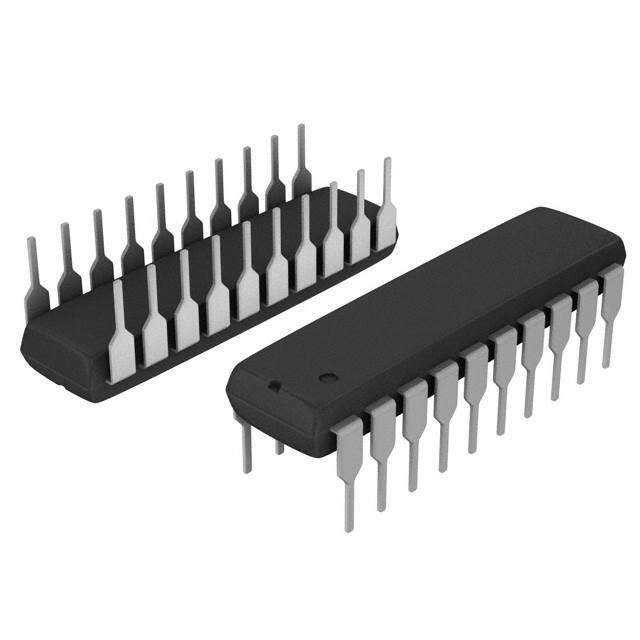
| 描述 | IC SCHMT TRIG BUFF/DVR 8B 20DIP缓冲器和线路驱动器 OCT SCHM TRIG |
| 产品分类 | |
| 品牌 | NXP Semiconductors |
| 产品手册 | |
| 产品图片 |
|
| rohs | 符合RoHS无铅 / 符合限制有害物质指令(RoHS)规范要求 |
| 产品系列 | 逻辑集成电路,缓冲器和线路驱动器,NXP Semiconductors 74HCT7541N,11274HCT |
| 数据手册 | |
| 产品型号 | 74HCT7541N,112 |
| PCN封装 | |
| PCN组件/产地 | |
| 产品培训模块 | http://www.digikey.cn/PTM/IndividualPTM.page?site=cn&lang=zhs&ptm=24983 |
| 产品种类 | Buffers, Line Drivers |
| 传播延迟时间 | 16 ns |
| 低电平输出电流 | 6 mA |
| 供应商器件封装 | 20-DIP |
| 元件数 | 1 |
| 其它名称 | 568-2908-5 |
| 包装 | 管件 |
| 商标 | NXP Semiconductors |
| 安装类型 | 通孔 |
| 安装风格 | Through Hole |
| 封装 | Tube |
| 封装/外壳 | 20-DIP(0.300",7.62mm) |
| 封装/箱体 | DIP-20 |
| 工作温度 | -40°C ~ 125°C |
| 工厂包装数量 | 18 |
| 最大工作温度 | + 125 C |
| 最小工作温度 | - 40 C |
| 极性 | Non-Inverting |
| 标准包装 | 18 |
| 每元件位数 | 8 |
| 每芯片的通道数量 | 8 |
| 电压-电源 | 4.5 V ~ 5.5 V |
| 电流-输出高,低 | 6mA,6mA |
| 电源电压-最大 | 5.5 V |
| 电源电压-最小 | 4.5 V |
| 输入线路数量 | 8 |
| 输出类型 | 3-State |
| 输出线路数量 | 8 |
| 逻辑类型 | 施密特触发器 - 缓冲器,驱动器 |
| 逻辑系列 | HCT |
| 零件号别名 | 74HCT7541N |
| 高电平输出电流 | - 6 mA |


- 商务部:美国ITC正式对集成电路等产品启动337调查
- 曝三星4nm工艺存在良率问题 高通将骁龙8 Gen1或转产台积电
- 太阳诱电将投资9.5亿元在常州建新厂生产MLCC 预计2023年完工
- 英特尔发布欧洲新工厂建设计划 深化IDM 2.0 战略
- 台积电先进制程称霸业界 有大客户加持明年业绩稳了
- 达到5530亿美元!SIA预计今年全球半导体销售额将创下新高
- 英特尔拟将自动驾驶子公司Mobileye上市 估值或超500亿美元
- 三星加码芯片和SET,合并消费电子和移动部门,撤换高东真等 CEO
- 三星电子宣布重大人事变动 还合并消费电子和移动部门
- 海关总署:前11个月进口集成电路产品价值2.52万亿元 增长14.8%


PDF Datasheet 数据手册内容提取
74HC7541; 74HCT7541 Octal Schmitt trigger buffer/line driver; 3-state Rev. 6 — 16 December 2013 Product data sheet 1. General description The 74HC7541; 74HCT7541 is an 8-bit buffer/line driver with Schmitt-trigger inputs and 3-state outputs. The device features two output enables (OE1 and OE2). A HIGH on OEn causes the outputs to assume a high-impedance OFF-state. Inputs include clamp diodes. This enables the use of current limiting resistors to interface inputs to voltages in excess of V . Schmitt trigger inputs transform slowly changing input signals into sharply defined CC jitter-free output signals. 2. Features and benefits Non-inverting outputs Low-power dissipation Input levels: For 74HC7541: CMOS level For 74HCT7541: TTL level Complies with JEDEC standard no. 7A ESD protection: HBM JESD22-A114F exceeds 2000V MM JESD22-A115-A exceeds 200V Multiple package options Specified from 40C to +85C and from 40C to +125C 3. Ordering information Table 1. Ordering info rmation Type number Package Temperature range Name Description Version 74HC7541N 40Cto+125C DIP20 plastic dual in-line package; 20leads (300mil) SOT146-1 74HCT7541N 74HC7541D 40 C to +125 C SO20 plastic small outline package; 20leads; SOT163-1 bodywidth7.5mm 74HCT7541D 74HC7541DB 40 C to +125 C SSOP20 plastic shrink small outline package; 20 leads; SOT339-1 bodywidth5.3mm 74HC7541PW 40Cto+125C TSSOP20 plastic thin shrink small outline package; 20 leads; SOT360-1 bodywidth4.4mm 74HCT7541PW
74HC7541; 74HCT7541 NXP Semiconductors Octal Schmitt trigger buffer/line driver; 3-state 4. Functional diagram A0 Y0 2 18 A1 Y1 3 17 A2 Y2 4 16 A3 Y3 5 15 1 & EN 19 A4 Y4 6 14 2 18 A5 Y5 3 17 7 13 4 16 A6 Y6 5 15 8 12 6 14 A7 Y7 7 13 9 11 8 12 OE1 9 11 1 19 OE2 aaa-000084 aaa-000085 Fig 1. Logic symbol Fig 2. IEC logic symbol 5. Pinning information 5.1 Pinning 74HC7541 74HC7541 74HCT7541 74HCT7541 OE1 1 20 VCC OE1 1 20 VCC A0 2 19 OE2 AO 2 19 OE2 A1 3 18 Y0 A1 3 18 Y0 A2 4 17 Y1 A2 4 17 Y1 A3 5 16 Y2 A3 5 16 Y2 A4 6 15 Y3 A4 6 15 Y3 A5 7 14 Y4 A5 7 14 Y4 A6 8 13 Y5 A6 8 13 Y5 A7 9 12 Y6 A7 9 12 Y6 GND 10 11 Y7 GND 10 11 Y7 aaa-000086 aaa-000087 Fig 3. Pin configuration DIP20, SO20 Fig 4. Pin configuration SSOP20, TSSOP20 74HC_HCT7541 All information provided in this document is subject to legal disclaimers. © NXP B.V. 2013. All rights reserved. Product data sheet Rev. 6 — 16 December 2013 2 of 17
74HC7541; 74HCT7541 NXP Semiconductors Octal Schmitt trigger buffer/line driver; 3-state 5.2 Pin description Table 2. Pin descripti on Symbol Pin Description OE1 1 output enable input (active LOW) A0 to A7 2, 3, 4, 5, 6, 7, 8, 9 data input GND 10 ground (0V) Y0 to Y7 18, 17, 16, 15, 14, 13, 12, 11 data output OE2 19 output enable input (active LOW) V 20 supply voltage CC 6. Functional description Table 3. Functional ta ble[1] Control Input Output OE1 OE2 An Yn L L L L L L H H X H X Z H X X Z [1] H = HIGH voltage level; L = LOW voltage level; X = don’t care; Z = high-impedance OFF-state. 7. Limiting values Table 4. Limiting valu es In accordance with the Absolute Maximum Rating System (IEC 60134). Voltages are referenced to GND (ground = 0 V). Symbol Parameter Conditions Min Max Unit V supply voltage 0.5 +7 V CC I input clamping current V < 0.5V or V >V +0.5 V [1] - 20 mA IK I I CC I output clamping current V <0.5V or V >V +0.5V [1] - 20 mA OK O O CC I output current 0.5V < V < V +0.5V - 35 mA O O CC I supply current - 70 mA CC I ground current 70 - mA GND T storage temperature 65 +150 C stg P total power dissipation [2] tot DIP20 - 750 mW SO20, SSOP20, TSSOP20 - 500 mW [1] The input and output voltage ratings may be exceeded if the input and output current ratings are observed. [2] For DIP20 packages: above 70 C the value of Ptot derates linearly with 12 mW/K. For SO20 packages: above 70 C the value of Ptot derates linearly with 8 mW/K. For SSOP20 and TSSOP20 packages: above 60 C the value of Ptot derates linearly with 5.5 mW/K. 74HC_HCT7541 All information provided in this document is subject to legal disclaimers. © NXP B.V. 2013. All rights reserved. Product data sheet Rev. 6 — 16 December 2013 3 of 17
74HC7541; 74HCT7541 NXP Semiconductors Octal Schmitt trigger buffer/line driver; 3-state 8. Recommended operating conditions Table 5. Recommend ed operating conditions Voltages are referenced to GND (ground = 0V) Symbol Parameter Conditions 74HC7541 74HCT7541 Unit Min Typ Max Min Typ Max V supply voltage 2.0 5.0 6.0 4.5 5.0 5.5 V CC V input voltage 0 - V 0 - V V I CC CC V output voltage 0 - V 0 - V V O CC CC T ambient temperature 40 +25 +125 40 +25 +125 C amb 9. Static characteristics Table 6. Static charac teristics At recommended operating conditions; voltages are referenced to GND (ground = 0 V). Symbol Parameter Conditions T = 25 C T = 40C T = 40C Unit amb amb amb to+85 C to+125 C Min Typ Max Min Max Min Max 74HC7541 V HIGH-level V = V or V OH I T+ T output voltage I = 20A; V = 2.0V 1.9 2.0 - 1.9 - 1.9 - V O CC I = 20A; V = 4.5V 4.4 4.5 - 4.4 - 4.4 - V O CC I = 20A; V = 6.0V 5.9 6.0 - 5.9 - 5.9 - V O CC I = 6.0mA; V = 4.5V 3.98 4.32 - 3.84 - 3.7 - V O CC I = 7.8mA; V = 6.0V 5.48 5.81 - 5.34 - 5.2 - V O CC V LOW-level V = V or V OL I T+ T output voltage I = 20A; V = 2.0V - 0 0.1 - 0.1 - 0.1 V O CC I = 20A; V = 4.5V - 0 0.1 - 0.1 - 0.1 V O CC I = 20A; V = 6.0V - 0 0.1 - 0.1 - 0.1 V O CC I = 6.0mA; V = 4.5V - 0.15 0.26 - 0.33 - 0.4 V O CC I = 7.8mA; V = 6.0V - 0.16 0.26 - 0.33 - 0.4 V O CC I input leakage V = V or GND; V =6.0V - - 0.1 - 1.0 - 1.0 A I I CC CC current I OFF-state per input pin; V =V or V ; - - 0.5 - 5.0 - 10 A OZ I T+ T output current V =V or GND; O CC otherinputs at V or GND; CC V =6.0V; I =0A CC O I supply current V = V or GND; I =0A; - - 8.0 - 80 - 160 A CC I CC O V =6.0V CC C input - 3.5 - - - - - pF I capacitance 74HCT7541 V HIGH-level V = V or V ; V = 4.5V OH I T+ T CC output voltage I = 20A 4.4 4.5 - 4.4 - 4.4 - V O I = 6.0mA 3.98 4.32 - 3.84 - 3.7 - V O 74HC_HCT7541 All information provided in this document is subject to legal disclaimers. © NXP B.V. 2013. All rights reserved. Product data sheet Rev. 6 — 16 December 2013 4 of 17
74HC7541; 74HCT7541 NXP Semiconductors Octal Schmitt trigger buffer/line driver; 3-state Table 6. Static characteristics …continued At recommended operating conditions; voltages are referenced to GND (ground = 0 V). Symbol Parameter Conditions T = 25 C T = 40C T = 40C Unit amb amb amb to+85 C to+125 C Min Typ Max Min Max Min Max V LOW-level V = V or V ; V = 4.5V OL I T+ T CC output voltage I = 20A; - 0 0.1 - 0.1 - 0.1 V O I = 6.0mA; - 0.15 0.26 - 0.33 - 0.4 V O I input leakage V = V or GND; V =5.5V - - 0.1 - 1.0 - 1.0 A I I CC CC current I OFF-state per input pin; V =V or V ; - - 0.5 - 5.0 - 10 A OZ I T+ T output current V =V or GND; O CC otherinputs at V or GND; CC V =5.5V; I =0A CC O I supply current V =V orGND; I = 0 A; - - 8.0 - 80 - 160 A CC I CC O V =5.5V CC I additional per input pin; I =0A; CC O supply current V =V 2.1V; I CC otherinputsat V orGND; CC V =4.5Vto5.5V CC An input - 20 72 - 90 - 98 A OEn input - 130 468 - 585 - 637 A C input - 3.5 - - - - - pF I capacitance 10. Dynamic characteristics Table 7. Dynamic cha racteristics GND=0V; C =50pF; for test circuit see Figure7. L Symbol Parameter Conditions T = 25 C T = 40 C to +125 C Unit amb amb Min Typ Max Max (85C) Max (125C) 74HC7541 t propagation delay An to Yn; see Figure5 [1] pd V = 2.0 V - 39 120 150 180 ns CC V = 4.5 V - 14 24 30 36 ns CC V = 5.0 V; C =15pF - 10 - - - ns CC L V = 6.0 V - 11 20 26 32 ns CC t enable time OEntoYn; see Figure6 [1] en V = 2.0 V - 44 160 200 240 ns CC V = 4.5 V - 16 32 40 48 ns CC V = 6.0 V - 13 27 34 41 ns CC t disable time OEntoYn; see Figure6 [1] dis V = 2.0 V - 58 160 200 240 ns CC V = 4.5 V - 21 32 40 48 ns CC V = 6.0 V - 17 27 34 41 ns CC 74HC_HCT7541 All information provided in this document is subject to legal disclaimers. © NXP B.V. 2013. All rights reserved. Product data sheet Rev. 6 — 16 December 2013 5 of 17
74HC7541; 74HCT7541 NXP Semiconductors Octal Schmitt trigger buffer/line driver; 3-state Table 7. Dynamic characteristics GND=0V; C =50pF; for test circuit see Figure7. L Symbol Parameter Conditions T = 25 C T = 40 C to +125 C Unit amb amb Min Typ Max Max (85C) Max (125C) t transition time seeFigure5 [2] t V = 2.0 V - 14 60 75 90 ns CC V = 4.5 V - 5 12 15 18 ns CC V = 6.0 V - 4 10 13 15 ns CC C power dissipation per package; [3] - 30 - - - pF PD capacitance V =GNDtoV I CC 74HCT7541 t propagation delay An to Yn; see Figure5 [1] pd V = 4.5 V - 19 32 40 48 ns CC V = 5.0 V; C =15pF - 16 - - - ns CC L t enable time OEntoYn; see Figure6 [1] en V = 4.5 V - 18 32 40 48 ns CC t disable time OEntoYn; see Figure6 [1] dis V = 4.5 V - 20 32 40 48 ns CC t transition time V = 4.5 V; seeFigure5 [2] - 5 12 15 18 ns t CC C power dissipation per package; [3] - 32 - - - pF PD capacitance V =GNDtoV 1.5V I CC [1] t is the same as t and t . pd PLH PHL ten is the same as tPZL and tPZH. tdis is the same as tPLZ and tPHZ. [2] t is the same as t and t . t THL TLH [3] CPD is used to determine the dynamic power dissipation (PD in W): PD=CPDVCC2fiN+ (CLVCC2fo) where: fi =input frequency in MHz; fo=output frequency in MHz; CL=output load capacitance in pF; VCC=supply voltage in V; N=number of inputs switching; (CLVCC2fo)=sum of outputs. 74HC_HCT7541 All information provided in this document is subject to legal disclaimers. © NXP B.V. 2013. All rights reserved. Product data sheet Rev. 6 — 16 December 2013 6 of 17
74HC7541; 74HCT7541 NXP Semiconductors Octal Schmitt trigger buffer/line driver; 3-state 11. Waveforms Vl An input VM VM GND tPHL tPLH VOH 90 % Yn output VM VM 10 % VOL tTHL tTLH aaa-000088 Measurement points are given in Table8. VOL and VOH are typical voltage output levels that occur with the output load. Fig 5. Input to output propagation delays VI OEn input VM GND tPLZ tPZL VCC Yn output LOW-to-OFF VM OFF-to-LOW VOL VX tPHZ tPZH Yn output VOH VY HIGH-to-OFF VM OFF-to-HIGH GND outputs outputs outputs enabled disabled enabled aaa-000089 Measurement points are given in Table8. V and V are typical voltage output levels that occur with the output load. OL OH Fig 6. 3-state enable and disable times Table 8. Measuremen t points Type Input Output V V V V M M X Y 74HC7541 0.5V 0.5V 0.1V 0.9V CC CC CC CC 74HCT7541 1.3V 1.3V 0.1V 0.9V CC CC 74HC_HCT7541 All information provided in this document is subject to legal disclaimers. © NXP B.V. 2013. All rights reserved. Product data sheet Rev. 6 — 16 December 2013 7 of 17
74HC7541; 74HCT7541 NXP Semiconductors Octal Schmitt trigger buffer/line driver; 3-state tW VI 90 % negative pulse VM VM 10 % 0 V tf tr tr tf VI 90 % positive pulse VM VM 10 % 0 V tW VCC VCC VI VO RL S1 G DUT open RT CL 001aad983 Test data is given in Table9. Definitions test circuit: RT = Termination resistance should be equal to output impedance Zo of the pulse generator C = Load capacitance including jig and probe capacitance L RL = Load resistance S1 = Test selection switch Fig 7. Test circuit for measuring switching times Table 9. Test data Type Input Load S1 position V t, t C R t , t t , t t , t I r f L L PHL PLH PZH PHZ PZL PLZ 74HC7541 V 6ns 15pF, 50 pF 1k open GND V CC CC 74HCT7541 3V 6ns 15pF, 50 pF 1k open GND V CC 74HC_HCT7541 All information provided in this document is subject to legal disclaimers. © NXP B.V. 2013. All rights reserved. Product data sheet Rev. 6 — 16 December 2013 8 of 17
74HC7541; 74HCT7541 NXP Semiconductors Octal Schmitt trigger buffer/line driver; 3-state 12. Transfer characteristics Table 10. Transfer cha racteristics At recommended operating conditions; voltages are referenced to GND (ground = 0 V); see Figure8 and Figure9. Symbol Parameter Conditions T = 25 C T = 40C T = 40C Unit amb amb amb to+85 C to+125 C Min Typ Max Min Max Min Max 74HC7541 V positive-going V = 2.0 V - - 1.5 - 1.5 - 1.5 V T+ CC threshold V = 4.5 V - - 3.15 - 3.15 - 3.15 V CC voltage V = 6.0 V - - 4.2 - 4.2 - 4.2 V CC V negative-going V = 2.0 V 0.3 - - 0.3 - 0.3 - V T CC threshold V = 4.5 V 1.35 - - 1.35 - 1.35 - V CC voltage V = 6.0 V 1.8 - - 1.8 - 1.8 - V CC V hysteresis V = 2.0 V 0.1 0.20 - 0.1 - 0.1 - V H CC voltage V = 4.5 V 0.25 0.40 - 0.25 - 0.25 - V CC V = 6.0 V 0.3 0.5 - 0.3 - 0.3 - V CC 74HCT7541 V positive-going V = 4.5 V - - 2.0 - 2.0 - 2.0 V T+ CC threshold V = 5.5 V - - 2.1 - 2.1 - 2.1 V CC voltage V negative-going V = 4.5 V 0.7 - - 0.64 - 0.6 - V T CC threshold V = 5.5 V 0.8 - - 0.74 - 0.7 - V CC voltage V hysteresis V = 4.5 V 0.17 0.23 - - - - - V H CC voltage V = 5.5 V 0.17 0.23 - - - - - V CC 13. Transfer characteristics waveforms VO VT+ VI VH VT− VO VH VI VT− VT+ mnb154 mnb155 Fig 8. Transfer characteristics Fig 9. Transfer characteristics definitions 74HC_HCT7541 All information provided in this document is subject to legal disclaimers. © NXP B.V. 2013. All rights reserved. Product data sheet Rev. 6 — 16 December 2013 9 of 17
74HC7541; 74HCT7541 NXP Semiconductors Octal Schmitt trigger buffer/line driver; 3-state 14. Package outline DIP20: plastic dual in-line package; 20 leads (300 mil) SOT146-1 D ME e n a pl g n eati A2 A s L A1 c Z e w M b1 (e ) 1 b 20 11 MH pin 1 index E 1 10 0 5 10 mm scale DIMENSIONS (inch dimensions are derived from the original mm dimensions) UNIT mAax. mAi n1 . mAa 2x . b b1 c D(1) E(1) e e1 L ME MH w mZax(1.) 1.73 0.53 0.36 26.92 6.40 3.60 8.25 10.0 mm 4.2 0.51 3.2 2.54 7.62 0.254 2 1.30 0.38 0.23 26.54 6.22 3.05 7.80 8.3 0.068 0.021 0.014 1.060 0.25 0.14 0.32 0.39 inches 0.17 0.02 0.13 0.1 0.3 0.01 0.078 0.051 0.015 0.009 1.045 0.24 0.12 0.31 0.33 Note 1. Plastic or metal protrusions of 0.25 mm (0.01 inch) maximum per side are not included. OUTLINE REFERENCES EUROPEAN ISSUE DATE VERSION IEC JEDEC JEITA PROJECTION 99-12-27 SOT146-1 MS-001 SC-603 03-02-13 Fig 10. Package outline SOT146-1 (DIP20) 74HC_HCT7541 All information provided in this document is subject to legal disclaimers. © NXP B.V. 2013. All rights reserved. Product data sheet Rev. 6 — 16 December 2013 10 of 17
74HC7541; 74HCT7541 NXP Semiconductors Octal Schmitt trigger buffer/line driver; 3-state SO20: plastic small outline package; 20 leads; body width 7.5 mm SOT163-1 D E A X c y HE v M A Z 20 11 Q A2 A A1 (A 3 ) pin 1 index θ Lp L 1 10 detail X e w M bp 0 5 10 mm scale DIMENSIONS (inch dimensions are derived from the original mm dimensions) UNIT mAax. A1 A2 A3 bp c D(1) E(1) e HE L Lp Q v w y Z(1) θ 0.3 2.45 0.49 0.32 13.0 7.6 10.65 1.1 1.1 0.9 mm 2.65 0.25 1.27 1.4 0.25 0.25 0.1 0.1 2.25 0.36 0.23 12.6 7.4 10.00 0.4 1.0 0.4 8o 0.012 0.096 0.019 0.013 0.51 0.30 0.419 0.043 0.043 0.035 0o inches 0.1 0.01 0.05 0.055 0.01 0.01 0.004 0.004 0.089 0.014 0.009 0.49 0.29 0.394 0.016 0.039 0.016 Note 1. Plastic or metal protrusions of 0.15 mm (0.006 inch) maximum per side are not included. OUTLINE REFERENCES EUROPEAN ISSUE DATE VERSION IEC JEDEC JEITA PROJECTION 99-12-27 SOT163-1 075E04 MS-013 03-02-19 Fig 11. Package outline SOT163-1 (SO20) 74HC_HCT7541 All information provided in this document is subject to legal disclaimers. © NXP B.V. 2013. All rights reserved. Product data sheet Rev. 6 — 16 December 2013 11 of 17
74HC7541; 74HCT7541 NXP Semiconductors Octal Schmitt trigger buffer/line driver; 3-state SSOP20: plastic shrink small outline package; 20 leads; body width 5.3 mm SOT339-1 D E A X c y HE v M A Z 20 11 Q A2 A A1 (A 3 ) pin 1 index θ Lp L 1 10 detail X w M e bp 0 2.5 5 mm scale DIMENSIONS (mm are the original dimensions) UNIT mAax. A1 A2 A3 bp c D(1) E(1) e HE L Lp Q v w y Z(1) θ mm 2 00..2015 11..8605 0.25 00..3285 00..2009 77..40 55..42 0.65 77..96 1.25 10..0633 00..97 0.2 0.13 0.1 00..95 80oo Note 1. Plastic or metal protrusions of 0.2 mm maximum per side are not included. OUTLINE REFERENCES EUROPEAN ISSUE DATE VERSION IEC JEDEC JEITA PROJECTION 99-12-27 SOT339-1 MO-150 03-02-19 Fig 12. Package outline SOT339-1 (SSOP20) 74HC_HCT7541 All information provided in this document is subject to legal disclaimers. © NXP B.V. 2013. All rights reserved. Product data sheet Rev. 6 — 16 December 2013 12 of 17
74HC7541; 74HCT7541 NXP Semiconductors Octal Schmitt trigger buffer/line driver; 3-state TSSOP20: plastic thin shrink small outline package; 20 leads; body width 4.4 mm SOT360-1 D E A X c y HE v M A Z 20 11 Q A2 (A 3 ) A pin 1 index A1 θ Lp L 1 10 detail X w M e bp 0 2.5 5 mm scale DIMENSIONS (mm are the original dimensions) UNIT mAax. A1 A2 A3 bp c D(1) E(2) e HE L Lp Q v w y Z(1) θ mm 1.1 00..1055 00..9850 0.25 00..3109 00..21 66..64 44..53 0.65 66..62 1 00..7550 00..43 0.2 0.13 0.1 00..52 80oo Notes 1. Plastic or metal protrusions of 0.15 mm maximum per side are not included. 2. Plastic interlead protrusions of 0.25 mm maximum per side are not included. OUTLINE REFERENCES EUROPEAN ISSUE DATE VERSION IEC JEDEC JEITA PROJECTION 99-12-27 SOT360-1 MO-153 03-02-19 Fig 13. Package outline SOT360-1 (TSSOP20) 74HC_HCT7541 All information provided in this document is subject to legal disclaimers. © NXP B.V. 2013. All rights reserved. Product data sheet Rev. 6 — 16 December 2013 13 of 17
74HC7541; 74HCT7541 NXP Semiconductors Octal Schmitt trigger buffer/line driver; 3-state 15. Abbreviations Table 11. Abbreviation s Acronym Description CMOS Complementary Metal-Oxide Semiconductor DUT Device Under Test ESD ElectroStatic Discharge HBM Human Body Model LSTTL Low-power Schottky Transistor-Transistor Logic MM Machine Model 16. Revision history T able 12. Revision history Document ID Release date Data sheet status Change notice Supersedes 74HC_HCT7541 v.6 20131216 Product data sheet - 74HC_HCT7541 v.5 Modifications: • New general description (errata). 74HC_HCT7541 v.5 20121231 Product data sheet - 74HC_HCT7541 v.4 Modifications: • I added to static characteristics table. OZ 74HC_HCT7541 v.4 20111219 Product data sheet - 74HC_HCT7541 v.3 Modifications: • Legal pages updated. 74HC_HCT7541 v.3 20110725 Product data sheet - 74HC_HCT7541_CNV v.2 74HC_HCT7541_CNV v.2 19970917 Product specification - - 74HC_HCT7541 All information provided in this document is subject to legal disclaimers. © NXP B.V. 2013. All rights reserved. Product data sheet Rev. 6 — 16 December 2013 14 of 17
74HC7541; 74HCT7541 NXP Semiconductors Octal Schmitt trigger buffer/line driver; 3-state 17. Legal information 17.1 Data sheet status Document status[1][2] Product status[3] Definition Objective [short] data sheet Development This document contains data from the objective specification for product development. Preliminary [short] data sheet Qualification This document contains data from the preliminary specification. Product [short] data sheet Production This document contains the product specification. [1] Please consult the most recently issued document before initiating or completing a design. [2] The term ‘short data sheet’ is explained in section “Definitions”. [3] The product status of device(s) described in this document may have changed since this document was published and may differ in case of multiple devices. The latest product status information is available on the Internet at URLhttp://www.nxp.com. 17.2 Definitions Suitability for use — NXP Semiconductors products are not designed, authorized or warranted to be suitable for use in life support, life-critical or safety-critical systems or equipment, nor in applications where failure or Draft — The document is a draft version only. The content is still under malfunction of an NXP Semiconductors product can reasonably be expected internal review and subject to formal approval, which may result in to result in personal injury, death or severe property or environmental modifications or additions. NXP Semiconductors does not give any damage. NXP Semiconductors and its suppliers accept no liability for representations or warranties as to the accuracy or completeness of inclusion and/or use of NXP Semiconductors products in such equipment or information included herein and shall have no liability for the consequences of applications and therefore such inclusion and/or use is at the customer’s own use of such information. risk. Short data sheet — A short data sheet is an extract from a full data sheet Applications — Applications that are described herein for any of these with the same product type number(s) and title. A short data sheet is intended products are for illustrative purposes only. NXP Semiconductors makes no for quick reference only and should not be relied upon to contain detailed and representation or warranty that such applications will be suitable for the full information. For detailed and full information see the relevant full data specified use without further testing or modification. sheet, which is available on request via the local NXP Semiconductors sales office. In case of any inconsistency or conflict with the short data sheet, the Customers are responsible for the design and operation of their applications full data sheet shall prevail. and products using NXP Semiconductors products, and NXP Semiconductors accepts no liability for any assistance with applications or customer product Product specification — The information and data provided in a Product design. It is customer’s sole responsibility to determine whether the NXP data sheet shall define the specification of the product as agreed between Semiconductors product is suitable and fit for the customer’s applications and NXP Semiconductors and its customer, unless NXP Semiconductors and products planned, as well as for the planned application and use of customer have explicitly agreed otherwise in writing. In no event however, customer’s third party customer(s). Customers should provide appropriate shall an agreement be valid in which the NXP Semiconductors product is design and operating safeguards to minimize the risks associated with their deemed to offer functions and qualities beyond those described in the applications and products. Product data sheet. NXP Semiconductors does not accept any liability related to any default, damage, costs or problem which is based on any weakness or default in the 17.3 Disclaimers customer’s applications or products, or the application or use by customer’s third party customer(s). Customer is responsible for doing all necessary testing for the customer’s applications and products using NXP Limited warranty and liability — Information in this document is believed to Semiconductors products in order to avoid a default of the applications and be accurate and reliable. However, NXP Semiconductors does not give any the products or of the application or use by customer’s third party representations or warranties, expressed or implied, as to the accuracy or customer(s). NXP does not accept any liability in this respect. completeness of such information and shall have no liability for the consequences of use of such information. NXP Semiconductors takes no Limiting values — Stress above one or more limiting values (as defined in responsibility for the content in this document if provided by an information the Absolute Maximum Ratings System of IEC60134) will cause permanent source outside of NXP Semiconductors. damage to the device. Limiting values are stress ratings only and (proper) operation of the device at these or any other conditions above those given in In no event shall NXP Semiconductors be liable for any indirect, incidental, the Recommended operating conditions section (if present) or the punitive, special or consequential damages (including - without limitation - lost Characteristics sections of this document is not warranted. Constant or profits, lost savings, business interruption, costs related to the removal or repeated exposure to limiting values will permanently and irreversibly affect replacement of any products or rework charges) whether or not such the quality and reliability of the device. damages are based on tort (including negligence), warranty, breach of contract or any other legal theory. Terms and conditions of commercial sale — NXP Semiconductors products are sold subject to the general terms and conditions of commercial Notwithstanding any damages that customer might incur for any reason whatsoever, NXP Semiconductors’ aggregate and cumulative liability towards sale, as published at http://www.nxp.com/profile/terms, unless otherwise customer for the products described herein shall be limited in accordance agreed in a valid written individual agreement. In case an individual with the Terms and conditions of commercial sale of NXP Semiconductors. agreement is concluded only the terms and conditions of the respective agreement shall apply. NXP Semiconductors hereby expressly objects to Right to make changes — NXP Semiconductors reserves the right to make applying the customer’s general terms and conditions with regard to the changes to information published in this document, including without purchase of NXP Semiconductors products by customer. limitation specifications and product descriptions, at any time and without notice. This document supersedes and replaces all information supplied prior No offer to sell or license — Nothing in this document may be interpreted or to the publication hereof. construed as an offer to sell products that is open for acceptance or the grant, conveyance or implication of any license under any copyrights, patents or other industrial or intellectual property rights. 74HC_HCT7541 All information provided in this document is subject to legal disclaimers. © NXP B.V. 2013. All rights reserved. Product data sheet Rev. 6 — 16 December 2013 15 of 17
74HC7541; 74HCT7541 NXP Semiconductors Octal Schmitt trigger buffer/line driver; 3-state Export control — This document as well as the item(s) described herein product for such automotive applications, use and specifications, and (b) may be subject to export control regulations. Export might require a prior whenever customer uses the product for automotive applications beyond authorization from competent authorities. NXP Semiconductors’ specifications such use shall be solely at customer’s own risk, and (c) customer fully indemnifies NXP Semiconductors for any Non-automotive qualified products — Unless this data sheet expressly liability, damages or failed product claims resulting from customer design and states that this specific NXP Semiconductors product is automotive qualified, use of the product for automotive applications beyond NXP Semiconductors’ the product is not suitable for automotive use. It is neither qualified nor tested standard warranty and NXP Semiconductors’ product specifications. in accordance with automotive testing or application requirements. NXP Semiconductors accepts no liability for inclusion and/or use of non-automotive qualified products in automotive equipment or applications. 17.4 Trademarks In the event that customer uses the product for design-in and use in automotive applications to automotive specifications and standards, customer Notice: All referenced brands, product names, service names and trademarks (a) shall use the product without NXP Semiconductors’ warranty of the are the property of their respective owners. 18. Contact information For more information, please visit: http://www.nxp.com For sales office addresses, please send an email to: salesaddresses@nxp.com 74HC_HCT7541 All information provided in this document is subject to legal disclaimers. © NXP B.V. 2013. All rights reserved. Product data sheet Rev. 6 — 16 December 2013 16 of 17
74HC7541; 74HCT7541 NXP Semiconductors Octal Schmitt trigger buffer/line driver; 3-state 19. Contents 1 General description. . . . . . . . . . . . . . . . . . . . . . 1 2 Features and benefits . . . . . . . . . . . . . . . . . . . . 1 3 Ordering information. . . . . . . . . . . . . . . . . . . . . 1 4 Functional diagram . . . . . . . . . . . . . . . . . . . . . . 2 5 Pinning information. . . . . . . . . . . . . . . . . . . . . . 2 5.1 Pinning . . . . . . . . . . . . . . . . . . . . . . . . . . . . . . . 2 5.2 Pin description . . . . . . . . . . . . . . . . . . . . . . . . . 3 6 Functional description . . . . . . . . . . . . . . . . . . . 3 7 Limiting values. . . . . . . . . . . . . . . . . . . . . . . . . . 3 8 Recommended operating conditions. . . . . . . . 4 9 Static characteristics. . . . . . . . . . . . . . . . . . . . . 4 10 Dynamic characteristics. . . . . . . . . . . . . . . . . . 5 11 Waveforms . . . . . . . . . . . . . . . . . . . . . . . . . . . . . 7 12 Transfer characteristics . . . . . . . . . . . . . . . . . . 9 13 Transfer characteristics waveforms. . . . . . . . . 9 14 Package outline. . . . . . . . . . . . . . . . . . . . . . . . 10 15 Abbreviations. . . . . . . . . . . . . . . . . . . . . . . . . . 14 16 Revision history. . . . . . . . . . . . . . . . . . . . . . . . 14 17 Legal information. . . . . . . . . . . . . . . . . . . . . . . 15 17.1 Data sheet status . . . . . . . . . . . . . . . . . . . . . . 15 17.2 Definitions. . . . . . . . . . . . . . . . . . . . . . . . . . . . 15 17.3 Disclaimers. . . . . . . . . . . . . . . . . . . . . . . . . . . 15 17.4 Trademarks. . . . . . . . . . . . . . . . . . . . . . . . . . . 16 18 Contact information. . . . . . . . . . . . . . . . . . . . . 16 19 Contents. . . . . . . . . . . . . . . . . . . . . . . . . . . . . . 17 Please be aware that important notices concerning this document and the product(s) described herein, have been included in section ‘Legal information’. © NXP B.V. 2013. All rights reserved. For more information, please visit: http://www.nxp.com For sales office addresses, please send an email to: salesaddresses@nxp.com Date of release: 16 December 2013 Document identifier: 74HC_HCT7541