 Datasheet下载
- 型号: 74HCT374PW,118
- 制造商: NXP Semiconductors
- 库位|库存: xxxx|xxxx
- 要求:
| 数量阶梯 | 香港交货 | 国内含税 |
| +xxxx | $xxxx | ¥xxxx |
查看当月历史价格
查看今年历史价格
74HCT374PW,118产品简介:
ICGOO电子元器件商城为您提供74HCT374PW,118由NXP Semiconductors设计生产,在icgoo商城现货销售,并且可以通过原厂、代理商等渠道进行代购。 74HCT374PW,118价格参考。NXP Semiconductors74HCT374PW,118封装/规格:逻辑 - 触发器, 。您可以下载74HCT374PW,118参考资料、Datasheet数据手册功能说明书,资料中有74HCT374PW,118 详细功能的应用电路图电压和使用方法及教程。
Nexperia USA Inc. 生产的74HCT374PW,118是一款逻辑触发器集成电路,具体为D型透明锁存器(D-type transparent latch)。该器件属于74系列中的高速CMOS (HCT) 器件,广泛应用于各种数字电路设计中。以下是其主要应用场景:

 1. 数据缓冲与存储
74HCT374PW,118可以用于数据缓冲和临时存储。它具有8个独立的D型锁存器,每个锁存器都有一个数据输入(D)和一个输出(Q),能够在时钟信号的控制下将输入数据锁存并保持在输出端。这使得它非常适合用于数据总线缓冲、寄存器文件以及需要临时存储数据的应用场景。

 2. 接口扩展
在微处理器或微控制器系统中,74HCT374PW,118可以用作I/O接口扩展。通过将其连接到系统的地址总线和数据总线,可以增加系统的I/O端口数量。例如,在工业控制系统中,它可以用于扩展GPIO端口,以控制更多的外部设备或传感器。

 3. 同步控制
该器件的锁存功能使其适用于同步控制应用。通过与时钟信号同步,可以确保多个数据通道在同一时刻被更新,从而实现精确的时间控制。例如,在通信系统中,它可以用于同步传输数据,确保接收端和发送端的数据一致。

 4. 状态机设计
74HCT374PW,118还可以用于构建有限状态机(FSM)。通过组合多个锁存器和逻辑门,可以设计出复杂的控制逻辑,用于自动化系统、定时器或其他需要多状态切换的应用。

 5. 数字信号处理
在数字信号处理领域,74HCT374PW,118可以用于信号采样和暂存。例如,在音频处理或图像处理中,它可以用于暂时存储采样数据,以便后续处理。

 总结
74HCT374PW,118是一款多功能的D型透明锁存器,适用于数据缓冲、接口扩展、同步控制、状态机设计和数字信号处理等多种应用场景。其高速性能和低功耗特性使其成为许多数字电路设计中的理想选择。
| 参数 | 数值 |
| 产品目录 | 集成电路 (IC)半导体 |
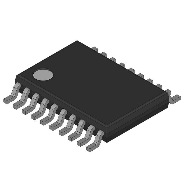
| 描述 | IC D-TYPE POS TRG SNGL 20TSSOP触发器 OCTAL D 3-STATE |
| 产品分类 | |
| 品牌 | NXP Semiconductors |
| 产品手册 | |
| 产品图片 |
|
| rohs | 符合RoHS无铅 / 符合限制有害物质指令(RoHS)规范要求 |
| 产品系列 | 逻辑集成电路,触发器,NXP Semiconductors 74HCT374PW,11874HCT |
| 数据手册 | |
| 产品型号 | 74HCT374PW,118 |
| PCN封装 | |
| PCN组件/产地 | |
| 不同V、最大CL时的最大传播延迟 | 32ns @ 4.5V,50pF |
| 产品培训模块 | http://www.digikey.cn/PTM/IndividualPTM.page?site=cn&lang=zhs&ptm=24983 |
| 产品种类 | 触发器 |
| 传播延迟时间 | 13 ns |
| 低电平输出电流 | 6 mA |
| 元件数 | 1 |
| 其它名称 | 568-7655-6 |
| 功能 | 标准 |
| 包装 | Digi-Reel® |
| 商标 | NXP Semiconductors |
| 安装类型 | 表面贴装 |
| 安装风格 | SMD/SMT |
| 封装 | Reel |
| 封装/外壳 | 20-TSSOP(0.173",4.40mm 宽) |
| 封装/箱体 | SOT-360 |
| 工作温度 | -40°C ~ 125°C (TA) |
| 工厂包装数量 | 2500 |
| 最大工作温度 | + 125 C |
| 最小工作温度 | - 40 C |
| 极性 | Non-Inverting |
| 标准包装 | 1 |
| 每元件位数 | 8 |
| 电压-电源 | 4.5 V ~ 5.5 V |
| 电流-输出高,低 | 6mA,6mA |
| 电流-静态 | 4µA |
| 电源电压-最大 | 5.5 V |
| 电源电压-最小 | 4.5 V |
| 电路数量 | 1 |
| 类型 | D 型 |
| 触发器类型 | 正边沿 |
| 输入电容 | 3.5pF |
| 输入类型 | Single-Ended |
| 输入线路数量 | 8 |
| 输出类型 | Single-Ended |
| 输出线路数量 | 8 |
| 逻辑类型 | D-Type Edge Triggered Flip-Flop |
| 逻辑系列 | HCT |
| 零件号别名 | 74HCT374PW-T |
| 频率-时钟 | 44MHz |
| 高电平输出电流 | - 6 mA |

.jpg)


PDF Datasheet 数据手册内容提取
74HC374; 74HCT374 Octal D-type flip-flop; positive edge-trigger; 3-state Rev. 3 — 20 February 2018 Product data sheet 1 General description The 74HC374; 74HCT374 is an octal positive-edge triggered D-type flip-flop with 3‑state outputs. The device features a clock (CP) and output enable (OE) inputs. The flip‑flops will store the state of their individual D-inputs that meet the set-up and hold time requirements on the LOW-to-HIGH clock (CP) transition. A HIGH on OE causes the outputs to assume a high-impedance OFF-state. Operation of the OE input does not affect the state of the flip-flops. Inputs also include clamp diodes, this enables the use of current limiting resistors to interface inputs to voltages in excess of V . CC The 74HCT374 features reduced input threshold levels to allow interfacing to TTL logic levels. 2 Features and benefits • Input levels: –For 74HC374: CMOS level –For 74HCT374: TTL level • Octal bus interface • Non-inverting 3-state outputs • 8-bit positive, edge-triggered register • Common 3-state output enable input • Independent register and 3-state buffer operation • Complies with JEDEC standard no. 7 A • ESD protection: –HBM JESD22-A114F exceeds 2000 V –MM JESD22-A115-A exceeds 200 V • Specified from -40 °C to +85 °C and -40 °C to +125 °C
Nexperia 74HC374; 74HCT374 Octal D-type flip-flop; positive edge-trigger; 3-state 3 Ordering information Table 1. Ordering information Type number Package Temperature range Name Description Version 74HC374D −40 °C to +125 °C SO20 plastic small outline package; 20 leads; SOT163-1 body width 7.5 mm 74HCT374D 74HC374DB −40 °C to +125 °C SSOP20 plastic shrink small outline package; 20 leads; SOT339-1 body width 5.3 mm 74HCT374DB 74HC374PW −40 °C to +125 °C TSSOP20 plastic thin shrink small outline package; 20 leads; SOT360-1 body width 4.4 mm 74HCT374PW 4 Functional diagram 1 EN 11 C1 3 D0 Q0 2 11 4 D1 Q1 5 3 2 CP 1D 7 D2 Q2 6 3 2 D0 Q0 4 5 8 D3 FF1 Q3 9 74 D1 Q1 65 7 6 13 D4 FtFo8 O3U-STTPAUTTES Q4 12 D2 Q2 14 D5 Q5 15 8 9 8 9 D3 Q3 17 D6 Q6 16 13 D4 Q4 12 13 12 18 D7 Q7 19 14 15 D5 Q5 14 15 17 16 D6 Q6 17 16 11 CP 18 19 D7 OE Q7 18 19 1 OE 1 mna891 mna196 mna892 Figure 1. Logic symbol Figure 2. IEC logic symbol Figure 3. Functional diagram D0 D1 D2 D3 D4 D5 D6 D7 D Q D Q D Q D Q D Q D Q D Q D Q CP CP CP CP CP CP CP CP FF1 FF2 FF3 FF4 FF5 FF6 FF7 FF8 CP OE Q0 Q1 Q2 Q3 Q4 Q5 Q6 Q7 mna893 Figure 4. Logic diagram 74HC_HCT374 All information provided in this document is subject to legal disclaimers. © Nexperia B.V. 2018. All rights reserved. Product data sheet Rev. 3 — 20 February 2018 2 / 17
Nexperia 74HC374; 74HCT374 Octal D-type flip-flop; positive edge-trigger; 3-state 5 Pinning information 5.1 Pinning 74HC374 74HC374 74HCT374 74HCT374 OE 1 20 VCC OE 1 20 VCC Q0 2 19 Q7 Q0 2 19 Q7 D0 3 18 D7 D0 3 18 D7 D1 4 17 D6 D1 4 17 D6 Q1 5 16 Q6 Q1 5 16 Q6 Q2 6 15 Q5 Q2 6 15 Q5 D2 7 14 D5 D2 7 14 D5 D3 8 13 D4 D3 8 13 D4 Q3 9 12 Q4 Q3 9 12 Q4 GND 10 11 CP GND 10 11 CP aaa-028158 aaa-028159 Figure 5. Pin configuration SO20 Figure 6. Pin configuration (T)SSOP20 5.2 Pin description Table 2. Pin description Symbol Pin Description D0, D1, D2, D3, D4, D5, D6, D7 3, 4, 7, 8, 13, 14, 17, 18 data inputs Q0, Q1, Q2, Q3, Q4, Q5, Q6, Q7 2, 5, 6, 9, 12, 15, 16, 19 data outputs OE 1 output enable input (active LOW) CP 11 clock pulse input (active rising edge) GND 10 ground (0 V) V 20 supply voltage CC 6 Functional description [1] Table 3. Function table Operating mode Input Internal Output flip-flops OE CP Dn Qn Load and read register L ↑ l L L L ↑ h H H Load register and disable outputs H ↑ l L Z H ↑ h H Z [1] H = HIGH voltage level; L = LOW voltage level; h = HIGH voltage level one set-up time prior to the LOW-to-HIGH clock transition; l = LOW voltage level one set-up time prior to the LOW-to-HIGH clock transition; Z = high-impedance OFF-state; ↑ = LOW-to-HIGH clock transition. 74HC_HCT374 All information provided in this document is subject to legal disclaimers. © Nexperia B.V. 2018. All rights reserved. Product data sheet Rev. 3 — 20 February 2018 3 / 17
Nexperia 74HC374; 74HCT374 Octal D-type flip-flop; positive edge-trigger; 3-state 7 Limiting values Table 4. Limiting values In accordance with the Absolute Maximum Rating System (IEC 60134). Voltages are referenced to GND (ground = 0 V). Symbol Parameter Conditions Min Max Unit V supply voltage -0.5 +7 V CC I input clamping current V < -0.5 V or V > V + 0.5 V - ±20 mA IK I I CC I output clamping current V < -0.5 V or V > V + 0.5 V - ±20 mA OK O O CC I output current -0.5 V < V < V + 0.5 V - ±35 mA O O CC I supply current - 70 mA CC I ground current -70 - mA GND T storage temperature -65 +150 °C stg [1] P total power dissipation SO20, SSOP20 and TSSOP20 packages - 500 mW tot [1] For SO20 packages: Ptot derates linearly with 8 mW/K above 70 °C. For SSOP20 and TSSOP20 packages: Ptot derates linearly with 5.5 mW/K above 60 °C. 8 Recommended operating conditions Table 5. Recommended operating conditions Symbol Parameter Conditions 74HC374 74HCT374 Unit Min Typ Max Min Typ Max V supply voltage 2.0 5.0 6.0 4.5 5.0 5.5 V CC V input voltage 0 - V 0 - V V I CC CC V output voltage 0 - V 0 - V V O CC CC Δt/ΔV input transition rise and fall rate V = 2.0 V - - 625 - - - ns/V CC V = 4.5 V - 1.67 139 - 1.67 139 ns/V CC V = 6.0 V - - 83 - - - ns/V CC T ambient temperature -40 +25 +125 -40 +25 +125 °C amb 74HC_HCT374 All information provided in this document is subject to legal disclaimers. © Nexperia B.V. 2018. All rights reserved. Product data sheet Rev. 3 — 20 February 2018 4 / 17
Nexperia 74HC374; 74HCT374 Octal D-type flip-flop; positive edge-trigger; 3-state 9 Static characteristics Table 6. Static characteristics At recommended operating conditions; voltages are referenced to GND (ground = 0 V). Symbol Parameter Conditions T (°C) Unit amb 25 -40 to +85 -40 to +125 Min Typ Max Min Max Min Max 74HC374 V HIGH-level V = 2.0 V 1.5 1.2 - 1.5 - 1.5 - V IH CC input voltage V = 4.5 V 3.15 2.4 - 3.15 - 3.15 - V CC V = 6.0 V 4.2 3.2 - 4.2 - 4.2 - V CC V LOW-level V = 2.0 V - 0.8 0.5 - 0.5 - 0.5 V IL CC input voltage V = 4.5 V - 2.1 1.35 - 1.35 - 1.35 V CC V = 6.0 V - 2.8 1.8 - 1.8 - 1.8 V CC V HIGH-level V = V or V OH I IH IL output voltage I = -20 μA; V = 2.0 V 1.9 2.0 - 1.9 - 1.9 - V O CC I = -20 μA; V = 4.5 V 4.4 4.5 - 4.4 - 4.4 - V O CC I = -20 μA; V = 6.0 V 5.9 6.0 - 5.9 - 5.9 - V O CC I = -6.0 mA; V = 4.5 V 3.98 4.32 - 3.84 - 3.7 - V O CC I = -7.8 mA; V = 6.0 V 5.48 5.81 - 5.34 - 5.2 - V O CC V LOW-level V = V or V OL I IH IL output voltage I = 20 μA; V = 2.0 V - 0 0.1 - 0.1 - 0.1 V O CC I = 20 μA; V = 4.5 V - 0 0.1 - 0.1 - 0.1 V O CC I = 20 μA; V = 6.0 V - 0 0.1 - 0.1 - 0.1 V O CC I = 6.0 mA; V = 4.5 V - 0.15 0.26 - 0.33 - 0.4 V O CC I = 7.8 mA; V = 6.0 V - 0.16 0.26 - 0.33 - 0.4 V O CC I input leakage V = V or GND; V = 6.0 V - - ±0.1 - ±1.0 - ±1.0 μA I I CC CC current I OFF-state V = V or V ; V = 6.0 V; - - ±0.5 - ±5.0 - ±10 μA OZ I IH IL CC output current V = V or GND O CC I supply current V = V or GND; I = 0 A; - - 8.0 - 80 - 160 μA CC I CC O V = 6.0 V CC C input - 3.5 - - - - - pF I capacitance 74HC_HCT374 All information provided in this document is subject to legal disclaimers. © Nexperia B.V. 2018. All rights reserved. Product data sheet Rev. 3 — 20 February 2018 5 / 17
Nexperia 74HC374; 74HCT374 Octal D-type flip-flop; positive edge-trigger; 3-state Symbol Parameter Conditions T (°C) Unit amb 25 -40 to +85 -40 to +125 Min Typ Max Min Max Min Max 74HCT374 V HIGH-level V = 4.5 V to 5.5 V 2.0 1.6 - 2.0 - 2.0 - V IH CC input voltage V LOW-level V = 4.5 V to 5.5 V - 1.2 0.8 - 0.8 - 0.8 V IL CC input voltage V HIGH-level V = V or V ; V = 4.5 V OH I IH IL CC output voltage I = -20 μA 4.4 4.5 - 4.4 - 4.4 - V O I = -6 mA 3.98 4.32 - 3.84 - 3.7 - V O V LOW-level V = V or V ; V = 4.5 V OL I IH IL CC output voltage I = 20 μA - 0 0.1 - 0.1 - 0.1 V O I = 6.0 mA - 0.16 0.26 - 0.33 - 0.4 V O I input leakage V = V or GND; V = 5.5 V - - ±0.1 - ±1.0 - ±1.0 μA I I CC CC current I OFF-state V = V or V ; V = 5.5 V; - - ±0.5 - ±5.0 - ±10 μA OZ I IH IL CC output current V = V or GND O CC I supply current V = V or GND; V = 5.5 V; - - 8.0 - 80 - 160 μA CC I CC CC I = 0 A O ΔI additional per input pin; V = V - 2.1 V; CC I CC supply current other inputs at V or GND; CC V = 4.5 V to 5.5 V; I = 0 A CC O OE input - 125 450 - 563 - 613 μA CP input - 90 324 - 405 - 441 μA Dn inputs - 35 126 - 158 - 172 μA C input - 3.5 - - - - - pF I capacitance 74HC_HCT374 All information provided in this document is subject to legal disclaimers. © Nexperia B.V. 2018. All rights reserved. Product data sheet Rev. 3 — 20 February 2018 6 / 17
Nexperia 74HC374; 74HCT374 Octal D-type flip-flop; positive edge-trigger; 3-state 10 Dynamic characteristics Table 7. Dynamic characteristics Voltages are referenced to GND (ground = 0 V); for test circuit see Figure 9. Symbol Parameter Conditions T (°C) Unit amb 25 -40 to +85 -40 to +125 Min Typ Max Min Max Min Max 74HC374 [1] t propagation CP to Qn; see Figure 7 pd delay V = 2.0 V - 50 165 - 205 - 250 ns CC V = 4.5 V - 18 33 - 41 - 50 ns CC V = 5.0 V; C = 15 pF - 15 - - - - - ns CC L V = 6.0 V - 14 28 - 35 - 43 ns CC [2] t enable time OE to Qn; see Figure 8 en V = 2.0 V - 41 150 - 190 - 225 ns CC V = 4.5 V - 15 30 - 38 - 45 ns CC V = 6.0 V - 12 26 - 33 - 38 ns CC [3] t disable time OE to Qn; see Figure 8 dis V = 2.0 V - 50 150 - 190 - 225 ns CC V = 4.5 V - 18 30 - 38 - 45 ns CC V = 6.0 V - 14 26 - 33 - 38 ns CC [4] t transition time Qn; see Figure 7 t V = 2.0 V - 14 60 - 75 - 90 ns CC V = 4.5 V - 5 12 - 15 - 18 ns CC V = 6.0 V - 4 10 - 13 - 15 ns CC t pulse width CP; HIGH or LOW; W see Figure 7 V = 2.0 V 80 19 - 100 - 120 - ns CC V = 4.5 V 16 7 - 20 - 24 - ns CC V = 6.0 V 14 6 - 17 - 20 - ns CC t set-up time Dn to CP; see Figure 7 su V = 2.0 V 60 14 - 75 - 90 - ns CC V = 4.5 V 12 5 - 15 - 18 - ns CC V = 6.0 V 10 4 - 13 - 15 - ns CC t hold time Dn to CP; see Figure 7 h V = 2.0 V 5 -6 - 5 - 5 - ns CC V = 4.5 V 5 -2 - 5 - 5 - ns CC V = 6.0 V 5 -2 - 5 - 5 - ns CC 74HC_HCT374 All information provided in this document is subject to legal disclaimers. © Nexperia B.V. 2018. All rights reserved. Product data sheet Rev. 3 — 20 February 2018 7 / 17
Nexperia 74HC374; 74HCT374 Octal D-type flip-flop; positive edge-trigger; 3-state Symbol Parameter Conditions T (°C) Unit amb 25 -40 to +85 -40 to +125 Min Typ Max Min Max Min Max f maximum CP; see Figure 7 max frequency V = 2.0 V 6.0 23 - 4.8 - 4.0 - MHz CC V = 4.5 V 30 70 - 24 - 20 - MHz CC V = 5 V; C = 15 pF - 77 - - - - - MHz CC L V = 6.0 V 35 83 - 28 - 24 - MHz CC [5] C power per flip-flop; V = GND to V - 17 - - - pF PD I CC dissipation capacitance 74HCT374 [1] t propagation CP to Qn; see Figure 7 pd delay V = 4.5 V - 16 32 - 40 - 48 ns CC V = 5.0 V; C = 15 pF - 13 - - - - - ns CC L [2] t enable time OE to Qn; V = 4.5 V; - 16 30 - 38 - 45 ns en CC see Figure 8 [3] t disable time OE to Qn; V = 4.5 V; - 18 28 - 35 - 42 ns dis CC see Figure 8 [4] t transition time Qn; V = 4.5 V; see Figure 7 - 5 12 - 15 - 18 ns t CC t pulse width CP; HIGH or LOW; 19 11 - 24 - 29 - ns W V = 4.5 V; see Figure 7 CC t set-up time Dn to CP; V = 4.5 V; 12 7 - 15 - 18 - ns su CC see Figure 7 t hold time Dn to CP; V = 4.5 V; 5 -3 - 5 - 5 - ns h CC see Figure 7 f maximum CP; V = 4.5 V; see Figure 7 26 44 - 21 - 17 - MHz max CC frequency CP; V = 5 V; C = 15 pF - 48 - - - - - MHz CC L [5] C power per flip-flop; - 17 - - - pF PD dissipation V = GND to V - 1.5 V I CC capacitance [1] tpd is the same as tPHL and tPLH. [2] ten is the same as tPZH and tPZL. [3] tdis is the same as tPHZ and tPLZ. [4] tt is the same as tTHL and tTLH. [5] CPD is used to determine the dynamic power dissipation (PD in μW): PD = CPD × VCC2 × fi × N + ∑ (CL × VCC2 × fo) where: fi = input frequency in MHz; fo = output frequency in MHz; CL = output load capacitance in pF; VCC = supply voltage in V; N = number of inputs switching; ∑ (CL × VCC2 × fo) = sum of outputs. 74HC_HCT374 All information provided in this document is subject to legal disclaimers. © Nexperia B.V. 2018. All rights reserved. Product data sheet Rev. 3 — 20 February 2018 8 / 17
Nexperia 74HC374; 74HCT374 Octal D-type flip-flop; positive edge-trigger; 3-state 10.1 Waveforms and test circuit VI Dn input VM GND th th tsu tsu 1/fmax VI CPinput VM GND tW tPHL tPLH VOH 90 % 90 % Qn output VM 10 % 10 % VOL tTHL tTLH aaa-028160 Measurement points are given in Table 8. V and V are typical voltage output levels that occur with the output load. OL OH Figure 7. Clock input (CP) to output (Qn) propagation delay, clock pulse width, data (Dn) to clock (CP) set-up and hold times, output transition times (Qn) and maximum clock frequency VI OEinput VM GND tPLZ tPZL VCC output LOW-to-OFF VM OFF-to-LOW VOL VX tPHZ tPZH VOH VY output HIGH-to-OFF VM OFF-to-HIGH GND outputs outputs outputs enabled disabled enabled mna644 Measurement points are given in Table 8. V and V are typical voltage output levels that occur with the output load. OL OH Figure 8. 3-state enable and disable times Table 8. Measurement points Type Input Output V V V V V I M M X Y 74HC374 GND to V 0.5 x V 0.5 x V 0.1 x V 0.9 x V CC CC CC CC CC 74HCT374 GND to 3 V 1.3 V 1.3 V 0.1 x V 0.9 x V CC CC 74HC_HCT374 All information provided in this document is subject to legal disclaimers. © Nexperia B.V. 2018. All rights reserved. Product data sheet Rev. 3 — 20 February 2018 9 / 17
Nexperia 74HC374; 74HCT374 Octal D-type flip-flop; positive edge-trigger; 3-state tW VI 90% negative pulse VM VM 10% 0V tf tr tr tf VI 90% positive pulse VM VM 10% 0V tW VCC VCC VI VO RL S1 G DUT open RT CL 001aad983 Test data is given in Table 9. Definitions: R = Termination resistance should be equal to output impedance Z of the pulse generator T o C = Load capacitance including jig and probe capacitance L R = Load resistance. L S1 = Test selection switch Figure 9. Test circuit for measuring switching times Table 9. Test data Type Input Load S1 position V t, t C R t , t t , t t , t I r f L L PHL PLH PZH PHZ PZL PLZ 74HC374 GND to V 6 ns 15 pF, 50 pF 1 kΩ open GND V CC CC 74HCT374 GND to 3 V 6 ns 15 pF, 50 pF 1 kΩ open GND V CC 74HC_HCT374 All information provided in this document is subject to legal disclaimers. © Nexperia B.V. 2018. All rights reserved. Product data sheet Rev. 3 — 20 February 2018 10 / 17
Nexperia 74HC374; 74HCT374 Octal D-type flip-flop; positive edge-trigger; 3-state 11 Package outline SO20:plasticsmalloutlinepackage;20leads;bodywidth7.5mm SOT163-1 D E A X c y HE v M A Z 20 11 Q A2 A A1 (A3) pin1index θ Lp L 1 10 detailX e w M bp 0 5 10mm scale DIMENSIONS(inchdimensionsarederivedfromtheoriginalmmdimensions) UNIT mAax. A1 A2 A3 bp c D(1) E(1) e HE L Lp Q v w y Z(1) θ 0.3 2.45 0.49 0.32 13.0 7.6 10.65 1.1 1.1 0.9 mm 2.65 0.25 1.27 1.4 0.25 0.25 0.1 0.1 2.25 0.36 0.23 12.6 7.4 10.00 0.4 1.0 0.4 8o 0.012 0.096 0.019 0.013 0.51 0.30 0.419 0.043 0.043 0.035 0o inches 0.1 0.01 0.05 0.055 0.01 0.01 0.004 0.004 0.089 0.014 0.009 0.49 0.29 0.394 0.016 0.039 0.016 Note 1.Plasticormetalprotrusionsof0.15mm(0.006inch)maximumpersidearenotincluded. OUTLINE REFERENCES EUROPEAN ISSUEDATE VERSION IEC JEDEC JEITA PROJECTION 99-12-27 SOT163-1 075E04 MS-013 03-02-19 Figure 10. Package outline SOT163-1 (SO20) 74HC_HCT374 All information provided in this document is subject to legal disclaimers. © Nexperia B.V. 2018. All rights reserved. Product data sheet Rev. 3 — 20 February 2018 11 / 17
Nexperia 74HC374; 74HCT374 Octal D-type flip-flop; positive edge-trigger; 3-state SSOP20:plasticshrinksmalloutlinepackage;20leads;bodywidth5.3mm SOT339-1 D E A X c y HE v M A Z 20 11 Q A2 A A1 (A3) pin1index θ Lp L 1 10 detailX w M e bp 0 2.5 5mm scale DIMENSIONS(mmaretheoriginaldimensions) UNIT mAax. A1 A2 A3 bp c D(1) E(1) e HE L Lp Q v w y Z(1) θ 0.21 1.80 0.38 0.20 7.4 5.4 7.9 1.03 0.9 0.9 8o mm 2 0.05 1.65 0.25 0.25 0.09 7.0 5.2 0.65 7.6 1.25 0.63 0.7 0.2 0.13 0.1 0.5 0o Note 1.Plasticormetalprotrusionsof0.2mmmaximumpersidearenotincluded. OUTLINE REFERENCES EUROPEAN ISSUEDATE VERSION IEC JEDEC JEITA PROJECTION 99-12-27 SOT339-1 MO-150 03-02-19 Figure 11. Package outline SOT339-1 (SSOP20) 74HC_HCT374 All information provided in this document is subject to legal disclaimers. © Nexperia B.V. 2018. All rights reserved. Product data sheet Rev. 3 — 20 February 2018 12 / 17
Nexperia 74HC374; 74HCT374 Octal D-type flip-flop; positive edge-trigger; 3-state TSSOP20:plasticthinshrinksmalloutlinepackage;20leads;bodywidth4.4mm SOT360-1 D E A X c y HE v M A Z 20 11 Q A2 (A3) A pin1index A1 θ Lp L 1 10 detailX w M e bp 0 2.5 5mm scale DIMENSIONS(mmaretheoriginaldimensions) UNIT mAax. A1 A2 A3 bp c D(1) E(2) e HE L Lp Q v w y Z(1) θ 0.15 0.95 0.30 0.2 6.6 4.5 6.6 0.75 0.4 0.5 8o mm 1.1 0.05 0.80 0.25 0.19 0.1 6.4 4.3 0.65 6.2 1 0.50 0.3 0.2 0.13 0.1 0.2 0o Notes 1.Plasticormetalprotrusionsof0.15mmmaximumpersidearenotincluded. 2.Plasticinterleadprotrusionsof0.25mmmaximumpersidearenotincluded. OUTLINE REFERENCES EUROPEAN ISSUEDATE VERSION IEC JEDEC JEITA PROJECTION 99-12-27 SOT360-1 MO-153 03-02-19 Figure 12. Package outline SOT360-1 (TSSOP20) 74HC_HCT374 All information provided in this document is subject to legal disclaimers. © Nexperia B.V. 2018. All rights reserved. Product data sheet Rev. 3 — 20 February 2018 13 / 17
Nexperia 74HC374; 74HCT374 Octal D-type flip-flop; positive edge-trigger; 3-state 12 Abbreviations Table 10. Abbreviations Acronym Description CMOS Complementary Metal-Oxide Semiconductor DUT Device Under Test ESD ElectroStatic Discharge HBM Human Body Model MM Machine Model TTL Transistor-Transistor Logic 13 Revision history Table 11. Revision history Document ID Release date Data sheet status Change notice Supersedes 74HC_HCT374 v.3 20180220 Product data sheet - 74HC_HCT374 v.2 Modifications: • The format of this data sheet has been redesigned to comply with the identity guidelines of Nexperia. • Legal texts have been adapted to the new company name where appropriate. 74HC_HCT374 v.2 19901201 Product specification - - 74HC_HCT374 All information provided in this document is subject to legal disclaimers. © Nexperia B.V. 2018. All rights reserved. Product data sheet Rev. 3 — 20 February 2018 14 / 17
Nexperia 74HC374; 74HCT374 Octal D-type flip-flop; positive edge-trigger; 3-state 14 Legal information 14.1 Data sheet status Document status[1][2] Product status[3] Definition Objective [short] data sheet Development This document contains data from the objective specification for product development. Preliminary [short] data sheet Qualification This document contains data from the preliminary specification. Product [short] data sheet Production This document contains the product specification. [1] Please consult the most recently issued document before initiating or completing a design. [2] The term 'short data sheet' is explained in section "Definitions". [3] The product status of device(s) described in this document may have changed since this document was published and may differ in case of multiple devices. The latest product status information is available on the Internet at URL http://www.nexperia.com. systems or equipment, nor in applications where failure or malfunction of an Nexperia product can reasonably be expected to result in personal 14.2 Definitions injury, death or severe property or environmental damage. Nexperia and its suppliers accept no liability for inclusion and/or use of Nexperia products in Draft — The document is a draft version only. The content is still under such equipment or applications and therefore such inclusion and/or use is at internal review and subject to formal approval, which may result in the customer’s own risk. modifications or additions. Nexperia does not give any representations or warranties as to the accuracy or completeness of information included herein Applications — Applications that are described herein for any of these and shall have no liability for the consequences of use of such information. products are for illustrative purposes only. Nexperia makes no representation or warranty that such applications will be suitable for the specified use Short data sheet — A short data sheet is an extract from a full data sheet without further testing or modification. Customers are responsible for the with the same product type number(s) and title. A short data sheet is design and operation of their applications and products using Nexperia intended for quick reference only and should not be relied upon to contain products, and Nexperia accepts no liability for any assistance with detailed and full information. For detailed and full information see the applications or customer product design. It is customer’s sole responsibility relevant full data sheet, which is available on request via the local Nexperia to determine whether the Nexperia product is suitable and fit for the sales office. In case of any inconsistency or conflict with the short data sheet, customer’s applications and products planned, as well as for the planned the full data sheet shall prevail. application and use of customer’s third party customer(s). Customers should provide appropriate design and operating safeguards to minimize the risks Product specification — The information and data provided in a Product associated with their applications and products. Nexperia does not accept data sheet shall define the specification of the product as agreed between any liability related to any default, damage, costs or problem which is based Nexperia and its customer, unless Nexperia and customer have explicitly on any weakness or default in the customer’s applications or products, or agreed otherwise in writing. In no event however, shall an agreement be the application or use by customer’s third party customer(s). Customer is valid in which the Nexperia product is deemed to offer functions and qualities responsible for doing all necessary testing for the customer’s applications beyond those described in the Product data sheet. and products using Nexperia products in order to avoid a default of the applications and the products or of the application or use by customer’s third party customer(s). Nexperia does not accept any liability in this respect. 14.3 Disclaimers Limiting values — Stress above one or more limiting values (as defined in the Absolute Maximum Ratings System of IEC 60134) will cause permanent Limited warranty and liability — Information in this document is believed damage to the device. Limiting values are stress ratings only and (proper) to be accurate and reliable. However, Nexperia does not give any operation of the device at these or any other conditions above those representations or warranties, expressed or implied, as to the accuracy given in the Recommended operating conditions section (if present) or the or completeness of such information and shall have no liability for the Characteristics sections of this document is not warranted. Constant or consequences of use of such information. Nexperia takes no responsibility repeated exposure to limiting values will permanently and irreversibly affect for the content in this document if provided by an information source outside the quality and reliability of the device. of Nexperia. In no event shall Nexperia be liable for any indirect, incidental, punitive, special or consequential damages (including - without limitation - lost profits, lost savings, business interruption, costs related to the removal Terms and conditions of commercial sale — Nexperia products are or replacement of any products or rework charges) whether or not such sold subject to the general terms and conditions of commercial sale, as damages are based on tort (including negligence), warranty, breach of published at http://www.nexperia.com/profile/terms, unless otherwise agreed contract or any other legal theory. Notwithstanding any damages that in a valid written individual agreement. In case an individual agreement is customer might incur for any reason whatsoever, Nexperia's aggregate and concluded only the terms and conditions of the respective agreement shall cumulative liability towards customer for the products described herein shall apply. Nexperia hereby expressly objects to applying the customer’s general be limited in accordance with the Terms and conditions of commercial sale of terms and conditions with regard to the purchase of Nexperia products by Nexperia. customer. Right to make changes — Nexperia reserves the right to make changes No offer to sell or license — Nothing in this document may be interpreted to information published in this document, including without limitation or construed as an offer to sell products that is open for acceptance or specifications and product descriptions, at any time and without notice. This the grant, conveyance or implication of any license under any copyrights, document supersedes and replaces all information supplied prior to the patents or other industrial or intellectual property rights. publication hereof. Export control — This document as well as the item(s) described herein Suitability for use — Nexperia products are not designed, authorized or may be subject to export control regulations. Export might require a prior warranted to be suitable for use in life support, life-critical or safety-critical authorization from competent authorities. 74HC_HCT374 All information provided in this document is subject to legal disclaimers. © Nexperia B.V. 2018. All rights reserved. Product data sheet Rev. 3 — 20 February 2018 15 / 17
Nexperia 74HC374; 74HCT374 Octal D-type flip-flop; positive edge-trigger; 3-state Non-automotive qualified products — Unless this data sheet expressly design and use of the product for automotive applications beyond Nexperia's states that this specific Nexperia product is automotive qualified, the standard warranty and Nexperia's product specifications. product is not suitable for automotive use. It is neither qualified nor tested in accordance with automotive testing or application requirements. Nexperia Translations — A non-English (translated) version of a document is for accepts no liability for inclusion and/or use of non-automotive qualified reference only. The English version shall prevail in case of any discrepancy products in automotive equipment or applications. In the event that customer between the translated and English versions. uses the product for design-in and use in automotive applications to automotive specifications and standards, customer (a) shall use the product without Nexperia's warranty of the product for such automotive applications, use and specifications, and (b) whenever customer uses the product for 14.4 Trademarks automotive applications beyond Nexperia's specifications such use shall be solely at customer’s own risk, and (c) customer fully indemnifies Nexperia Notice: All referenced brands, product names, service names and for any liability, damages or failed product claims resulting from customer trademarks are the property of their respective owners. 74HC_HCT374 All information provided in this document is subject to legal disclaimers. © Nexperia B.V. 2018. All rights reserved. Product data sheet Rev. 3 — 20 February 2018 16 / 17
Nexperia 74HC374; 74HCT374 Octal D-type flip-flop; positive edge-trigger; 3-state Contents 1 General description ............................................1 2 Features and benefits .........................................1 3 Ordering information ..........................................2 4 Functional diagram .............................................2 5 Pinning information ............................................3 5.1 Pinning ...............................................................3 5.2 Pin description ...................................................3 6 Functional description ........................................3 7 Limiting values ....................................................4 8 Recommended operating conditions ................4 9 Static characteristics ..........................................5 10 Dynamic characteristics .....................................7 10.1 Waveforms and test circuit ................................9 11 Package outline .................................................11 12 Abbreviations ....................................................14 13 Revision history ................................................14 14 Legal information ..............................................15 Please be aware that important notices concerning this document and the product(s) described herein, have been included in section 'Legal information'. © Nexperia B.V. 2018. All rights reserved. For more information, please visit: http://www.nexperia.com For sales office addresses, please send an email to: salesaddresses@nexperia.com Date of release: 20 February 2018 Document identifier: 74HC_HCT374