ICGOO在线商城 > 74HCT240N,652

 Datasheet下载
- 型号: 74HCT240N,652
- 制造商: NXP Semiconductors
- 库位|库存: xxxx|xxxx
- 要求:
| 数量阶梯 | 香港交货 | 国内含税 |
| +xxxx | $xxxx | ¥xxxx |
查看当月历史价格
查看今年历史价格
74HCT240N,652产品简介:
ICGOO电子元器件商城为您提供74HCT240N,652由NXP Semiconductors设计生产,在icgoo商城现货销售,并且可以通过原厂、代理商等渠道进行代购。 提供74HCT240N,652价格参考以及NXP Semiconductors74HCT240N,652封装/规格参数等产品信息。 你可以下载74HCT240N,652参考资料、Datasheet数据手册功能说明书, 资料中有74HCT240N,652详细功能的应用电路图电压和使用方法及教程。
74HCT240N,652 是恩智浦(NXP USA Inc.)推出的双组八路反相缓冲器/线路驱动器(带三态输出),属高速CMOS(HCT)系列,兼容TTL电平。其典型应用场景包括:

- 总线驱动与隔离:在微控制器、FPGA或DSP系统中,用作地址/数据总线的驱动与方向控制,通过三态输出实现多设备共享总线(如ISA、早期嵌入式本地总线),避免信号冲突。

- 电平转换与负载驱动:在5V逻辑系统中,驱动高容性负载(如长PCB走线、多个CMOS输入)或低阻抗负载(如LED阵列、继电器驱动电路),提升扇出能力(每路可驱动10个LSTTL负载)。

- 信号整形与噪声抑制:利用其施密特触发输入特性(部分版本支持,但标准74HCT240为普通输入;需注意:74HCT240本身无内置施密特,若需抗噪常配合外部设计),配合上拉/下拉电阻改善慢变或噪声信号,常见于开关去抖、传感器接口调理环节。

- 工业控制与仪器仪表:用于PLC模块、测试设备中的I/O扩展,通过OE(输出使能)引脚集中控制多路信号通断,实现功耗管理与系统复位同步。

- 教育与原型开发:因DIP-20封装(74HCT240N)便于插接实验板,广泛用于数字电路教学、逻辑设计验证及小批量嵌入式原型。

注:该器件不适用于高速串行通信(如USB、RS-485),亦无内置ESD保护,工业应用中建议加外围防护。已逐步被更集成、低功耗的现代收发器替代,但在成熟5V系统维护与兼容性设计中仍有应用。
| 参数 | 数值 |
| 产品目录 | 集成电路 (IC)半导体 |
| 描述 | IC INVERTER DUAL 4-INPUT 20DIP缓冲器和线路驱动器 OCTAL BUFF/LDRVR 3ST INVERTING |
| 产品分类 | |
| 品牌 | NXP Semiconductors |
| 产品手册 | |
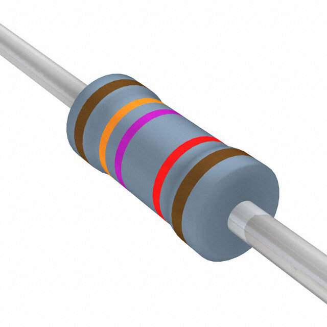
| 产品图片 |
|
| rohs | 符合RoHS无铅 / 符合限制有害物质指令(RoHS)规范要求 |
| 产品系列 | 逻辑集成电路,缓冲器和线路驱动器,NXP Semiconductors 74HCT240N,65274HCT |
| 数据手册 | |
| 产品型号 | 74HCT240N,652 |
| PCN封装 | |
| PCN组件/产地 | |
| 产品培训模块 | http://www.digikey.cn/PTM/IndividualPTM.page?site=cn&lang=zhs&ptm=24983 |
| 产品种类 | 缓冲器和线路驱动器 |
| 传播延迟时间 | 9 ns |
| 低电平输出电流 | 6 mA |
| 供应商器件封装 | 20-DIP |
| 元件数 | 2 |
| 其它名称 | 568-1527-5 |
| 包装 | 管件 |
| 商标 | NXP Semiconductors |
| 安装类型 | 通孔 |
| 安装风格 | Through Hole |
| 封装 | Tube |
| 封装/外壳 | 20-DIP(0.300",7.62mm) |
| 封装/箱体 | DIP-20 (SOT-146) |
| 工作温度 | -40°C ~ 125°C |
| 工厂包装数量 | 720 |
| 最大功率耗散 | 750 mW |
| 最大工作温度 | + 125 C |
| 最小工作温度 | - 40 C |
| 极性 | Inverting |
| 标准包装 | 18 |
| 每元件位数 | 4 |
| 每芯片的通道数量 | 8 |
| 电压-电源 | 4.5 V ~ 5.5 V |
| 电流-输出高,低 | 6mA,6mA |
| 电源电压-最大 | 5.5 V |
| 电源电压-最小 | 4.5 V |
| 输入线路数量 | 10 |
| 输出类型 | 3-State |
| 输出线路数量 | 8 |
| 逻辑类型 | Buffer/Line Driver |
| 逻辑系列 | HCT |
| 零件号别名 | 74HCT240N |
| 高电平输出电流 | - 6 mA |


PDF Datasheet 数据手册内容提取
74HC240; 74HCT240 Octal buffer/line driver; 3-state; inverting Rev. 03 — 2 August 2007 Product data sheet 1. General description The 74HC240; 74HCT240 is a high-speed Si-gate CMOS device and is pin compatible with Low-Power Schottky TTL (LSTTL). The 74HC240; 74HCT240 is a dual octal inverting buffer/line driver with 3-state outputs. The 3-state outputs are controlled by the output enable inputs 1OE and 2OE. A HIGH on nOE causes the outputs to assume a high impedance OFF-state. The 74HC240; 74HCT240 is similar to the 74HC244; 74HCT244 but has inverting outputs. 2. Features n Inverting 3-state outputs n Multiple package options n Complies with JEDEC standard no. 7 A n ESD protection: u HBMJESD22-A114-D exceeds 2000V u MMJESD22-A115-A exceeds 200V n Specified from- 40(cid:176) Cto+85(cid:176) C and from- 40(cid:176) Cto+125(cid:176) C 3. Ordering information Table 1. Ordering information Type number Package Temperature range Name Description Version 74HC240 74HC240N - 40(cid:176) C to +125(cid:176) C DIP20 plastic dual in-line package; 20leads (300 mil) SOT146-1 74HC240D - 40(cid:176) C to +125(cid:176) C SO20 plastic small outline package; 20leads; SOT163-1 bodywidth7.5mm 74HC240DB - 40(cid:176) C to +125(cid:176) C SSOP20 plastic shrink small outline package; 20leads; SOT339-1 body width 5.3mm 74HC240PW - 40(cid:176) C to +125(cid:176) C TSSOP20 plastic thin shrink small outline package; 20leads; SOT360-1 body width 4.4mm 74HC240BQ - 40(cid:176) C to +125(cid:176) C DHVQFN20 plastic dual-in-line compatible thermal enhanced SOT764-1 verythinquadflatpackage;noleads;20terminals; body 2.5· 4.5· 0.85mm 74HCT240 74HCT240N - 40(cid:176) C to +125(cid:176) C DIP20 plastic dual in-line package; 20leads (300 mil) SOT146-1
74HC240; 74HCT240 NXP Semiconductors Octal buffer/line driver; 3-state; inverting Table 1. Ordering information …continued Type number Package Temperature range Name Description Version 74HCT240D - 40(cid:176) C to +125(cid:176) C SO20 plastic small outline package; 20leads; SOT163-1 bodywidth7.5mm 74HCT240DB - 40(cid:176) C to +125(cid:176) C SSOP20 plastic shrink small outline package; 20leads; SOT339-1 body width 5.3mm 74HCT240PW - 40(cid:176) C to +125(cid:176) C TSSOP20 plastic thin shrink small outline package; 20leads; SOT360-1 body width 4.4mm 74HCT240BQ - 40(cid:176) C to +125(cid:176) C DHVQFN20 plastic dual-in-line compatible thermal enhanced SOT764-1 verythinquadflatpackage;noleads;20terminals; body 2.5· 4.5· 0.85mm 4. Functional diagram 2 1A0 1Y0 18 4 1A1 1Y1 16 6 1A2 1Y2 14 1 8 1A3 1Y3 12 EN 1 1OE 2 18 4 16 2 1A0 1Y0 18 17 2A0 2Y0 3 17 2A0 2Y0 3 6 14 8 12 4 1A1 1Y1 16 15 2A1 2Y1 5 15 2A1 2Y1 5 19 EN 13 2A2 2Y2 7 6 1A2 1Y2 14 13 2A2 2Y2 7 11 9 11 2A3 2Y3 9 8 1A3 1Y3 12 13 7 11 2A3 2Y3 9 15 5 19 2OE 1 1OE 17 3 19 2OE mgu779 mgu778 mgu780 Fig 1. Logic symbol Fig 2. IEC logic symbol Fig 3. Functional diagram 74HC_HCT240_3 © NXP B.V. 2007. All rights reserved. Product data sheet Rev. 03 — 2 August 2007 2 of 18
74HC240; 74HCT240 NXP Semiconductors Octal buffer/line driver; 3-state; inverting 5. Pinning information 5.1 Pinning 74HC240 74HCT240 terminal 1 OE CC index area 1 V 74HC240 1 20 74HCT240 1A0 2 19 2OE 2Y0 3 18 1Y0 1OE 1 20 VCC 1A1 4 17 2A0 1A0 2 19 2OE 2Y0 3 18 1Y0 2Y1 5 16 1Y1 1A1 4 17 2A0 1A2 6 15 2A1 2Y1 5 16 1Y1 2Y2 7 14 1Y2 1A2 6 15 2A1 1A3 8 GND(1) 13 2A2 2Y2 7 14 1Y2 2Y3 9 12 1Y3 1A3 8 13 2A2 0 1 1 1 2Y3 9 12 1Y3 D 3 GND 10 11 2A3 GN 2A 001aag234 001aag233 Transparent top view (1) The die substrate is attached to this pad using conductivedieattachmaterial.Itcannotbeusedas supply pin or input Fig 4. Pin configuration DIP20, SO20, (T)SSOP20 Fig 5. Pin configuration DHVQFN20 5.2 Pin description Table 2. Pin description Symbol Pin Description 1OE 1 output enable input (active LOW) 1A0 2 data input 2Y0 3 bus output 1A1 4 data input 2Y1 5 bus output 1A2 6 data input 2Y2 7 bus output 1A3 8 data input 2Y3 9 bus output GND 10 ground (0V) 2A3 11 data input 1Y3 12 bus output 2A2 13 data input 1Y2 14 bus output 2A1 15 data input 1Y1 16 bus output 74HC_HCT240_3 © NXP B.V. 2007. All rights reserved. Product data sheet Rev. 03 — 2 August 2007 3 of 18
74HC240; 74HCT240 NXP Semiconductors Octal buffer/line driver; 3-state; inverting Table 2. Pin description …continued Symbol Pin Description 2A0 17 data input 1Y0 18 bus output 2OE 19 output enable input (active LOW) V 20 supply voltage CC 6. Functional description Table 3. Function table[1] Input Output nOE nAn nYn L L H L H L H X Z [1] H=HIGH voltage level; L=LOW voltage level; X=don’t care; Z=high-impedance OFF-state. 7. Limiting values Table 4. Limiting values In accordance with the Absolute Maximum Rating System (IEC 60134). Voltages are referenced to GND (ground = 0 V). Symbol Parameter Conditions Min Max Unit V supply voltage - 0.5 +7 V CC I input clamping current V <- 0.5V or V >V +0.5 V - – 20 mA IK I I CC I output clamping current V <- 0.5V or V >V +0.5V - – 20 mA OK O O CC I output current - 0.5V < V < V +0.5V - – 35 mA O O CC I supply current - 70 mA CC I ground current - 70 - mA GND T storage temperature - 65 +150 (cid:176) C stg P total power dissipation [1] tot DIP20 package - 750 mW SO20, SSOP20, TSSOP20 - 500 mW and DHVQFN20 packages [1] For DIP20 packages: above 70(cid:176) C, P derates linearly with 12mW/K. tot For SO20 packages: above 70(cid:176) C, P derates linearly with 8mW/K. tot For SSOP20 and TSSOP20 packages: above 60(cid:176) C, P derates linearly with 5.5mW/K. tot For DHVQFN20 packages: above 60(cid:176) C, P derates linearly with 4.5mW/K. tot 74HC_HCT240_3 © NXP B.V. 2007. All rights reserved. Product data sheet Rev. 03 — 2 August 2007 4 of 18
74HC240; 74HCT240 NXP Semiconductors Octal buffer/line driver; 3-state; inverting 8. Recommended operating conditions Table 5. Recommended operating conditions Symbol Parameter Conditions Min Typ Max Unit 74HC240 V supply voltage 2.0 5.0 6.0 V CC V input voltage 0 - V V I CC V output voltage 0 - V V O CC D t/D V input transition rise and fall rate V = 2.0 V - - 625 ns/V CC V = 4.5 V - 1.67 139 ns/V CC V = 6.0 V - - 83 ns/V CC T ambient temperature - 40 - +125 (cid:176) C amb 74HCT240 V supply voltage 4.5 5.0 5.5 V CC V input voltage 0 - V V I CC V output voltage 0 - V V O CC D t/D V input transition rise and fall rate V = 4.5 V - 1.67 139 ns/V CC T ambient temperature - 40 - +125 (cid:176) C amb 9. Static characteristics Table 6. Static characteristics At recommended operating conditions; voltages are referenced to GND (ground=0V). Symbol Parameter Conditions 25(cid:176) C - 40(cid:176) C to +85(cid:176) C - 40(cid:176) Cto+125(cid:176) C Unit Min Typ Max Min Max Min Max 74HC240 V HIGH-level V =2.0V 1.5 1.2 - 1.5 - 1.5 - V IH CC input voltage V =4.5V 3.15 2.4 - 3.15 - 3.15 - V CC V =6.0V 4.2 3.2 - 4.2 - 4.2 - V CC V LOW-level V =2.0V - 0.8 0.5 - 0.5 - 0.5 V IL CC input voltage V =4.5V - 2.1 1.35 - 1.35 - 1.35 V CC V =6.0V - 2.8 1.8 - 1.8 - 1.8 V CC V HIGH-level V =V orV OH I IH IL output voltage I =- 20m A; V =2.0V 1.9 2.0 - 1.9 - 1.9 - V O CC I =- 20m A; V =4.5V 4.4 4.5 - 4.4 - 4.4 - V O CC I =- 20m A; V =6.0V 5.9 6.0 - 5.9 - 5.9 - V O CC I =- 6.0mA; V =4.5V 3.98 4.32 - 3.84 - 3.7 - V O CC I =- 7.8mA; V =6.0V 5.48 5.81 - 5.34 - 5.2 - V O CC 74HC_HCT240_3 © NXP B.V. 2007. All rights reserved. Product data sheet Rev. 03 — 2 August 2007 5 of 18
74HC240; 74HCT240 NXP Semiconductors Octal buffer/line driver; 3-state; inverting Table 6. Static characteristics …continued At recommended operating conditions; voltages are referenced to GND (ground=0V). Symbol Parameter Conditions 25(cid:176) C - 40(cid:176) C to +85(cid:176) C - 40(cid:176) Cto+125(cid:176) C Unit Min Typ Max Min Max Min Max V LOW-level V =V orV OL I IH IL output voltage I =20m A; V =2.0V - 0 0.1 - 0.1 - 0.1 V O CC I =20m A; V =4.5V - 0 0.1 - 0.1 - 0.1 V O CC I =20m A; V =6.0V - 0 0.1 - 0.1 - 0.1 V O CC I =6.0mA; V =4.5V - 0.15 0.26 - 0.33 - 0.4 V O CC I =7.8mA; V =6.0V - 0.16 0.26 - 0.33 - 0.4 V O CC I input leakage V =V orGND; - - – 0.1 - – 1.0 - – 1.0 m A I I CC current V =6.0V CC I OFF-state perinputpin;V =V orV ; - - – 0.5 - – 5.0 - – 10 m A OZ I IH IL output current V =V or GND; O CC otherinputsatV orGND; CC V =6.0V; I =0A CC O I supply current V =V orGND; I =0A; - - 8.0 - 80 - 160 m A CC I CC O V =6.0V CC C input - 3.5 - - - - - pF I capacitance 74HCT240 V HIGH-level V =4.5V to 5.5V 2.0 1.6 - 2.0 - 2.0 - V IH CC input voltage V LOW-level V =4.5V to 5.5V - 1.2 0.8 - 0.8 - 0.8 V IL CC input voltage V HIGH-level V =V orV ; V =4.5V OH I IH IL CC output voltage I =- 20m A 4.4 4.5 - 4.4 - 4.4 - V O I =- 6mA 3.98 4.32 - 3.84 - 3.7 - V O V LOW-level V =V orV ; V =4.5V OL I IH IL CC output voltage I =20m A - 0 0.1 - 0.1 - 0.1 V O I =6.0mA - 0.16 0.26 - 0.33 - 0.4 V O I input leakage V =V orGND; - - – 0.1 - – 1.0 - – 1.0 m A I I CC current V =5.5V CC I OFF-state perinputpin;V =V orV ; - - – 0.5 - – 5.0 - – 10 m A OZ I IH IL output current V =V or GND; O CC otherinputsatV orGND; CC V =5.5V; I =0A CC O I supply current V =V orGND; - - 8.0 - 80 - 160 m A CC I CC V =5.5V; I =0A CC O D I additional per input pin; CC supply current V =V - 2.1V; I CC otherinputsatV orGND; CC V =4.5Vto5.5V; CC I =0A O nAn or inputs - 150 540 - 675 - 735 m A nOE input - 70 252 - 315 - 343 m A C input - 3.5 - - - - - pF I capacitance 74HC_HCT240_3 © NXP B.V. 2007. All rights reserved. Product data sheet Rev. 03 — 2 August 2007 6 of 18
74HC240; 74HCT240 NXP Semiconductors Octal buffer/line driver; 3-state; inverting 10. Dynamic characteristics Table 7. Dynamic characteristics GND=0V; for load circuit seeFigure8. Symbol Parameter Conditions 25(cid:176) C - 40(cid:176) C to +125(cid:176) C Unit Min Typ Max Max Max (85(cid:176) C) (125(cid:176) C) 74HC240 t propagation delay nAn to nYn; [1] pd seeFigure6 V = 2.0 V - 30 100 125 150 ns CC V = 4.5 V - 11 20 25 30 ns CC V = 5.0 V; C =15pF - 9 - - - ns CC L V = 6.0 V - 9 17 21 26 ns CC t enable time nOE to nYn; seeFigure7 [2] en V = 2.0 V - 39 150 190 225 ns CC V = 4.5 V - 14 30 38 45 ns CC V = 6.0 V - 11 26 33 38 ns CC t disable time nOE to nYn or seeFigure7 [3] dis V = 2.0 V - 41 150 190 225 ns CC V = 4.5 V - 15 30 38 45 ns CC V = 6.0 V - 12 26 33 38 ns CC t transition time seeFigure6 [4] t V = 2.0 V - 14 60 75 90 ns CC V = 4.5 V - 5 12 15 18 ns CC V = 6.0 V - 4 10 13 15 ns CC C power dissipation per transceiver; [5] - 30 - - - pF PD capacitance V =GNDtoV I CC 74HC_HCT240_3 © NXP B.V. 2007. All rights reserved. Product data sheet Rev. 03 — 2 August 2007 7 of 18
74HC240; 74HCT240 NXP Semiconductors Octal buffer/line driver; 3-state; inverting Table 7. Dynamic characteristics …continued GND=0V; for load circuit seeFigure8. Symbol Parameter Conditions 25(cid:176) C - 40(cid:176) C to +125(cid:176) C Unit Min Typ Max Max Max (85(cid:176) C) (125(cid:176) C) 74HCT240 t propagation delay nAn to nYn; [1] pd seeFigure6 V = 4.5 V - 11 20 25 30 ns CC V = 5.0 V; C =15pF - 9 - - - ns CC L t enable time nOE to nYn; V =4.5 V; see [2] - 13 30 38 45 ns en CC Figure7 t disable time nOE to nYn; V =4.5 V; see [3] - 13 25 31 38 ns dis CC Figure7 t transition time V = 4.5 V; seeFigure6 [4] - 5 12 15 18 ns t CC C power dissipation per transceiver; [5] - 30 - - - pF PD capacitance V =GNDtoV - 1.5V I CC [1] t is the same as t and t . pd PHL PLH [2] t is the same as t and t . en PZH PZL [3] t is the same as t and t . dis PHZ PLZ [4] t is the same as t and t . t THL TLH [5] C is used to determine the dynamic power dissipation (P inm W): PD D P =C · V 2· f · N+(cid:229) (C · V 2· f ) where: D PD CC i L CC o f =input frequency in MHz; i f =output frequency in MHz; o C =output load capacitance in pF; L V =supply voltage in V; CC N=number of inputs switching; (cid:229) (C · V 2· f )=sum of outputs. L CC o 11. Waveforms VI nAn input VM VM GND tPHL tPLH VOH nYn output VM VM VOL mgu781 Measurement points are given inTable8. V and V are typical voltage output drop that occur with the output load. OL OH Fig 6. Input (nAn) to output (nYn) propagation delays and output transition times 74HC_HCT240_3 © NXP B.V. 2007. All rights reserved. Product data sheet Rev. 03 — 2 August 2007 8 of 18
74HC240; 74HCT240 NXP Semiconductors Octal buffer/line driver; 3-state; inverting VI nOE input VM GND tPLZ tPZL VCC nYn output LOW-to-OFF VM OFF-to-LOW VOL VX tPHZ tPZH nYn output VOH VY HIGH-to-OFF VM OFF-to-HIGH GND outputs outputs outputs enabled disabled enabled 001aae014 Measurement points are given inTable8. V and V are typical voltage output drop that occur with the output load. OL OH Fig 7. 3-state enable and disable times Table 8. Measurement points Type Input Output V V V V M M X Y 74HC240 0.5· V 0.5· V 0.1· V 0.9· V CC CC CC CC 74HCT240 1.3V 1.3V 0.1· V 0.9· V CC CC 74HC_HCT240_3 © NXP B.V. 2007. All rights reserved. Product data sheet Rev. 03 — 2 August 2007 9 of 18
74HC240; 74HCT240 NXP Semiconductors Octal buffer/line driver; 3-state; inverting tW VI 90 % negative pulse VM VM 10 % 0 V tf tr tr tf VI 90 % positive pulse VM VM 10 % 0 V tW VCC VCC PULSE VI VO RL S1 DUT open GENERATOR RT CL 001aad983 Test data is given inTable9. Definitions test circuit: R = Termination resistance should be equal to output impedance Z of the pulse generator. T o C = Load capacitance including jig and probe capacitance. L R = Load resistance. L S1 = Test selection switch. Fig 8. Load circuitry for measuring switching times Table 9. Test data Type Input Load S1 position V t, t C R t , t t , t t , t I r f L L PHL PLH PZH PHZ PZL PLZ 74HC240 V 6ns 15pF, 50 pF 1kW open GND V CC CC 74HCT240 3V 6ns 15pF, 50 pF 1kW open GND V CC 74HC_HCT240_3 © NXP B.V. 2007. All rights reserved. Product data sheet Rev. 03 — 2 August 2007 10 of 18
74HC240; 74HCT240 NXP Semiconductors Octal buffer/line driver; 3-state; inverting 12. Package outline DIP20: plastic dual in-line package; 20 leads (300 mil) SOT146-1 D ME e n a pl g n eati A2 A s L A1 c Z e w M b1 (e ) 1 b 20 11 MH pin 1 index E 1 10 0 5 10 mm scale DIMENSIONS (inch dimensions are derived from the original mm dimensions) UNIT mAax. mAi n1 . mAa 2x . b b1 c D(1) E(1) e e1 L ME MH w mZax(1.) 1.73 0.53 0.36 26.92 6.40 3.60 8.25 10.0 mm 4.2 0.51 3.2 2.54 7.62 0.254 2 1.30 0.38 0.23 26.54 6.22 3.05 7.80 8.3 0.068 0.021 0.014 1.060 0.25 0.14 0.32 0.39 inches 0.17 0.02 0.13 0.1 0.3 0.01 0.078 0.051 0.015 0.009 1.045 0.24 0.12 0.31 0.33 Note 1. Plastic or metal protrusions of 0.25 mm (0.01 inch) maximum per side are not included. OUTLINE REFERENCES EUROPEAN ISSUE DATE VERSION IEC JEDEC JEITA PROJECTION 99-12-27 SOT146-1 MS-001 SC-603 03-02-13 Fig 9. Package outline SOT146-1 (DIP20) 74HC_HCT240_3 © NXP B.V. 2007. All rights reserved. Product data sheet Rev. 03 — 2 August 2007 11 of 18
74HC240; 74HCT240 NXP Semiconductors Octal buffer/line driver; 3-state; inverting SO20: plastic small outline package; 20 leads; body width 7.5 mm SOT163-1 D E A X c y HE v M A Z 20 11 Q A2 A A1 (A 3 ) pin 1 index q Lp L 1 10 detail X e w M bp 0 5 10 mm scale DIMENSIONS (inch dimensions are derived from the original mm dimensions) UNIT mAax. A1 A2 A3 bp c D(1) E(1) e HE L Lp Q v w y Z(1) q 0.3 2.45 0.49 0.32 13.0 7.6 10.65 1.1 1.1 0.9 mm 2.65 0.25 1.27 1.4 0.25 0.25 0.1 0.1 2.25 0.36 0.23 12.6 7.4 10.00 0.4 1.0 0.4 8o 0.012 0.096 0.019 0.013 0.51 0.30 0.419 0.043 0.043 0.035 0o inches 0.1 0.01 0.05 0.055 0.01 0.01 0.004 0.004 0.089 0.014 0.009 0.49 0.29 0.394 0.016 0.039 0.016 Note 1. Plastic or metal protrusions of 0.15 mm (0.006 inch) maximum per side are not included. OUTLINE REFERENCES EUROPEAN ISSUE DATE VERSION IEC JEDEC JEITA PROJECTION 99-12-27 SOT163-1 075E04 MS-013 03-02-19 Fig 10. Package outline SOT163-1 (SO20) 74HC_HCT240_3 © NXP B.V. 2007. All rights reserved. Product data sheet Rev. 03 — 2 August 2007 12 of 18
74HC240; 74HCT240 NXP Semiconductors Octal buffer/line driver; 3-state; inverting SSOP20: plastic shrink small outline package; 20 leads; body width 5.3 mm SOT339-1 D E A X c y HE v M A Z 20 11 Q A2 A A1 (A 3 ) pin 1 index q Lp L 1 10 detail X w M e bp 0 2.5 5 mm scale DIMENSIONS (mm are the original dimensions) UNIT mAax. A1 A2 A3 bp c D(1) E(1) e HE L Lp Q v w y Z(1) q mm 2 00..2015 11..8605 0.25 00..3285 00..2009 77..40 55..42 0.65 77..96 1.25 10..0633 00..97 0.2 0.13 0.1 00..95 80oo Note 1. Plastic or metal protrusions of 0.2 mm maximum per side are not included. OUTLINE REFERENCES EUROPEAN ISSUE DATE VERSION IEC JEDEC JEITA PROJECTION 99-12-27 SOT339-1 MO-150 03-02-19 Fig 11. Package outline SOT339-1 (SSOP20) 74HC_HCT240_3 © NXP B.V. 2007. All rights reserved. Product data sheet Rev. 03 — 2 August 2007 13 of 18
74HC240; 74HCT240 NXP Semiconductors Octal buffer/line driver; 3-state; inverting TSSOP20: plastic thin shrink small outline package; 20 leads; body width 4.4 mm SOT360-1 D E A X c y HE v M A Z 20 11 Q A2 (A 3 ) A pin 1 index A1 q Lp L 1 10 detail X w M e bp 0 2.5 5 mm scale DIMENSIONS (mm are the original dimensions) UNIT mAax. A1 A2 A3 bp c D(1) E(2) e HE L Lp Q v w y Z(1) q mm 1.1 00..1055 00..9850 0.25 00..3109 00..21 66..64 44..53 0.65 66..62 1 00..7550 00..43 0.2 0.13 0.1 00..52 80oo Notes 1. Plastic or metal protrusions of 0.15 mm maximum per side are not included. 2. Plastic interlead protrusions of 0.25 mm maximum per side are not included. OUTLINE REFERENCES EUROPEAN ISSUE DATE VERSION IEC JEDEC JEITA PROJECTION 99-12-27 SOT360-1 MO-153 03-02-19 Fig 12. Package outline SOT360-1 (TSSOP20) 74HC_HCT240_3 © NXP B.V. 2007. All rights reserved. Product data sheet Rev. 03 — 2 August 2007 14 of 18
74HC240; 74HCT240 NXP Semiconductors Octal buffer/line driver; 3-state; inverting DHVQFN20: plastic dual in-line compatible thermal enhanced very thin quad flat package; no leads; 20 terminals; body 2.5 x 4.5 x 0.85 mm SOT764-1 D B A A A1 E c terminal 1 detail X index area terminal 1 e1 C index area e b v M C A B y1 C y w M C 2 9 L 1 10 Eh e 20 11 19 12 Dh X 0 2.5 5 mm scale DIMENSIONS (mm are the original dimensions) A(1) UNIT max. A1 b c D(1) Dh E(1) Eh e e1 L v w y y1 0.05 0.30 4.6 3.15 2.6 1.15 0.5 mm 1 0.2 0.5 3.5 0.1 0.05 0.05 0.1 0.00 0.18 4.4 2.85 2.4 0.85 0.3 Note 1. Plastic or metal protrusions of 0.075 mm maximum per side are not included. OUTLINE REFERENCES EUROPEAN ISSUE DATE VERSION IEC JEDEC JEITA PROJECTION 02-10-17 SOT764-1 - - - MO-241 - - - 03-01-27 Fig 13. Package outline SOT764-1 (DHVQFN20) 74HC_HCT240_3 © NXP B.V. 2007. All rights reserved. Product data sheet Rev. 03 — 2 August 2007 15 of 18
74HC240; 74HCT240 NXP Semiconductors Octal buffer/line driver; 3-state; inverting 13. Abbreviations Table 10. Abbreviations Acronym Description CMOS Complementary Metal Oxide Semiconductor DUT Device Under Test ESD ElectroStatic Discharge HBM Human Body Model MM Machine Model TTL Transistor-Transistor Logic 14. Revision history Table 11. Revision history Document ID Release date Data sheet status Change notice Supersedes 74HC_HCT240_3 20070802 Product data sheet - 74HC_HCT240_CNV_2 Modifications: • The format of this data sheet has been redesigned to comply with the new identity guidelines of NXP Semiconductors. • Legal texts have been adapted to the new company name where appropriate. • Added type number 74HC240BQ and 74HCT240BQ (DHVQFN20 package) 74HC_HCT240_CNV_2 19970828 Product specification - - 74HC_HCT240_3 © NXP B.V. 2007. All rights reserved. Product data sheet Rev. 03 — 2 August 2007 16 of 18
74HC240; 74HCT240 NXP Semiconductors Octal buffer/line driver; 3-state; inverting 15. Legal information 15.1 Data sheet status Document status[1][2] Product status[3] Definition Objective [short] data sheet Development This document contains data from the objective specification for product development. Preliminary [short] data sheet Qualification This document contains data from the preliminary specification. Product [short] data sheet Production This document contains the product specification. [1] Please consult the most recently issued document before initiating or completing a design. [2] The term ‘short data sheet’ is explained in section “Definitions”. [3] Theproductstatusofdevice(s)describedinthisdocumentmayhavechangedsincethisdocumentwaspublishedandmaydifferincaseofmultipledevices.Thelatestproductstatus information is available on the Internet at URLhttp://www.nxp.com. 15.2 Definitions malfunctionofaNXPSemiconductorsproductcanreasonablybeexpectedto result in personal injury, death or severe property or environmental damage. NXP Semiconductors accepts no liability for inclusion and/or use of NXP Draft —The document is a draft version only. The content is still under Semiconductors products in such equipment or applications and therefore internal review and subject to formal approval, which may result in such inclusion and/or use is at the customer’s own risk. modifications or additions. NXP Semiconductors does not give any representations or warranties as to the accuracy or completeness of Applications —Applications that are described herein for any of these informationincludedhereinandshallhavenoliabilityfortheconsequencesof products are for illustrative purposes only. NXP Semiconductors makes no use of such information. representation or warranty that such applications will be suitable for the specified use without further testing or modification. Short data sheet —A short data sheet is an extract from a full data sheet withthesameproducttypenumber(s)andtitle.Ashortdatasheetisintended Limiting values —Stress above one or more limiting values (as defined in forquickreferenceonlyandshouldnotbereliedupontocontaindetailedand theAbsoluteMaximumRatingsSystemofIEC60134)maycausepermanent full information. For detailed and full information see the relevant full data damagetothedevice.Limitingvaluesarestressratingsonlyandoperationof sheet, which is available on request via the local NXP Semiconductors sales the device at these or any other conditions above those given in the office. In case of any inconsistency or conflict with the short data sheet, the Characteristics sections of this document is not implied. Exposure to limiting full data sheet shall prevail. values for extended periods may affect device reliability. Terms and conditions of sale —NXP Semiconductors products are sold 15.3 Disclaimers subjecttothegeneraltermsandconditionsofcommercialsale,aspublished athttp://www.nxp.com/profile/terms, including those pertaining to warranty, intellectual property rights infringement and limitation of liability, unless General —Information in this document is believed to be accurate and explicitly otherwise agreed to in writing by NXP Semiconductors. In case of reliable.However,NXPSemiconductorsdoesnotgiveanyrepresentationsor any inconsistency or conflict between information in this document and such warranties,expressedorimplied,astotheaccuracyorcompletenessofsuch terms and conditions, the latter will prevail. information and shall have no liability for the consequences of use of such No offer to sell or license —Nothing in this document may be interpreted information. or construed as an offer to sell products that is open for acceptance or the Right to make changes —NXPSemiconductorsreservestherighttomake grant,conveyanceorimplicationofanylicenseunderanycopyrights,patents changes to information published in this document, including without or other industrial or intellectual property rights. limitation specifications and product descriptions, at any time and without notice.Thisdocumentsupersedesandreplacesallinformationsuppliedprior to the publication hereof. 15.4 Trademarks Suitability for use —NXP Semiconductors products are not designed, Notice:Allreferencedbrands,productnames,servicenamesandtrademarks authorized or warranted to be suitable for use in medical, military, aircraft, are the property of their respective owners. space or life support equipment, nor in applications where failure or 16. Contact information For additional information, please visit:http://www.nxp.com For sales office addresses, send an email to:salesaddresses@nxp.com 74HC_HCT240_3 © NXP B.V. 2007. All rights reserved. Product data sheet Rev. 03 — 2 August 2007 17 of 18
74HC240; 74HCT240 NXP Semiconductors Octal buffer/line driver; 3-state; inverting 17. Contents 1 General description. . . . . . . . . . . . . . . . . . . . . . 1 2 Features . . . . . . . . . . . . . . . . . . . . . . . . . . . . . . . 1 3 Ordering information. . . . . . . . . . . . . . . . . . . . . 1 4 Functional diagram . . . . . . . . . . . . . . . . . . . . . . 2 5 Pinning information. . . . . . . . . . . . . . . . . . . . . . 3 5.1 Pinning . . . . . . . . . . . . . . . . . . . . . . . . . . . . . . . 3 5.2 Pin description . . . . . . . . . . . . . . . . . . . . . . . . . 3 6 Functional description . . . . . . . . . . . . . . . . . . . 4 7 Limiting values. . . . . . . . . . . . . . . . . . . . . . . . . . 4 8 Recommended operating conditions. . . . . . . . 5 9 Static characteristics. . . . . . . . . . . . . . . . . . . . . 5 10 Dynamic characteristics . . . . . . . . . . . . . . . . . . 7 11 Waveforms . . . . . . . . . . . . . . . . . . . . . . . . . . . . . 8 12 Package outline . . . . . . . . . . . . . . . . . . . . . . . . 11 13 Abbreviations. . . . . . . . . . . . . . . . . . . . . . . . . . 16 14 Revision history. . . . . . . . . . . . . . . . . . . . . . . . 16 15 Legal information. . . . . . . . . . . . . . . . . . . . . . . 17 15.1 Data sheet status . . . . . . . . . . . . . . . . . . . . . . 17 15.2 Definitions. . . . . . . . . . . . . . . . . . . . . . . . . . . . 17 15.3 Disclaimers. . . . . . . . . . . . . . . . . . . . . . . . . . . 17 15.4 Trademarks. . . . . . . . . . . . . . . . . . . . . . . . . . . 17 16 Contact information. . . . . . . . . . . . . . . . . . . . . 17 17 Contents. . . . . . . . . . . . . . . . . . . . . . . . . . . . . . 18 Pleasebeawarethatimportantnoticesconcerningthisdocumentandtheproduct(s) described herein, have been included in section ‘Legal information’. © NXP B.V. 2007. All rights reserved. For more information, please visit: http://www.nxp.com For sales office addresses, please send an email to: salesaddresses@nxp.com Date of release: 2 August 2007 Document identifier: 74HC_HCT240_3