ICGOO在线商城 > 集成电路(IC) > 接口 - 模拟开关,多路复用器,多路分解器 > 74HC4852PW,118
 Datasheet下载
- 型号: 74HC4852PW,118
- 制造商: NXP Semiconductors
- 库位|库存: xxxx|xxxx
- 要求:
| 数量阶梯 | 香港交货 | 国内含税 |
| +xxxx | $xxxx | ¥xxxx |
查看当月历史价格
查看今年历史价格
74HC4852PW,118产品简介:
ICGOO电子元器件商城为您提供74HC4852PW,118由NXP Semiconductors设计生产,在icgoo商城现货销售,并且可以通过原厂、代理商等渠道进行代购。 74HC4852PW,118价格参考¥3.24-¥3.24。NXP Semiconductors74HC4852PW,118封装/规格:接口 - 模拟开关,多路复用器,多路分解器, 2 Circuit IC Switch 4:1 195 Ohm 16-TSSOP。您可以下载74HC4852PW,118参考资料、Datasheet数据手册功能说明书,资料中有74HC4852PW,118 详细功能的应用电路图电压和使用方法及教程。
型号为 74HC4852PW,118 的芯片属于 Nexperia USA Inc. 旗下的 模拟开关/多路复用器/多路分解器 类产品,广泛应用于需要对模拟或数字信号进行切换和路由的场景。

该器件为 双路 4 通道模拟多路复用器/多路分解器(Dual 4:1 Multiplexer/Demultiplexer),采用 TSSOP 封装,适用于中高密度逻辑控制与信号路由。其主要应用场景包括:

1. 通信系统:用于信号路径选择,如在多路通信信道中选择一路进行传输或接收。
2. 测试与测量设备:在多路输入信号中切换,实现对不同信号源的测量与分析。
3. 工业控制:用于传感器信号的多路选择,实现PLC或控制系统中的信号路由。
4. 音频设备:用于音频信号的切换,如多路音频输入选择。
5. 数据采集系统:在多个传感器或数据源之间进行切换,共享同一数据处理通道。
6. 消费类电子产品:如电视、音响系统中用于输入选择或信号路径控制。

其低功耗、高速特性使其适用于电池供电设备和高频切换应用。
| 参数 | 数值 |
| 产品目录 | 集成电路 (IC) |
| 描述 | IC MUX/DEMUX DUAL 4X1 16TSSOP |
| 产品分类 | |
| 品牌 | NXP Semiconductors |
| 数据手册 | |
| 产品图片 |
|
| 产品型号 | 74HC4852PW,118 |
| PCN封装 | |
| PCN组件/产地 | |
| rohs | 无铅 / 符合限制有害物质指令(RoHS)规范要求 |
| 产品系列 | 74HC |
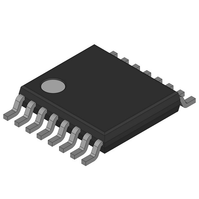
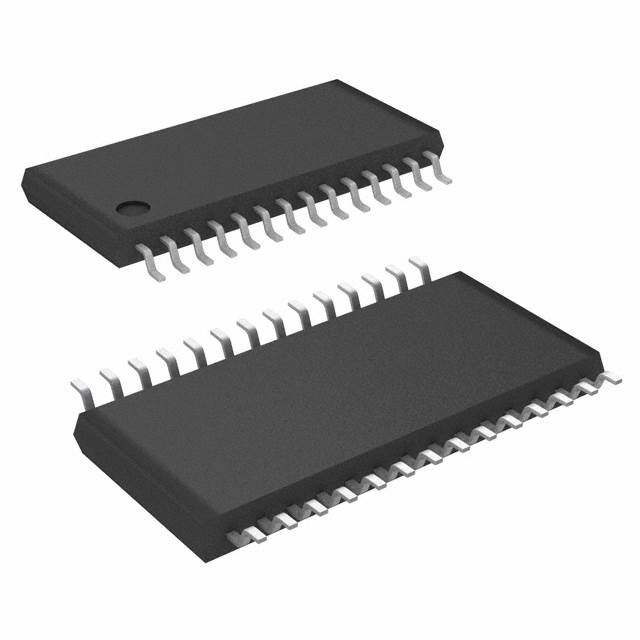
| 供应商器件封装 | 16-TSSOP |
| 其它名称 | 568-8891-1 |
| 功能 | 多路复用器/多路分解器 |
| 包装 | 剪切带 (CT) |
| 安装类型 | 表面贴装 |
| 导通电阻 | 195 欧姆 |
| 封装/外壳 | 16-TSSOP(0.173",4.40mm 宽) |
| 工作温度 | -40°C ~ 125°C |
| 标准包装 | 1 |
| 电压-电源,单/双 (±) | 2 V ~ 6 V |
| 电压源 | 单电源 |
| 电流-电源 | 2µA |
| 电路 | 2 x 4:1 |


- 商务部:美国ITC正式对集成电路等产品启动337调查
- 曝三星4nm工艺存在良率问题 高通将骁龙8 Gen1或转产台积电
- 太阳诱电将投资9.5亿元在常州建新厂生产MLCC 预计2023年完工
- 英特尔发布欧洲新工厂建设计划 深化IDM 2.0 战略
- 台积电先进制程称霸业界 有大客户加持明年业绩稳了
- 达到5530亿美元!SIA预计今年全球半导体销售额将创下新高
- 英特尔拟将自动驾驶子公司Mobileye上市 估值或超500亿美元
- 三星加码芯片和SET,合并消费电子和移动部门,撤换高东真等 CEO
- 三星电子宣布重大人事变动 还合并消费电子和移动部门
- 海关总署:前11个月进口集成电路产品价值2.52万亿元 增长14.8%


PDF Datasheet 数据手册内容提取
74HC4852; 74HCT4852 Dual 4-channel analog multiplexer/demultiplexer with injection-current effect control Rev. 03 — 2 September 2008 Product data sheet 1. General description The 74HC4852; 74HCT4852 are high-speed Si-gate CMOS devices and are specified in compliance with JEDEC standard no. 7A. The 74HC4852; 74HCT4852 are dual 4-channel analog multiplexers/demultiplexers with commonselectinputs(S0andS1).BothmultiplexershaveacommonactiveLOWenable input (E), four independent inputs/outputs (nY0 to nY3) and two common inputs/outputs (1Z, 2Z). The devices feature injection-current effect control, which has excellent value in automotive applications where voltages in excess of the supply voltage are common. WithE LOW, two of the eight switches are selected (low impedance ON-state) by S0 and S1. WithE HIGH, all switches are in the high-impedance OFF-state, independent of S0 and S1. The injection-current effect control allows signals at disabled analog input channels to exceedthesupplyvoltagewithoutaffectingthesignaloftheenabledanalogchannel.This eliminatestheneedforexternaldiode/resistornetworkstypicallyusedtokeeptheanalog channel signals within the supply-voltage range. 2. Features n Injection-current cross coupling < 1 mV/mA n Wide supply voltage range from 2.0 Vto6.0V for 74HC4852 n ESD protection: u HBM JESD22-A114E exceeds 2000V u CDM JESD22-C101C exceeds 1000V n Latch-up performance exceeds 100mA per JESD 78 Class II level A n Low ON-state resistance: u 400W (typical) at V =2.0V CC u 215W (typical) at V =3.0V CC u 120W (typical) at V =3.3V CC u 76W (typical) at V =4.5V CC u 59W (typical) at V =6.0V CC
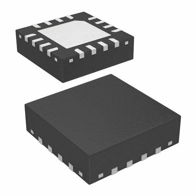
74HC4852; 74HCT4852 Nexperia 4-channel analog MUX/DEMUX with injection-current effect control 3. Applications n Analog multiplexing and demultiplexing n Digital multiplexing and demultiplexing n Signal gating n Automotive application 4. Ordering information Table 1. Ordering information Type number Package Temperature range Name Description Version 74HC4852D -40 (cid:176)Cto+125 (cid:176)C SO16 plastic small outline package; 16 leads; SOT109-1 bodywidth3.9mm 74HC4852PW -40 (cid:176)Cto+125 (cid:176)C TSSOP16 plastic thin shrink small outline package; 16 leads; SOT403-1 bodywidth4.4mm 74HC4852BQ -40 (cid:176)Cto+125 (cid:176)C DHVQFN16 plastic dual in-line compatible thermal enhanced very SOT763-1 thin quad flat package; no leads; 16 terminals; body2.5· 3.5· 0.85mm 74HCT4852D -40 (cid:176)Cto+125 (cid:176)C SO16 plastic small outline package; 16 leads; SOT109-1 bodywidth3.9mm 74HCT4852PW -40 (cid:176)Cto+125 (cid:176)C TSSOP16 plastic thin shrink small outline package; 16 leads; SOT403-1 bodywidth4.4mm 74HCT4852BQ -40 (cid:176)Cto+125 (cid:176)C DHVQFN16 plastic dual in-line compatible thermal enhanced very SOT763-1 thin quad flat package; no leads; 16 terminals; body2.5· 3.5· 0.85mm 5. Functional diagram 10 0 0 4 · 9 3 1 13 6 G4 1Z 1Y0 12 1Y1 14 MUX/DMUX 1 0 10 S0 1Y2 15 5 1 3 9 S1 1Y3 11 2 2 2Y0 1 3 4 2Y1 5 0 12 14 2Y2 2 13 1 15 6 E 2Y3 4 2 2Z 11 3 3 001aag093 001aag094 Fig 1. Logic symbol Fig 2. IEC logic symbol 74HC_HCT4852_3 © Nexperia B.V. 2017. All rights reserved Product data sheet Rev. 03 — 2 September 2008 2 of 20
74HC4852; 74HCT4852 Nexperia 4-channel analog MUX/DEMUX with injection-current effect control VCC 16 INJECTION 13 CURRENT 1Z CONTROL INJECTION 12 CURRENT 1Y0 CONTROL INJECTION 14 CURRENT 1Y1 CONTROL INJECTION 15 CURRENT 1Y2 10 CONTROL S0 INJECTION 11 1-OF-4 CURRENT 1Y3 DECODER CONTROL INJECTION 1 CURRENT 2Y0 9 CONTROL S1 INJECTION 5 CURRENT 2Y1 CONTROL INJECTION 2 CURRENT 2Y2 6 CONTROL E INJECTION 4 CURRENT 2Y3 CONTROL INJECTION 3 CURRENT 2Z CONTROL GND 8 001aag095 Fig 3. Functional diagram 74HC_HCT4852_3 © Nexperia B.V. 2017. All rights reserved Product data sheet Rev. 03 — 2 September 2008 3 of 20
74HC4852; 74HCT4852 Nexperia 4-channel analog MUX/DEMUX with injection-current effect control 6. Pinning information 6.1 Pinning 74HC4852 74HC4852 74HCT4852 74HCT4852 2Y0 1 16 VCC itnedrmexin aarle 1a 2Y0 VCC 2Y2 2 15 1Y2 1 16 2Y2 2 15 1Y2 2Z 3 14 1Y1 2Z 3 14 1Y1 2Y3 4 13 1Z 2Y3 4 13 1Z 2Y1 5 12 1Y0 2Y1 5 12 1Y0 E 6 GND(1) 11 1Y3 E 6 11 1Y3 n.c. 7 10 S0 n.c. 7 10 S0 8 9 D 1 GND 8 9 S1 GN S 001aag097 001aag096 Transparent top view (1) The die substrate is attached to this pad using conductivedieattachmaterial.Itcannotbeusedas a supply pin or input. Fig 4. Pin configuration SO16 and TSSOP16 Fig 5. Pin configuration DHVQFN16 6.2 Pin description Table 2. Pin description Symbol Pin Description 2Y0 1 independent input/output 2Y2 2 independent input/output 2Z 3 common input/output 2Y3 4 independent input/output 2Y1 5 independent input/output E 6 enable input (active LOW) n.c. 7 not connected GND 8 ground (0V) S1 9 select input S0 10 select input 1Y3 11 independent input/output 1Y0 12 independent input/output 1Z 13 common input/output 1Y1 14 independent input/output 1Y2 15 independent input/output V 16 supply voltage CC 74HC_HCT4852_3 © Nexperia B.V. 2017. All rights reserved Product data sheet Rev. 03 — 2 September 2008 4 of 20
74HC4852; 74HCT4852 Nexperia 4-channel analog MUX/DEMUX with injection-current effect control 7. Functional description Table 3. Function table[1] Input Channel ON E S1 S0 L L L nY0tonZ L L H nY1tonZ L H L nY2tonZ L H H nY3tonZ H X X - [1] H=HIGH voltage level; L=LOW voltage level; X=don’t care. 8. Limiting values Table 4. Limiting values In accordance with the Absolute Maximum Rating System (IEC 60134). Voltages are referenced to GND (ground=0V). Symbol Parameter Conditions Min Max Unit V supply voltage - 0.5 +7.0 V CC V input voltage [1] - 0.5 V +0.5 V I CC V switch voltage [2] - 0.5 V +0.5 V SW CC I input clamping current V <-0.5V or V >V + 0.5 V - –20 mA IK I I CC I switch clamping current V <-0.5V or V >V + 0.5 V - –20 mA SK SW SW CC I switch current V >-0.5V or V < V + 0.5 V - –25 mA SW SW SW CC I supply current - 50 mA CC I ground current - 50 - mA GND T storage temperature - 65 +150 (cid:176)C stg P total power dissipation T =-40 (cid:176)Cto+125 (cid:176)C [3] - 500 mW tot amb [1] The minimum and maximum input voltage rating may be exceeded if the input clamping current rating is observed. [2] The minimum and maximum switch voltage rating may be exceeded if the switch clamping current rating is observed. [3] For SO16 package: P derates linearly with 8mW/K above 70(cid:176)C. tot For TSSOP16 package: P derates linearly with 5.5mW/K above 60(cid:176)C. tot For DHVQFN16 packages: P derates linearly with 4.5mW/K above 60(cid:176)C. tot 74HC_HCT4852_3 © Nexperia B.V. 2017. All rights reserved Product data sheet Rev. 03 — 2 September 2008 5 of 20
74HC4852; 74HCT4852 Nexperia 4-channel analog MUX/DEMUX with injection-current effect control 9. Recommended operating conditions Table 5. Recommended operating conditions Symbol Parameter Conditions 74HC4852 74HCT4852 Unit Min Typ Max Min Typ Max V supply voltage 2.0 - 6.0 4.5 5.0 5.5 V CC V input voltage 0 - V 0 - V V I CC CC V switch voltage 0 - V 0 - V V SW CC CC T ambient temperature -40 - +125 -40 - +125 (cid:176)C amb Dt/DV input transition rise and V =2.0V - 6.0 1000 - - - ns/V CC fall rate V =3.0V - 6.0 800 - - - ns/V CC V =3.3V - 6.0 800 - - - ns/V CC V =4.5V - 6.0 500 - 6.0 500 ns/V CC V =6.0V - 6.0 400 - - - ns/V CC 10. Static characteristics Table 6. R ON resistance At recommended operating conditions; voltages are referenced to GND (ground 0V);For test circuit seeFigure8. Symbol Parameter Conditions 25(cid:176)C -40 (cid:176)C to +85 (cid:176)C -40 (cid:176)C to +125 (cid:176)C Unit Min Typ Max Min Max Min Max 74HC4852 R ONresistance V = V to GND;E = V ON(peak) I CC IL (peak) V = 2.0 V; I =2mA - 400 650 - 670 - 700 W CC SW V = 3.0 V; I £ 2mA - 215 330 - 360 - 380 W CC SW V = 3.3 V; I £ 2mA - 120 270 - 305 - 345 W CC SW V = 4.5 V; I £ 2mA - 76 210 - 240 - 270 W CC SW V = 6.0 V; I £ 2mA - 59 195 - 220 - 250 W CC SW DR ONresistance V = 0.5· V ;E = V ON I CC IL mismatch V = 2.0 V; I =2mA - 4 10 - 15 - 20 W CC SW between channels VCC = 3.0 V; ISW£ 2mA - 2 8 - 12 - 16 W V = 3.3 V; I £ 2mA - 2 8 - 12 - 16 W CC SW V = 4.5 V; I £ 2mA - 2 8 - 12 - 16 W CC SW V = 6.0 V; I £ 2mA - 3 9 - 13 - 18 W CC SW 74HCT4852 R ONresistance V = V to GND;E = V ON(peak) I CC IL (peak) V = 4.5 V; I £ 2mA - 76 210 - 240 - 270 W CC SW DR ONresistance V = 0.5· V ;E = V ON I CC IL mismatch V = 4.5 V; I £ 2mA - 2 8 - 12 - 16 W CC SW between channels 74HC_HCT4852_3 © Nexperia B.V. 2017. All rights reserved Product data sheet Rev. 03 — 2 September 2008 6 of 20
74HC4852; 74HCT4852 Nexperia 4-channel analog MUX/DEMUX with injection-current effect control Table 7. Injection current coupling At recommended operating conditions; voltages are referenced to GND (ground 0V);For test circuit seeFigure9. Symbol Parameter Conditions 74HC4852 74HCT4852 Unit Min Typ[1] Max Min Typ[1] Max T =-40 (cid:176)C to +125 (cid:176)C amb DV output voltage |I |£ 1 mA; R £ 3.9 k W [2][3] O SW S variation V = 3.3 V - 0.05 1 - - - mV CC V = 5.0 V - 0.03 1 - 0.03 1 mV CC |I |£ 10mA;R £ 3.9kW SW S V = 3.3 V - 0.55 5 - - - mV CC V = 5.0 V - 0.27 5 - 0.27 5 mV CC |I |£ 1 mA; R £ 20 kW SW S V = 3.3 V - 0.04 2 - - - mV CC V = 5.0 V - 0.03 2 - 0.03 2 mV CC |I |£ 10 mA; R £ 20 kW SW S V = 3.3 V - 0.56 20 - - - mV CC V = 5.0 V - 0.48 20 - 0.48 20 mV CC [1] Typical values are measured at T =25(cid:176)C. amb [2] D V here is the maximum variation of output voltage of an enabled analog channel when current is injected into any disabled channel. O [3] I = total current injected into all disabled channels. SW Table 8. Static characteristics At recommended operating conditions; voltages are referenced to GND (ground 0V). 25(cid:176)C -40 (cid:176)C to +85 (cid:176)C -40 (cid:176)C to +125 (cid:176)C Symbol Parameter Conditions Min Typ Max Min Max Min Max Unit 74HC4852 V HIGH-level control inputs IH input V = 2.0 V 1.5 - - 1.5 - 1.5 - V CC voltage V = 3.0 V 2.1 - - 2.1 - 2.1 - V CC V = 3.3 V 2.3 - - 2.3 - 2.3 - V CC V = 4.5 V 3.15 - - 3.15 - 3.15 - V CC V = 6.0 V 4.2 - - 4.2 - 4.2 - V CC V LOW-level control inputs IL input V = 2.0 V - - 0.5 - 0.5 - 0.5 V CC voltage V = 3.0 V - - 0.9 - 0.9 - 0.9 V CC V = 3.3 V - - 1.0 - 1.0 - 1.0 V CC V = 4.5 V - - 1.35 - 1.35 - 1.35 V CC V = 6.0 V - - 1.8 - 1.8 - 1.8 V CC I input control inputs; I leakage V =GNDorV I CC current V = 6.0 V - - –0.1 - –0.1 - –1.0 mA CC 74HC_HCT4852_3 © Nexperia B.V. 2017. All rights reserved Product data sheet Rev. 03 — 2 September 2008 7 of 20
74HC4852; 74HCT4852 Nexperia 4-channel analog MUX/DEMUX with injection-current effect control Table 8. Static characteristics …continued At recommended operating conditions; voltages are referenced to GND (ground 0V). 25(cid:176)C -40 (cid:176)C to +85 (cid:176)C -40 (cid:176)C to +125 (cid:176)C Symbol Parameter Conditions Min Typ Max Min Max Min Max Unit I OFF-state E = V ; V = GND or V ; S(OFF) IH I CC leakage V =V orGND; V = 6.0 O CC CC current V; seeFigure6 nYn; per channel - - –0.1 - –0.5 - –1.0 mA nZ; all channels - - –0.2 - –2.0 - –4.0 mA I ON-state E = V ; V = GND or V ; - - –0.1 - –0.5 - –1.0 mA S(ON) IL I CC leakage V =V orGND; V = 6.0 O CC CC current V; seeFigure7 I supply V = GND or V CC I CC current V = 6.0 V - - 2.0 - 5.0 - 20.0 mA CC C input S0, S1, S2 andE - 2 10 - 10 - 10 pF I capacitance C switch nZ; OFF-state - 15 40 - 40 - 40 pF sw capacitance nYn; OFF-state - 3 15 - 15 - 15 pF 74HCT4852 V HIGH-level control inputs IH input V = 4.5 V to 5.5 V 2.0 - - 2.0 - 2.0 - V CC voltage V LOW-level control inputs IL input V = 4.5 V to 5.5 V - - 0.8 - 0.8 - 0.8 V CC voltage I input control inputs; I leakage V =GNDorV I CC current V = 5.5 V - - –0.1 - –0.1 - –1.0 mA CC I OFF-state E = V ; V = GND or V ; S(OFF) IH I CC leakage V =V orGND; O CC current V =5.5V; seeFigure6 CC per channel - - –0.1 - –0.5 - –1.0 mA all channels - - –0.2 - –2.0 - –4.0 mA I ON-state E = V ; V = GND or V ; - - –0.1 - –0.5 - –1.0 mA S(ON) IL I CC leakage V =V orGND; O CC current V =5.5V; seeFigure7 CC I supply V = GND or V CC I CC current V = 5.5 V - - 2.0 - 5.0 - 20.0 mA CC DI additional control inputs; - - 300 - 370 - 370 mA CC supply V =V - 2.1V; I CC current otherinputsat V orGND; CC V =4.5Vto5.5V; I =0A CC O C input S0, S1, S2 andE - 2 10 - 10 - 10 pF I capacitance C switch nZ; OFF-state - 9 40 - 40 - 40 pF sw capacitance nYn; OFF-state - 3 15 - 15 - 15 pF 74HC_HCT4852_3 © Nexperia B.V. 2017. All rights reserved Product data sheet Rev. 03 — 2 September 2008 8 of 20
74HC4852; 74HCT4852 Nexperia 4-channel analog MUX/DEMUX with injection-current effect control VCC selected channel(1) nYn IS VI nZ n.c. VCC E E VIH VIL nYn nZ nYn IS IS any disabled channel VI GND VO VO GND 001aag098 001aag099 (1) Channel is selected by S0 and S1. Fig 6. Test circuit for measuring OFF-state leakage Fig 7. Test circuit for measuring ON-state leakage current current VCC any disabled channel VI(1) nYn ISW nZ VSW V E VCC VIL VIL E VI(2) nYn selected channel(1) nYn nZ RS GND VI GND ISW VI VO 001aag100 001aag101 R = V / I . (1) Channel is selected by S0 and S1. ON SW SW V(1) < GND or V(1) > V . I I CC GND < V(2) < V . I CC Fig 8. Test circuit for measuring ON resistance Fig 9. Test circuit for injection current coupling 74HC_HCT4852_3 © Nexperia B.V. 2017. All rights reserved Product data sheet Rev. 03 — 2 September 2008 9 of 20
74HC4852; 74HCT4852 Nexperia 4-channel analog MUX/DEMUX with injection-current effect control 11. Dynamic characteristics Table 9. Dynamic characteristics At recommended operating conditions; voltages are referenced to GND (ground 0V); for load circuit seeFigure14. Symbol Parameter Conditions 25(cid:176)C -40 (cid:176)C to+85 (cid:176)C -40 (cid:176)C to+125 (cid:176)C Unit Min Typ Max Min Max Min Max 74HC4852 t propagation delay nZ,nYntonYn,nZ; [1] pd seeFigure10 V = 2.0 V 2.2 9.3 33 2.2 34 2.2 35 ns CC V = 3.0 V 2.2 4.9 16.5 1.9 18 1.9 19.5 ns CC V = 3.3 V 2.0 4.4 15.0 1.6 16.5 1.6 18.5 ns CC V = 4.5 V 1.6 3.2 11.6 1.1 12.5 1.1 13.5 ns CC V = 6.0 V 1.5 2.5 10.2 0.9 11 0.9 12 ns CC SntonZ, nYn; [1] seeFigure11 V = 2.0 V 7.7 16.8 38 6.3 40 6.3 42 ns CC V = 3.0 V 4.9 8.8 20 3.9 21.5 3.9 23 ns CC V = 3.3 V 4.4 7.9 17.5 3.4 19 3.4 22 ns CC V = 4.5 V 3.2 5.8 14 2.3 15 2.3 17 ns CC V = 6.0 V 2.4 4.8 12.6 1.6 14.5 1.6 16.5 ns CC t enable time EtonZ,nYn; [2] en seeFigure12 V = 2.0 V 10.5 20.5 47.5 8.5 52.5 8.5 57.5 ns CC V = 3.0 V 6.2 10.6 45 5.2 50 5.2 55 ns CC V = 3.3 V 5.6 9.4 42.5 4.6 47.5 4.6 52.5 ns CC V = 4.5 V 4.2 6.9 40 3 45 3 50 ns CC V = 6.0 V 3.2 5.6 39 2.2 40 2.2 40 ns CC t disable time EtonZ,nYn; [3] dis seeFigure12 V = 2.0 V 39.5 75.4 100 39.3 105 39 115 ns CC V = 3.0 V 35.2 69.5 90 35.5 100 35 110 ns CC V = 3.3 V 34.6 68.1 85 34.6 95 34.5 105 ns CC V = 4.5 V 28.5 63 80 28.2 90 28 100 ns CC V = 6.0 V 14.4 57.9 78 13.5 80 13.0 80 ns CC C power dissipation per channel; [4] PD capacitance seeFigure13 V = 3.3V - 42 - - - - - pF CC V = 5.0V - 47 - - - - - pF CC 74HC_HCT4852_3 © Nexperia B.V. 2017. All rights reserved Product data sheet Rev. 03 — 2 September 2008 10 of 20
74HC4852; 74HCT4852 Nexperia 4-channel analog MUX/DEMUX with injection-current effect control Table 9. Dynamic characteristics …continued At recommended operating conditions; voltages are referenced to GND (ground 0V); for load circuit seeFigure14. Symbol Parameter Conditions 25(cid:176)C -40 (cid:176)C to+85 (cid:176)C -40 (cid:176)C to+125 (cid:176)C Unit Min Typ Max Min Max Min Max 74HCT4852 t propagation delay nZ,nYntonYn,nZ; [1] pd seeFigure10 V = 4.5 V 1.6 3.5 11.5 1.1 12.5 1.1 13.5 ns CC SntonZ, nYn; [1] seeFigure11 V = 4.5 V 3.2 7.6 13 2.3 15 1.6 17 ns CC t enable time EtonZ,nYn; [2] en seeFigure12 V = 4.5 V 4.2 8.3 25 3.0 30 3.0 35 ns CC t disable time EtonZ,nYn; [3] dis seeFigure12 V = 4.5 V 28.5 61.8 80 28.2 90 28.0 100 ns CC C power dissipation per channel; [4] PD capacitance seeFigure13 V = 5.0V - 47 - - - - - pF CC [1] t is the same as t and t . pd PLH PHL [2] t is the same as t and t . en PZH PZL [3] t is the same as t and t . dis PLZ PHZ [4] C is used to determine the dynamic power dissipation (P inm W): PD D P =C · V 2· f +(cid:229) {(C +C )· V 2· f } where: D PD CC i L sw CC o f =input frequency in MHz; i f =output frequency in MHz; o (cid:229) {(C +C )· V 2· f }=sum of outputs; L sw CC o C =output load capacitance in pF; L C = switch capacitance in pF; sw V =supply voltage in V. CC 12. Waveforms VCC nZ or nYn input 0.5VCC GND tPLH tPHL VCC nYn or nZ 0.5VCC output GND 001aah578 Fig 10. Input (nZ, nYn) to output (nYn, nZ) propagation delays 74HC_HCT4852_3 © Nexperia B.V. 2017. All rights reserved Product data sheet Rev. 03 — 2 September 2008 11 of 20
74HC4852; 74HCT4852 Nexperia 4-channel analog MUX/DEMUX with injection-current effect control VI Sn input VM GND tPLH tPHL VCC nYn or nZ output VM GND 001aah579 Measurement points are given inTable10. Fig 11. Input (Sn) to output (nYn, nZ) propagation delays VI E input VM VM 0 V tPLZ tPZL VCC nZ or nYn output VM VOL VX tPHZ tPZH VOH VY nZ or nYn output VM GND switch ON switch OFF switch ON 001aah580 Measurement points are shown inTable10. Logic levels: V and V are typical output voltage levels that occur with the output load. OL OH Fig 12. Enable and disable times Table 10. Measurement points Type Input Output V V V V V M I M X Y 74HC4852 0.5V V 0.5V V + 0.1(V - V ) 0.9V CC CC CC OL CC OL OH 74HCT4852 1.3V 3.0 V 0.5V V + 0.1(V - V ) 0.9V CC OL CC OL OH 74HC_HCT4852_3 © Nexperia B.V. 2017. All rights reserved Product data sheet Rev. 03 — 2 September 2008 12 of 20
74HC4852; 74HCT4852 Nexperia 4-channel analog MUX/DEMUX with injection-current effect control VCC A selected channel nYn G Sn nZ n.c. E nYn disabled channel GND 001aah581 Fig 13. Test circuit for measuring power dissipation capacitance 74HC_HCT4852_3 © Nexperia B.V. 2017. All rights reserved Product data sheet Rev. 03 — 2 September 2008 13 of 20
74HC4852; 74HCT4852 Nexperia 4-channel analog MUX/DEMUX with injection-current effect control tW VI 90 % 90 % negative pulse VM VM 10 % 0 V tf tr tr tf VI 90 % positive pulse VM VM 10 % 10 % 0 V tW 001aac221 a. Input pulse definition switch VCC VCC open RL VI VO G DUT RT CL GND 001aaf883 Definitions for test circuit: R = load resistance. L C =load capacitance including jig and probe capacitance. L R =termination resistance should be equal to the output impedance Z of the pulse generator. T o b. Load circuit Test data is given inTable11. Fig 14. Input pulse definition and load circuit Table 11. Test data Test Input Output S1 position ControlE, Sn Switch nYn (nZ) t, t Switch nZ (nYn) r f V[1] V C R I I L L t t V V 6ns 50pF - open PHL, PLH CC CC t , t V V 6ns 50pF 10kW GND PHZ PZH CC CC t , t V V 6ns 50pF 10kW V PLZ PZL CC CC CC C V V 6ns 0 pF - open PD CC CC [1] For 74HCT4852: input voltage V = 3.0V. I 74HC_HCT4852_3 © Nexperia B.V. 2017. All rights reserved Product data sheet Rev. 03 — 2 September 2008 14 of 20
74HC4852; 74HCT4852 Nexperia 4-channel analog MUX/DEMUX with injection-current effect control 13. Package outline SO16: plastic small outline package; 16 leads; body width 3.9 mm SOT109-1 D E A X c y HE v M A Z 16 9 Q A2 A1 (A 3 ) A pin 1 index q Lp 1 8 L e w M detail X bp 0 2.5 5 mm scale DIMENSIONS (inch dimensions are derived from the original mm dimensions) A UNIT max. A1 A2 A3 bp c D(1) E(1) e HE L Lp Q v w y Z(1) q 0.25 1.45 0.49 0.25 10.0 4.0 6.2 1.0 0.7 0.7 mm 1.75 0.25 1.27 1.05 0.25 0.25 0.1 0.10 1.25 0.36 0.19 9.8 3.8 5.8 0.4 0.6 0.3 8o 0.010 0.057 0.019 0.0100 0.39 0.16 0.244 0.039 0.028 0.028 0o inches 0.069 0.01 0.05 0.041 0.01 0.01 0.004 0.004 0.049 0.014 0.0075 0.38 0.15 0.228 0.016 0.020 0.012 Note 1. Plastic or metal protrusions of 0.15 mm (0.006 inch) maximum per side are not included. OUTLINE REFERENCES EUROPEAN ISSUE DATE VERSION IEC JEDEC JEITA PROJECTION 99-12-27 SOT109-1 076E07 MS-012 03-02-19 Fig 15. Package outline SOT109-1 (SO16) 74HC_HCT4852_3 © Nexperia B.V. 2017. All rights reserved Product data sheet Rev. 03 — 2 September 2008 15 of 20
74HC4852; 74HCT4852 Nexperia 4-channel analog MUX/DEMUX with injection-current effect control TSSOP16: plastic thin shrink small outline package; 16 leads; body width 4.4 mm SOT403-1 D E A X c y HE v M A Z 16 9 Q A2 (A 3 ) A pin 1 index A1 q Lp L 1 8 detail X w M e bp 0 2.5 5 mm scale DIMENSIONS (mm are the original dimensions) UNIT mAax. A1 A2 A3 bp c D(1) E(2) e HE L Lp Q v w y Z(1) q mm 1.1 00..1055 00..9850 0.25 00..3109 00..21 54..19 44..53 0.65 66..62 1 00..7550 00..43 0.2 0.13 0.1 00..4006 80oo Notes 1. Plastic or metal protrusions of 0.15 mm maximum per side are not included. 2. Plastic interlead protrusions of 0.25 mm maximum per side are not included. OUTLINE REFERENCES EUROPEAN ISSUE DATE VERSION IEC JEDEC JEITA PROJECTION 99-12-27 SOT403-1 MO-153 03-02-18 Fig 16. Package outline SOT403-1 (TSSOP16) 74HC_HCT4852_3 © Nexperia B.V. 2017. All rights reserved Product data sheet Rev. 03 — 2 September 2008 16 of 20
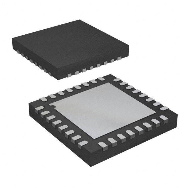
74HC4852; 74HCT4852 Nexperia 4-channel analog MUX/DEMUX with injection-current effect control DHVQFN16: plastic dual in-line compatible thermal enhanced very thin quad flat package; no leads; 16 terminals; body 2.5 x 3.5 x 0.85 mm SOT763-1 D B A A A1 E c terminal 1 detail X index area terminal 1 e1 C index area e b v M C A B y1 C y w M C 2 7 L 1 8 Eh e 16 9 15 10 Dh X 0 2.5 5 mm scale DIMENSIONS (mm are the original dimensions) A(1) UNIT max. A1 b c D(1) Dh E(1) Eh e e1 L v w y y1 0.05 0.30 3.6 2.15 2.6 1.15 0.5 mm 1 0.2 0.5 2.5 0.1 0.05 0.05 0.1 0.00 0.18 3.4 1.85 2.4 0.85 0.3 Note 1. Plastic or metal protrusions of 0.075 mm maximum per side are not included. OUTLINE REFERENCES EUROPEAN ISSUE DATE VERSION IEC JEDEC JEITA PROJECTION 02-10-17 SOT763-1 - - - MO-241 - - - 03-01-27 Fig 17. Package outline SOT763-1 (DHVQFN16) 74HC_HCT4852_3 © Nexperia B.V. 2017. All rights reserved Product data sheet Rev. 03 — 2 September 2008 17 of 20
74HC4852; 74HCT4852 Nexperia 4-channel analog MUX/DEMUX with injection-current effect control 14. Abbreviations Table 12. Abbreviations Acronym Description CDM Charged Device Model CMOS Complementary Metal Oxide Semiconductor DUT Device Under Test ESD ElectroStatic Discharge HBM Human Body Model MM Machine Model 15. Revision history Table 13. Revision history Document ID Release date Data sheet status Change notice Supersedes 74HC_HCT4852_3 20080902 Product data sheet - 74HC4852_2 Modifications: • 74HCT4852 device added. 74HC4852_2 20070530 Product data sheet - 74HC4852_1 74HC4852_1 20070323 Product data sheet - - 74HC_HCT4852_3 © Nexperia B.V. 2017. All rights reserved Product data sheet Rev. 03 — 2 September 2008 18 of 20
74HC4852; 74HCT4852 Nexperia 4-channel analog MUX/DEMUX with injection-current effect control 16. Legal information 16.1 Data sheet status Document status[1][2] Product status[3] Definition Objective [short] data sheet Development This document contains data from the objective specification for product development. Preliminary [short] data sheet Qualification This document contains data from the preliminary specification. Product [short] data sheet Production This document contains the product specification. [1] Please consult the most recently issued document before initiating or completing a design. [2] The term ‘short data sheet’ is explained in section “Definitions”. [3] Theproductstatusofdevice(s)describedinthisdocumentmayhavechangedsincethisdocumentwaspublishedandmaydifferincaseofmultipledevices.Thelatestproductstatus information is available on the Internet at URLhttp://www.nexperia.com. 16.2 Definitions malfunction of a Nexperia product can reasonably be expected to result in personal injury, death or severe property or environmental damage. Nexperia accepts no liability for inclusion and/or use of Draft —The document is a draft version only. The content is still under Nexperia products in such equipment or applications and internal review and subject to formal approval, which may result in therefore such inclusion and/or use is at the customer’s own risk. modifications or additions. Nexperia does not give any representations or warranties as to the accuracy or completeness of Applications —Applications that are described herein for any of these informationincludedhereinandshallhavenoliabilityfortheconsequencesof products are for illustrative purposes only. Nexperia makes no use of such information. representation or warranty that such applications will be suitable for the specified use without further testing or modification. Short data sheet —A short data sheet is an extract from a full data sheet withthesameproducttypenumber(s)andtitle.Ashortdatasheetisintended Limiting values —Stress above one or more limiting values (as defined in forquickreferenceonlyandshouldnotbereliedupontocontaindetailedand theAbsoluteMaximumRatingsSystemofIEC60134)maycausepermanent full information. For detailed and full information see the relevant full data damagetothedevice.Limitingvaluesarestressratingsonlyandoperationof sheet, which is available on request via the local Nexperia sales the device at these or any other conditions above those given in the office. In case of any inconsistency or conflict with the short data sheet, the Characteristics sections of this document is not implied. Exposure to limiting full data sheet shall prevail. values for extended periods may affect device reliability. Terms and conditions of sale —Nexperia products are sold 16.3 Disclaimers subjecttothegeneraltermsandconditionsofcommercialsale,aspublished athttp://www.nexperia.com/profile/terms, including those pertaining to warranty, intellectual property rights infringement and limitation of liability, unless General —Information in this document is believed to be accurate and explicitly otherwise agreed to in writing by Nexperia. In case of reliable.However,Nexperiadoesnotgiveanyrepresentationsor any inconsistency or conflict between information in this document and such warranties,expressedorimplied,astotheaccuracyorcompletenessofsuch terms and conditions, the latter will prevail. information and shall have no liability for the consequences of use of such No offer to sell or license —Nothing in this document may be interpreted information. or construed as an offer to sell products that is open for acceptance or the Right to make changes —Nexperiareservestherighttomake grant,conveyanceorimplicationofanylicenseunderanycopyrights,patents changes to information published in this document, including without or other industrial or intellectual property rights. limitation specifications and product descriptions, at any time and without notice.Thisdocumentsupersedesandreplacesallinformationsuppliedprior to the publication hereof. 16.4 Trademarks Suitability for use —Nexperia products are not designed, Notice:Allreferencedbrands,productnames,servicenamesandtrademarks authorized or warranted to be suitable for use in medical, military, aircraft, are the property of their respective owners. space or life support equipment, nor in applications where failure or 17. Contact information For more information, please visit:http://www.nexperia.com For sales office addresses, please send an email to:salesaddresses@nexperia.com 74HC_HCT4852_3 © Nexperia B.V. 2017. All rights reserved Product data sheet Rev. 03 — 2 September 2008 19 of 20
74HC4852; 74HCT4852 Nexperia 4-channel analog MUX/DEMUX with injection-current effect control 18. Contents 1 General description. . . . . . . . . . . . . . . . . . . . . . 1 2 Features . . . . . . . . . . . . . . . . . . . . . . . . . . . . . . . 1 3 Applications. . . . . . . . . . . . . . . . . . . . . . . . . . . . 2 4 Ordering information. . . . . . . . . . . . . . . . . . . . . 2 5 Functional diagram . . . . . . . . . . . . . . . . . . . . . . 2 6 Pinning information. . . . . . . . . . . . . . . . . . . . . . 4 6.1 Pinning . . . . . . . . . . . . . . . . . . . . . . . . . . . . . . . 4 6.2 Pin description . . . . . . . . . . . . . . . . . . . . . . . . . 4 7 Functional description . . . . . . . . . . . . . . . . . . . 5 8 Limiting values. . . . . . . . . . . . . . . . . . . . . . . . . . 5 9 Recommended operating conditions. . . . . . . . 6 10 Static characteristics. . . . . . . . . . . . . . . . . . . . . 6 11 Dynamic characteristics . . . . . . . . . . . . . . . . . 10 12 Waveforms . . . . . . . . . . . . . . . . . . . . . . . . . . . . 11 13 Package outline . . . . . . . . . . . . . . . . . . . . . . . . 15 14 Abbreviations. . . . . . . . . . . . . . . . . . . . . . . . . . 18 15 Revision history. . . . . . . . . . . . . . . . . . . . . . . . 18 16 Legal information. . . . . . . . . . . . . . . . . . . . . . . 19 16.1 Data sheet status . . . . . . . . . . . . . . . . . . . . . . 19 16.2 Definitions. . . . . . . . . . . . . . . . . . . . . . . . . . . . 19 16.3 Disclaimers. . . . . . . . . . . . . . . . . . . . . . . . . . . 19 16.4 Trademarks. . . . . . . . . . . . . . . . . . . . . . . . . . . 19 17 Contact information. . . . . . . . . . . . . . . . . . . . . 19 18 Contents. . . . . . . . . . . . . . . . . . . . . . . . . . . . . . 20 © Nexperia B.V. 2017. All rights reserved For more information, please visit: http://www.nexperia.com For sales office addresses, please send an email to: salesaddresses@nexperia.com Date of release: 02 September 2008