ICGOO在线商城 > 集成电路(IC) > 接口 - 模拟开关,多路复用器,多路分解器 > 74HC4851BQ-Q100,11

 Datasheet下载
- 型号: 74HC4851BQ-Q100,11
- 制造商: NXP Semiconductors
- 库位|库存: xxxx|xxxx
- 要求:
| 数量阶梯 | 香港交货 | 国内含税 |
| +xxxx | $xxxx | ¥xxxx |
查看当月历史价格
查看今年历史价格
74HC4851BQ-Q100,11产品简介:
ICGOO电子元器件商城为您提供74HC4851BQ-Q100,11由NXP Semiconductors设计生产,在icgoo商城现货销售,并且可以通过原厂、代理商等渠道进行代购。 74HC4851BQ-Q100,11价格参考。NXP Semiconductors74HC4851BQ-Q100,11封装/规格:接口 - 模拟开关,多路复用器,多路分解器, 1 Circuit IC Switch 8:1 195 Ohm 16-DHVQFN (2.5x3.5)。您可以下载74HC4851BQ-Q100,11参考资料、Datasheet数据手册功能说明书,资料中有74HC4851BQ-Q100,11 详细功能的应用电路图电压和使用方法及教程。
Nexperia USA Inc. 生产的型号为 74HC4851BQ-Q100,11 的器件属于接口类 - 模拟开关、多路复用器和多路分解器类别。以下是该型号的应用场景:

 1. 信号切换与路由
   - 应用场景:用于音频/视频信号切换、传感器信号路由等需要动态选择输入或输出信号的场合。
   - 特点:该器件支持多路输入信号的选择和传输,适用于需要灵活信号切换的系统。

 2. 数据采集系统
   - 应用场景:在工业控制、医疗设备或环境监测中,用于多通道传感器信号的采集与处理。
   - 特点:通过多路复用功能,可以减少数据采集系统的硬件复杂度,降低设计成本。

 3. 通信接口
   - 应用场景:用于通信设备中的信号隔离与切换,例如 RS-232、RS-485 或 SPI/I2C 接口的信号管理。
   - 特点:支持低功耗和高速信号传输,适合现代通信系统的严格要求。

 4. 汽车电子
   - 应用场景:在车载信息娱乐系统、驾驶辅助系统(ADAS)或车身控制系统中,用于信号分配和切换。
   - 特点:符合汽车级标准(AEC-Q100),具有高可靠性和耐久性,适应极端工作环境。

 5. 消费电子
   - 应用场景:在电视、音响、游戏机等消费电子产品中,用于音频/视频信号的切换与处理。
   - 特点:支持低电压操作,适合便携式和低功耗设备。

 6. 测试与测量设备
   - 应用场景:用于示波器、信号发生器或多通道测量仪器中,实现信号的高效切换与管理。
   - 特点:提供高精度和低失真的信号传输性能。

 总结
74HC4851BQ-Q100,11 器件凭借其多路复用/解复用功能和出色的电气特性,广泛应用于信号切换、数据采集、通信接口、汽车电子、消费电子以及测试与测量等领域。其汽车级认证使其特别适合对可靠性要求较高的场景。
| 参数 | 数值 |
| 产品目录 | 集成电路 (IC) |
| 描述 | IC MUX/DEMUX 8CH ANLG 16DHVQFN |
| 产品分类 | |
| 品牌 | NXP Semiconductors |
| 数据手册 | |
| 产品图片 |
|
| 产品型号 | 74HC4851BQ-Q100,11 |
| rohs | 无铅 / 符合限制有害物质指令(RoHS)规范要求 |
| 产品系列 | 74HC |
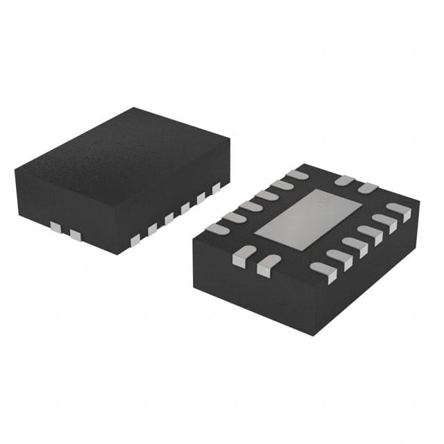
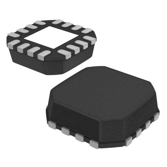
| 供应商器件封装 | 16-DHVQFN(2.5x3.5) |
| 其它名称 | 568-10130-1 |
| 功能 | 多路复用器/多路分解器 |
| 包装 | 剪切带 (CT) |
| 安装类型 | 表面贴装 |
| 导通电阻 | 195 欧姆 |
| 封装/外壳 | 16-VFQFN 裸露焊盘 |
| 工作温度 | -40°C ~ 125°C |
| 标准包装 | 1 |
| 电压-电源,单/双 (±) | 2 V ~ 6 V |
| 电压源 | 单电源 |
| 电流-电源 | 2µA |
| 电路 | 1 x 8:1 |


- 商务部:美国ITC正式对集成电路等产品启动337调查
- 曝三星4nm工艺存在良率问题 高通将骁龙8 Gen1或转产台积电
- 太阳诱电将投资9.5亿元在常州建新厂生产MLCC 预计2023年完工
- 英特尔发布欧洲新工厂建设计划 深化IDM 2.0 战略
- 台积电先进制程称霸业界 有大客户加持明年业绩稳了
- 达到5530亿美元!SIA预计今年全球半导体销售额将创下新高
- 英特尔拟将自动驾驶子公司Mobileye上市 估值或超500亿美元
- 三星加码芯片和SET,合并消费电子和移动部门,撤换高东真等 CEO
- 三星电子宣布重大人事变动 还合并消费电子和移动部门
- 海关总署:前11个月进口集成电路产品价值2.52万亿元 增长14.8%


PDF Datasheet 数据手册内容提取
74HC4851-Q100; 74HCT4851-Q100 8-channel analog multiplexer/demultiplexer with injection-current effect control Rev. 3 — 18 February 2020 Product 1. General description The 74HC4851-Q100; 74HCT4851-Q100 are high-speed Si-gate CMOS devices and are specified in compliance with JEDEC standard no. 7A. The 74HC4851-Q100; 74HCT4851-Q100 are 8-channel analog multiplexers/demultiplexers with three digital select inputs (S0 to S2), an active-LOW enable input (E), eight independent inputs/outputs (Y0 to Y7) and a common input/output (Z). The devices feature injection-current effect control, which has excellent value in automotive applications where voltages in excess of the supply voltage are common. With E LOW, one of the eight switches is selected (low impedance ON-state) by S0 to S2. With E HIGH, all switches are in the high-impedance OFF-state, independent of S0 to S2. The injection-current effect control allows signals at disabled analog input channels to exceed the supply voltage without affecting the signal of the enabled analog channel. This eliminates the need for external diode/resistor networks typically used to keep the analog channel signals within the supply-voltage range. This product has been qualified to the Automotive Electronics Council (AEC) standard Q100 (Grade 1) and is suitable for use in automotive applications. 2. Features and benefits • Automotive product qualification in accordance with AEC-Q100 (Grade 1) • Specified from -40 °C to +85 °C and from -40 °C to +125 °C • Injection-current cross coupling < 1 mV/mA • Wide supply voltage range from 2.0 V to 6.0 V for 74HC4851-Q100 • ESD protection: • MIL-STD-883, method 3015 exceeds 2000 V • HBM JESD22-A114F exceeds 2000 V • MM JESD22-A115-A exceeds 200 V (C = 200 pF, R = 0 Ω) • Latch-up performance exceeds 100 mA per JESD 78 Class II level A • Low ON-state resistance: • 400 Ω (typical) at V = 2.0 V CC • 215 Ω (typical) at V = 3.0 V CC • 120 Ω (typical) at V = 3.3 V CC • 76 Ω (typical) at V = 4.5 V CC • 59 Ω (typical) at V = 6.0 V CC • Multiple package options • DHVQFN package with Side-Wettable Flanks enabling Automatic Optical Inspection (AOI) of solder joints 3. Applications • Analog multiplexing and demultiplexing • Digital multiplexing and demultiplexing • Signal gating • Automotive application
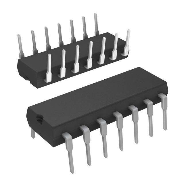
Nexperia 74HC4851-Q100; 74HCT4851-Q100 8-channel analog multiplexer/demultiplexer with injection-current effect control 4. Ordering information Table 1. Ordering information Type number Package Temperature range Name Description Version 74HC4851D-Q100 -40 °C to +125 °C SO16 plastic small outline package; 16 leads; SOT109-1 body width 3.9 mm 74HCT4851D-Q100 74HC4851PW-Q100 -40 °C to +125 °C TSSOP16 plastic thin shrink small outline package; SOT403-1 16 leads; body width 4.4 mm 74HCT4851PW-Q100 74HC4851BQ-Q100 -40 °C to +125 °C DHVQFN16 plastic dual in-line compatible thermal SOT763-1 enhanced very thin quad flat package; no leads; 74HCT4851BQ-Q100 16 terminals; body 2.5 x 3.5 x 0.85 mm 5. Functional diagram 11 0 10 0 8 X 9 7 2 6 G8 Y0 13 S0 Y1 11 14 MUX/DMUX 13 S1 Y2 0 10 15 14 1 S2 Y3 9 12 15 2 Y4 1 12 3 3 Y5 5 4 1 Y6 5 2 5 E Y7 2 6 4 6 3 4 7 Z 001aad541 001aad542 Fig. 1. Logic symbol Fig. 2. IEC logic symbol 74HC_HCT4851_Q100 All information provided in this document is subject to legal disclaimers. © Nexperia B.V. 2020. All rights reserved Product Rev. 3 — 18 February 2020 2 / 19
Nexperia 74HC4851-Q100; 74HCT4851-Q100 8-channel analog multiplexer/demultiplexer with injection-current effect control VCC 16 INJECTION 13 CURRENT Y0 CONTROL INJECTION 11 14 S0 CURRENT Y1 CONTROL INJECTION 15 CURRENT Y2 CONTROL INJECTION 10 12 S1 CURRENT Y3 CONTROL INJECTION 1-OF-8 1 CURRENT Y4 DECODER CONTROL INJECTION 9 5 S2 CURRENT Y5 CONTROL INJECTION 2 CURRENT Y6 CONTROL INJECTION 6 4 E CURRENT Y7 CONTROL INJECTION 3 CURRENT Z CONTROL 8 001aaf875 GND Fig. 3. Functional diagram 74HC_HCT4851_Q100 All information provided in this document is subject to legal disclaimers. © Nexperia B.V. 2020. All rights reserved Product Rev. 3 — 18 February 2020 3 / 19
Nexperia 74HC4851-Q100; 74HCT4851-Q100 8-channel analog multiplexer/demultiplexer with injection-current effect control 6. Pinning information 6.1. Pinning 74HC4851 74HCT4851 C terminal 1 4 C 74HC4851 index area Y V 74HCT4851 1 16 Y6 2 15 Y2 Y4 1 16 VCC Z 3 14 Y1 Y6 2 15 Y2 Y7 4 13 Y0 Y5 5 12 Y3 Z 3 14 Y1 E 6 GND(1) 11 S0 Y7 4 13 Y0 n.c. 7 10 S1 Y5 5 12 Y3 8 9 D 2 E 6 11 S0 GN S 001aaf877 n.c. 7 10 S1 Transparent top view (1) This is not a ground pin. There is no electrical or GND 8 9 S2 mechanical requirement to solder the pad. In case 001aaf876 soldered, the solder land should remain floating or connected to GND. Fig. 4. Pin configuration SOT109-1 (SO16) and SOT403-1 (TSSOP16) Fig. 5. Pin configuration SOT763-1 (DHVQFN16) 6.2. Pin description Table 2. Pin description Symbol Pin Description Y4 1 independent input/output Y6 2 independent input/output Z 3 common input/output Y7 4 independent input/output Y5 5 independent input/output E 6 enable input (active LOW) n.c. 7 not connected GND 8 ground (0 V) S2 9 select input S1 10 select input S0 11 select input Y3 12 independent input/output Y0 13 independent input/output Y1 14 independent input/output Y2 15 independent input/output V 16 supply voltage CC 74HC_HCT4851_Q100 All information provided in this document is subject to legal disclaimers. © Nexperia B.V. 2020. All rights reserved Product Rev. 3 — 18 February 2020 4 / 19
Nexperia 74HC4851-Q100; 74HCT4851-Q100 8-channel analog multiplexer/demultiplexer with injection-current effect control 7. Functional description Table 3. Function table H = HIGH voltage level; L = LOW voltage level; X = don’t care. Input Channel ON E S2 S1 S0 L L L L Y0 to Z L L L H Y1 to Z L L H L Y2 to Z L L H H Y3 to Z L H L L Y4 to Z L H L H Y5 to Z L H H L Y6 to Z L H H H Y7 to Z H X X X - 8. Limiting values Table 4. Limiting values In accordance with the Absolute Maximum Rating System (IEC 60134). Voltages are referenced to GND (ground = 0 V). Symbol Parameter Conditions Min Max Unit V supply voltage -0.5 +7.0 V CC V input voltage [1] -0.5 V + 0.5 V I CC V switch voltage [2] -0.5 V + 0.5 V SW CC I input clamping current V < -0.5 V or V > V + 0.5 V - ±20 mA IK I I CC I switch clamping current V < -0.5 V or V > V + 0.5 V - ±20 mA SK SW SW CC I switch current V > -0.5 V or V < V + 0.5 V - ±25 mA SW SW SW CC I supply current - 50 mA CC I ground current -50 - mA GND T storage temperature -65 +150 °C stg P total power dissipation T = -40 °C to +125 °C [3] - 500 mW tot amb [1] The minimum and maximum input voltage rating may be exceeded if the input clamping current rating is observed. [2] The minimum and maximum switch voltage rating may be exceeded if the switch clamping current rating is observed. [3] For SOT109-1 (SO16) package: Ptot derates linearly with 12.4 mW/K above 110 °C. For SOT403-1 (TSSOP16) package: Ptot derates linearly with 8.5 mW/K above 91 °C. For SOT763-1 (DHVQFN16) package: Ptot derates linearly with 11.2 mW/K above 106 °C. 74HC_HCT4851_Q100 All information provided in this document is subject to legal disclaimers. © Nexperia B.V. 2020. All rights reserved Product Rev. 3 — 18 February 2020 5 / 19
Nexperia 74HC4851-Q100; 74HCT4851-Q100 8-channel analog multiplexer/demultiplexer with injection-current effect control 9. Recommended operating conditions Table 5. Recommended operating conditions Symbol Parameter Conditions 74HC4851-Q100 74HCT4851-Q100 Unit Min Typ Max Min Typ Max V supply voltage 2.0 - 6.0 4.5 5.0 5.5 V CC V input voltage 0 - V 0 - V V I CC CC V switch voltage 0 - V 0 - V V SW CC CC T ambient temperature -40 - +125 -40 - +125 °C amb Δt/ΔV input transition rise and fall rate V = 2.0 V - 6.0 1000 - - - ns/V CC V = 3.0 V - 6.0 800 - - - ns/V CC V = 3.3 V - 6.0 800 - - - ns/V CC V = 4.5 V - 6.0 500 - 6.0 500 ns/V CC V = 6.0 V - 6.0 400 - - - ns/V CC 10. Static characteristics Table 6. R resistance ON At recommended operating conditions; voltages are referenced to GND (ground 0 V); For test circuit see Fig. 8. Symbol Parameter Conditions 25 °C -40 °C to -40 °C to Unit +85 °C +125 °C Min Typ Max Min Max Min Max 74HC4851-Q100 R ON resistance V = V to GND; E = V ON(peak) I CC IL (peak) V = 2.0 V; I = 2 mA - 400 650 - 670 - 700 Ω CC SW V = 3.0 V; I ≤ 2 mA - 215 330 - 360 - 380 Ω CC SW V = 3.3 V; I ≤ 2 mA - 120 270 - 305 - 345 Ω CC SW V = 4.5 V; I ≤ 2 mA - 76 210 - 240 - 270 Ω CC SW V = 6.0 V; I ≤ 2 mA - 59 195 - 220 - 250 Ω CC SW ΔR ON resistance V = 0.5 × V ; E = V ON I CC IL mismatch V = 2.0 V; I = 2 mA - 4 10 - 15 - 20 Ω CC SW between channels VCC = 3.0 V; ISW ≤ 2 mA - 2 8 - 12 - 16 Ω V = 3.3 V; I ≤ 2 mA - 2 8 - 12 - 16 Ω CC SW V = 4.5 V; I ≤ 2 mA - 2 8 - 12 - 16 Ω CC SW V = 6.0 V; I ≤ 2 mA - 3 9 - 13 - 18 Ω CC SW 74HCT4851-Q100 R ON resistance V = V to GND; E = V ON(peak) I CC IL (peak) V = 4.5 V; I ≤ 2 mA - 76 210 - 240 - 270 Ω CC SW ΔR ON resistance V = 0.5 × V ; E = V ON I CC IL mismatch V = 4.5 V; I ≤ 2 mA - 2 8 - 12 - 16 Ω CC SW between channels 74HC_HCT4851_Q100 All information provided in this document is subject to legal disclaimers. © Nexperia B.V. 2020. All rights reserved Product Rev. 3 — 18 February 2020 6 / 19
Nexperia 74HC4851-Q100; 74HCT4851-Q100 8-channel analog multiplexer/demultiplexer with injection-current effect control Table 7. Injection current coupling At recommended operating conditions; voltages are referenced to GND (ground 0 V); For test circuit see Fig. 9. Symbol Parameter Conditions 74HC4851-Q100 74HCT4851-Q100 Unit Min Typ [1] Max Min Typ [1] Max T = -40 °C to +125 °C amb ΔV output voltage |I | ≤ 1 mA; R ≤ 3.9 kΩ [2][3] O SW S variation V = 3.3 V - 0.05 1 - - - mV CC V = 5.0 V - 0.03 1 - 0.03 1 mV CC |I | ≤ 10 mA; R ≤ 3.9 kΩ SW S V = 3.3 V - 0.55 5 - - - mV CC V = 5.0 V - 0.27 5 - 0.27 5 mV CC |I | ≤ 1 mA; R ≤ 20 kΩ SW S V = 3.3 V - 0.04 2 - - - mV CC V = 5.0 V - 0.03 2 - 0.03 2 mV CC |I | ≤ 10 mA; R ≤ 20 kΩ SW S V = 3.3 V - 0.56 20 - - - mV CC V = 5.0 V - 0.48 20 - 0.48 20 mV CC [1] Typical values are measured at Tamb = 25 °C. [2] ΔVO here is the maximum variation of output voltage of an enabled analog channel when current is injected into any disabled channel. [3] ISW = total current injected into all disabled channels. Table 8. Static characteristics At recommended operating conditions; voltages are referenced to GND (ground 0 V); Symbol Parameter Conditions 25 °C -40 °C to -40 °C to Unit +85 °C +125 °C Min Typ Max Min Max Min Max 74HC4851-Q100 V HIGH-level control inputs IH input voltage V = 2.0 V 1.5 - - 1.5 - 1.5 - V CC V = 3.0 V 2.1 - - 2.1 - 2.1 - V CC V = 3.3 V 2.3 - - 2.3 - 2.3 - V CC V = 4.5 V 3.15 - - 3.15 - 3.15 - V CC V = 6.0 V 4.2 - - 4.2 - 4.2 - V CC V LOW-level control inputs IL input voltage V = 2.0 V - - 0.5 - 0.5 - 0.5 V CC V = 3.0 V - - 0.9 - 0.9 - 0.9 V CC V = 3.3 V - - 1.0 - 1.0 - 1.0 V CC V = 4.5 V - - 1.35 - 1.35 - 1.35 V CC V = 6.0 V - - 1.8 - 1.8 - 1.8 V CC 74HC_HCT4851_Q100 All information provided in this document is subject to legal disclaimers. © Nexperia B.V. 2020. All rights reserved Product Rev. 3 — 18 February 2020 7 / 19
Nexperia 74HC4851-Q100; 74HCT4851-Q100 8-channel analog multiplexer/demultiplexer with injection-current effect control Symbol Parameter Conditions 25 °C -40 °C to -40 °C to Unit +85 °C +125 °C Min Typ Max Min Max Min Max I input leakage control inputs; V = GND or V ; - - ±0.1 - ±0.1 - ±1.0 μA I I CC current V = 6.0 V CC I OFF-state E = V ; V = GND or V ; S(OFF) IH I CC leakage V = V or GND; V = 6.0 V; O CC CC current see Fig. 6 per channel - - ±0.1 - ±0.5 - ±1.0 μA all channels - - ±0.2 - ±2.0 - ±4.0 μA I ON-state E = V ; V = GND or V ; - - ±0.1 - ±0.5 - ±1.0 μA S(ON) IL I CC leakage V = V or GND; V = 6.0 V; O CC CC current see Fig. 7 I supply V = GND or V ; V = 6.0 V - - 2.0 - 5.0 - 20.0 μA CC I CC CC current C input S0, S1, S2 and E - 2 10 - 10 - 10 pF I capacitance C switch Z; OFF-state - 15 40 - 40 - 40 pF sw capacitance Yn; OFF-state - 3 15 - 15 - 15 pF 74HCT4851-Q100 V HIGH-level control inputs; 2.0 - - 2.0 - 2.0 - V IH input voltage V = 4.5 V to 5.5 V CC V LOW-level control inputs; - - 0.8 - 0.8 - 0.8 V IL input voltage V = 4.5 V to 5.5 V CC I input leakage control inputs; V = GND or V ; - - ±0.1 - ±0.1 - ±1.0 μA I I CC current V = 5.5 V CC I OFF-state E = V ; V = GND or V ; S(OFF) IH I CC leakage V = V or GND; V = 5.5 V; O CC CC current see Fig. 6 per channel - - ±0.1 - ±0.5 - ±1.0 μA all channels - - ±0.2 - ±2.0 - ±4.0 μA I ON-state E = V ; V = GND or V ; - - ±0.1 - ±0.5 - ±1.0 μA S(ON) IL I CC leakage V = V or GND; V = 5.5 V; O CC CC current see Fig. 7 I supply V = GND or V ; V = 5.5 V - - 2.0 - 5.0 - 20.0 μA CC I CC CC current ΔI additional control inputs; V = V - 2.1 V; - - 300 - 370 - 370 μA CC I CC supply other inputs at V or GND; CC current V = 4.5 V to 5.5 V; I = 0 A CC O C input S0, S1, S2 and E - 2 10 - 10 - 10 pF I capacitance C switch Z; OFF-state - 15 40 - 40 - 40 pF sw capacitance Yn; OFF-state - 3 15 - 15 - 15 pF 74HC_HCT4851_Q100 All information provided in this document is subject to legal disclaimers. © Nexperia B.V. 2020. All rights reserved Product Rev. 3 — 18 February 2020 8 / 19
Nexperia 74HC4851-Q100; 74HCT4851-Q100 8-channel analog multiplexer/demultiplexer with injection-current effect control VCC selected channel(1) Yn IS VI Z n.c. E VCC VIL E VIH Yn any disabled Yn Z channel IS IS VO GND VI GND VO 001aaf879 001aaf878 (1) Channel is selected by S0, S1 and S2. Fig. 6. Test circuit for measuring OFF-state leakage Fig. 7. Test circuit for measuring ON-state leakage current current VCC any disabled channel VI(1) Yn ISW Z VSW E V VIL VCC VI(2) Yn selected VIL E RS channel(1) GND VO Yn Z VI VI GND ISW 001aaf881 (1) Channel is selected by S0, S1 and S2. 001aaf880 VI(1) < GND or VI(1) > VCC. R = V / I . GND < V(2) < V . ON SW SW I CC Fig. 8. Test circuit for measuring ON resistance Fig. 9. Test circuit for injection current coupling 74HC_HCT4851_Q100 All information provided in this document is subject to legal disclaimers. © Nexperia B.V. 2020. All rights reserved Product Rev. 3 — 18 February 2020 9 / 19
Nexperia 74HC4851-Q100; 74HCT4851-Q100 8-channel analog multiplexer/demultiplexer with injection-current effect control 11. Dynamic characteristics Table 9. Dynamic characteristics At recommended operating conditions; voltages are referenced to GND (ground 0 V); for test circuit see Fig. 14. Symbol Parameter Conditions 25 °C -40 °C to -40 °C to Unit +85 °C +125 °C Min Typ Max Min Max Min Max 74HC4851-Q100 t propagation Z to Yn, Yn to Z; see Fig. 10 [1] pd delay V = 2.0 V - 10.0 25 - 29 - 32 ns CC V = 3.0 V - 6.0 15.5 - 17.5 - 19.5 ns CC V = 3.3 V - 5.0 14.5 - 16.5 - 18.5 ns CC V = 4.5 V - 4.0 11.5 - 12.5 - 13.5 ns CC V = 6.0 V - 3.0 10 - 11 - 12 ns CC Sn to Z, Sn to Yn; see Fig. 11 [1] V = 2.0 V - 18.0 32 - 35 - 40 ns CC V = 3.0 V - 9.5 17.5 - 20 - 23 ns CC V = 3.3 V - 8.5 16.5 - 19 - 22 ns CC V = 4.5 V - 6.5 13 - 15 - 17 ns CC V = 6.0 V - 5.0 12.5 - 14.5 - 16.5 ns CC t enable time E to Z, E to Yn; see Fig. 12 [2] en V = 2.0 V - - 95 - 105 - 115 ns CC V = 3.0 V - - 90 - 100 - 110 ns CC V = 3.3 V - - 85 - 95 - 105 ns CC V = 4.5 V - - 80 - 90 - 100 ns CC V = 6.0 V - - 78 - 80 - 80 ns CC t disable time E to Z, E to Yn; see Fig. 12 [3] dis V = 2.0 V - - 99 - 105 - 115 ns CC V = 3.0 V - - 90 - 100 - 110 ns CC V = 3.3 V - - 85 - 95 - 105 ns CC V = 4.5 V - - 80 - 90 - 100 ns CC V = 6.0 V - - 78 - 80 - 80 ns CC C power per channel; see Fig. 13 [4] PD dissipation V = 3.3 V - 28 - - - - - pF CC capacitance V = 5.0 V - 33 - - - - - pF CC 74HC_HCT4851_Q100 All information provided in this document is subject to legal disclaimers. © Nexperia B.V. 2020. All rights reserved Product Rev. 3 — 18 February 2020 10 / 19
Nexperia 74HC4851-Q100; 74HCT4851-Q100 8-channel analog multiplexer/demultiplexer with injection-current effect control Symbol Parameter Conditions 25 °C -40 °C to -40 °C to Unit +85 °C +125 °C Min Typ Max Min Max Min Max 74HCT4851-Q100 t propagation Z to Yn, Yn to Z; see Fig. 10 [1] pd delay V = 4.5 V 1.6 3.7 11.5 1.1 12.5 1.1 13.5 ns CC Sn to Z, Sn to Yn; see Fig. 11 [1] V = 4.5 V 3.2 8.0 13 2.3 15 2.3 17 ns CC t enable time E to Z, E to Yn; see Fig. 12 [2] en V = 4.5 V 4.2 8.6 25 3.0 30 3.0 35 ns CC t disable time E to Z, E to Yn; see Fig. 12 [3] dis V = 4.5 V 28.5 64.7 80 28.2 90 28 100 ns CC C power per channel; see Fig. 13 [4] PD dissipation V = 5.0 V - 30 - - - - - pF CC capacitance [1] tpd is the same as tPLH and tPHL. [2] ten is the same as tPZH and tPZL. [3] tdis is the same as tPLZ and tPHZ. [4] CPD is used to determine the dynamic power dissipation (PD in μW): PD = CPD × VCC2 × fi + ∑{(CL + Csw) × VCC2 × fo} where: fi = input frequency in MHz; fo = output frequency in MHz; ∑{(CL + Csw) × VCC2 × fo} = sum of outputs; CL = output load capacitance in pF; Csw = switch capacitance in pF; VCC = supply voltage in V. 11.1. Waveforms and test circuit VCC Z or Yn input 0.5VCC GND tPLH tPHL VCC Yn or Z 0.5VCC output GND 001aah574 Fig. 10. Input (Z, Yn) to output (Yn, Z) propagation delays VI Sn input VM GND tPLH tPHL VCC Yn or Z output VM GND 001aah575 Measurement points are given in Table 10. Fig. 11. Input (Sn) to output (Yn, Z) propagation delays 74HC_HCT4851_Q100 All information provided in this document is subject to legal disclaimers. © Nexperia B.V. 2020. All rights reserved Product Rev. 3 — 18 February 2020 11 / 19
Nexperia 74HC4851-Q100; 74HCT4851-Q100 8-channel analog multiplexer/demultiplexer with injection-current effect control VI E input VM VM 0 V tPLZ tPZL VCC Z or Yn output VM VOL VX tPHZ tPZH VOH VY Z or Yn output VM GND switch ON switch OFF switch ON 001aah576 Measurement points are given in Table 10. Logic levels: V and V are typical output voltage levels that occur with the output load. OL OH Fig. 12. Enable and disable times Table 10. Measurement points Type Input Output V V V V V M I M X Y 74HC4851-Q100 0.5V V 0.5V V + 0.1(V - V ) 0.9V CC CC CC OL CC OL OH 74HCT4851-Q100 1.3 V 3.0 V 0.5V V + 0.1(V - V ) 0.9V CC OL CC OL OH VCC A selected channel Yn G Sn Z n.c. E Yn disabled channel GND 001aah577 Fig. 13. Test circuit for measuring power dissipation capacitance 74HC_HCT4851_Q100 All information provided in this document is subject to legal disclaimers. © Nexperia B.V. 2020. All rights reserved Product Rev. 3 — 18 February 2020 12 / 19
Nexperia 74HC4851-Q100; 74HCT4851-Q100 8-channel analog multiplexer/demultiplexer with injection-current effect control switch VCC VCC open RL VI VO G tW DUT negativVeI 90 % 90 % RT CL pulse VM VM GND 10 % 0 V 001aaf883 tf tr Test data is given in Table 11. tr tf Definitions for test circuit: VI R = load resistance. 90 % L popsuitilvsee VM VM CL = load capacitance including jig and probe capacitance. 10 % 10 % 0 V R = termination resistance should be equal to the tW T 001aac221 output impedance Zo of the pulse generator. a. Input pulse definition b. Test circuit Fig. 14. Test circuit for measuring switching times Table 11. Test data Test Input Output S1 position Control E, Sn Switch Yn (Z) t, t Switch Z (Yn) r f V [1] V C R I I L L t t V V 6 ns 50 pF - open PHL, PLH CC CC t , t V V 6 ns 50 pF 10 kΩ GND PHZ PZH CC CC t , t V V 6 ns 50 pF 10 kΩ V PLZ PZL CC CC CC C V V 6 ns 0 pF - open PD CC CC [1] For 74HCT4851-Q100: input voltage VI = 3.0 V. 74HC_HCT4851_Q100 All information provided in this document is subject to legal disclaimers. © Nexperia B.V. 2020. All rights reserved Product Rev. 3 — 18 February 2020 13 / 19
Nexperia 74HC4851-Q100; 74HCT4851-Q100 8-channel analog multiplexer/demultiplexer with injection-current effect control 12. Package outline SO16: plastic small outline package; 16 leads; body width 3.9 mm SOT109-1 D E A X c y H E v M A Z 16 9 Q A 2 A 1 (A 3 ) A pin 1 index θ L p 1 8 L e w M detail X b p 0 2.5 5 mm scale DIMENSIONS (inch dimensions are derived from the original mm dimensions) UNIT mAax . A 1 A 2 A 3 b p c D (1) E (1) e H E L L p Q v w y Z (1) θ 0.25 1.45 0.49 0.25 10.0 4.0 6.2 1.0 0.7 0.7 mm 1.75 0.25 1.27 1.05 0.2 5 0.25 0.1 0.10 1.25 0.36 0.19 9.8 3.8 5.8 0.4 0.6 0.3 8 o 0.010 0.057 0.019 0.0100 0.39 0.16 0.244 0.039 0.028 0.028 0 o inches 0.069 0.01 0.05 0.041 0.01 0.01 0.004 0.004 0.049 0.014 0.0075 0.38 0.15 0.228 0.016 0.020 0.012 Note 1. Plastic or metal protrusions of 0.15 mm (0.006 inch) maximum per side are not included. OUTLINE REFERENCES EUROPEAN ISSUE DATE VERSION IEC JEDEC JEITA PROJECTION 99-12-27 SOT109-1 076E07 MS-012 03-02-19 Fig. 15. Package outline SOT109-1 (SO16) 74HC_HCT4851_Q100 All information provided in this document is subject to legal disclaimers. © Nexperia B.V. 2020. All rights reserved Product Rev. 3 — 18 February 2020 14 / 19
Nexperia 74HC4851-Q100; 74HCT4851-Q100 8-channel analog multiplexer/demultiplexer with injection-current effect control TSSOP16: plastic thin shrink small outline package; 16 leads; body width 4.4 mm SOT403-1 D E A X c y H E v M A Z 16 9 Q A 2 (A 3 ) A pin 1 index A 1 θ L p L 1 8 detail X w M e b p 0 2.5 5 mm scale DIMENSIONS (mm are the original dimensions) UNIT mAax . A 1 A 2 A 3 b p c D (1) E (2) e H E L L p Q v w y Z (1) θ 0.15 0.95 0.30 0.2 5.1 4.5 6.6 0.75 0.4 0.40 8 o mm 1.1 0.05 0.80 0.25 0.19 0.1 4.9 4.3 0.65 6.2 1 0.50 0.3 0.2 0.13 0.1 0.06 0 o Notes 1. Plastic or metal protrusions of 0.15 mm maximum per side are not included. 2. Plastic interlead protrusions of 0.25 mm maximum per side are not included. OUTLINE REFERENCES EUROPEAN ISSUE DATE VERSION IEC JEDEC JEITA PROJECTION 99-12-27 SOT403-1 MO-153 03-02-18 Fig. 16. Package outline SOT403-1 (TSSOP16) 74HC_HCT4851_Q100 All information provided in this document is subject to legal disclaimers. © Nexperia B.V. 2020. All rights reserved Product Rev. 3 — 18 February 2020 15 / 19
Nexperia 74HC4851-Q100; 74HCT4851-Q100 8-channel analog multiplexer/demultiplexer with injection-current effect control DHVQFN16: plastic dual in-line compatible thermal enhanced very thin quad flat package; no leads; 16 terminals; body 2.5 x 3.5 x 0.85 mm SOT763-1 D B A A A1 E c terminal 1 detail X index area terminal 1 e1 C index area e b v M C A B y1 C y w M C 2 7 L 1 8 Eh e 16 9 15 10 Dh X 0 2.5 5 mm scale DIMENSIONS (mm are the original dimensions) A(1) UNIT max. A1 b c D (1) Dh E (1) Eh e e1 L v w y y1 0.05 0.30 3.6 2.15 2.6 1.15 0.5 mm 1 0.2 0.5 2.5 0.1 0.05 0.05 0.1 0.00 0.18 3.4 1.85 2.4 0.85 0.3 Note 1. Plastic or metal protrusions of 0.075 mm maximum per side are not included. OUTLINE REFERENCES EUROPEAN ISSUE DATE VERSION IEC JEDEC JEITA PROJECTION 02-10-17 SOT763-1 - - - MO-241 - - - 03-01-27 Fig. 17. Package outline SOT763-1 (DHVQFN16) 74HC_HCT4851_Q100 All information provided in this document is subject to legal disclaimers. © Nexperia B.V. 2020. All rights reserved Product Rev. 3 — 18 February 2020 16 / 19
Nexperia 74HC4851-Q100; 74HCT4851-Q100 8-channel analog multiplexer/demultiplexer with injection-current effect control 13. Abbreviations Table 12. Abbreviations Acronym Description CDM Charged Device Model CMOS Complementary Metal-Oxide Semiconductor DUT Device Under Test ESD ElectroStatic Discharge HBM Human Body Model MIL Military MM Machine Model 14. Revision history Table 13. Revision history Document ID Release date Data sheet status Change notice Supersedes 74HC_HCT4851_Q100 v.3 20200218 Product data sheet - 74HC_HCT4851_Q100 v.2 Modifications: • Section 2 updated. 74HC_HCT4851_Q100 v.2 20180824 Product data sheet - 74HC_HCT4851_Q100 v.1 Modifications: • The format of this data sheet has been redesigned to comply with the identity guidelines of Nexperia. • Legal texts have been adapted to the new company name where appropriate. 74HC_HCT4851_Q100 v.1 20120802 Product data sheet - - 74HC_HCT4851_Q100 All information provided in this document is subject to legal disclaimers. © Nexperia B.V. 2020. All rights reserved Product Rev. 3 — 18 February 2020 17 / 19
Nexperia 74HC4851-Q100; 74HCT4851-Q100 8-channel analog multiplexer/demultiplexer with injection-current effect control equipment, nor in applications where failure or malfunction of an Nexperia 15. Legal information product can reasonably be expected to result in personal injury, death or severe property or environmental damage. Nexperia and its suppliers accept no liability for inclusion and/or use of Nexperia products in such equipment or applications and therefore such inclusion and/or use is at the customer's own Data sheet status risk. Quick reference data — The Quick reference data is an extract of the Document status Product Definition product data given in the Limiting values and Characteristics sections of this [1][2] status [3] document, and as such is not complete, exhaustive or legally binding. Objective [short] Development This document contains data from Applications — Applications that are described herein for any of these data sheet the objective specification for products are for illustrative purposes only. Nexperia makes no representation product development. or warranty that such applications will be suitable for the specified use without further testing or modification. Preliminary [short] Qualification This document contains data from Customers are responsible for the design and operation of their applications data sheet the preliminary specification. and products using Nexperia products, and Nexperia accepts no liability for Product [short] Production This document contains the product any assistance with applications or customer product design. It is customer’s data sheet specification. sole responsibility to determine whether the Nexperia product is suitable and fit for the customer’s applications and products planned, as well as for the planned application and use of customer’s third party customer(s). [1] Please consult the most recently issued document before initiating or Customers should provide appropriate design and operating safeguards to completing a design. minimize the risks associated with their applications and products. [2] The term 'short data sheet' is explained in section "Definitions". [3] The product status of device(s) described in this document may have Nexperia does not accept any liability related to any default, damage, costs changed since this document was published and may differ in case of or problem which is based on any weakness or default in the customer’s multiple devices. The latest product status information is available on applications or products, or the application or use by customer’s third party the internet at https://www.nexperia.com. customer(s). Customer is responsible for doing all necessary testing for the customer’s applications and products using Nexperia products in order to avoid a default of the applications and the products or of the application or Definitions use by customer’s third party customer(s). Nexperia does not accept any liability in this respect. Draft — The document is a draft version only. The content is still under internal review and subject to formal approval, which may result in Limiting values — Stress above one or more limiting values (as defined in modifications or additions. Nexperia does not give any representations or the Absolute Maximum Ratings System of IEC 60134) will cause permanent warranties as to the accuracy or completeness of information included herein damage to the device. Limiting values are stress ratings only and (proper) and shall have no liability for the consequences of use of such information. operation of the device at these or any other conditions above those given in the Recommended operating conditions section (if present) or the Short data sheet — A short data sheet is an extract from a full data sheet Characteristics sections of this document is not warranted. Constant or with the same product type number(s) and title. A short data sheet is repeated exposure to limiting values will permanently and irreversibly affect intended for quick reference only and should not be relied upon to contain the quality and reliability of the device. detailed and full information. For detailed and full information see the relevant full data sheet, which is available on request via the local Nexperia sales Terms and conditions of commercial sale — Nexperia products are office. In case of any inconsistency or conflict with the short data sheet, the sold subject to the general terms and conditions of commercial sale, as full data sheet shall prevail. published at http://www.nexperia.com/profile/terms, unless otherwise agreed in a valid written individual agreement. In case an individual agreement is Product specification — The information and data provided in a Product concluded only the terms and conditions of the respective agreement shall data sheet shall define the specification of the product as agreed between apply. Nexperia hereby expressly objects to applying the customer’s general Nexperia and its customer, unless Nexperia and customer have explicitly terms and conditions with regard to the purchase of Nexperia products by agreed otherwise in writing. In no event however, shall an agreement be customer. valid in which the Nexperia product is deemed to offer functions and qualities beyond those described in the Product data sheet. No offer to sell or license — Nothing in this document may be interpreted or construed as an offer to sell products that is open for acceptance or the grant, conveyance or implication of any license under any copyrights, patents Disclaimers or other industrial or intellectual property rights. Limited warranty and liability — Information in this document is believed Export control — This document as well as the item(s) described herein to be accurate and reliable. However, Nexperia does not give any may be subject to export control regulations. Export might require a prior representations or warranties, expressed or implied, as to the accuracy authorization from competent authorities. or completeness of such information and shall have no liability for the Translations — A non-English (translated) version of a document is for consequences of use of such information. Nexperia takes no responsibility reference only. The English version shall prevail in case of any discrepancy for the content in this document if provided by an information source outside between the translated and English versions. of Nexperia. In no event shall Nexperia be liable for any indirect, incidental, punitive, special or consequential damages (including - without limitation - lost Trademarks profits, lost savings, business interruption, costs related to the removal Notice: All referenced brands, product names, service names and or replacement of any products or rework charges) whether or not such trademarks are the property of their respective owners. damages are based on tort (including negligence), warranty, breach of contract or any other legal theory. Notwithstanding any damages that customer might incur for any reason whatsoever, Nexperia’s aggregate and cumulative liability towards customer for the products described herein shall be limited in accordance with the Terms and conditions of commercial sale of Nexperia. Right to make changes — Nexperia reserves the right to make changes to information published in this document, including without limitation specifications and product descriptions, at any time and without notice. This document supersedes and replaces all information supplied prior to the publication hereof. Suitability for use in automotive applications — This Nexperia product has been qualified for use in automotive applications. Unless otherwise agreed in writing, the product is not designed, authorized or warranted to be suitable for use in life support, life-critical or safety-critical systems or 74HC_HCT4851_Q100 All information provided in this document is subject to legal disclaimers. © Nexperia B.V. 2020. All rights reserved Product Rev. 3 — 18 February 2020 18 / 19
Nexperia 74HC4851-Q100; 74HCT4851-Q100 8-channel analog multiplexer/demultiplexer with injection-current effect control Contents 1. General description......................................................1 2. Features and benefits..................................................1 3. Applications..................................................................1 4. Ordering information....................................................2 5. Functional diagram.......................................................2 6. Pinning information......................................................4 6.1. Pinning.........................................................................4 6.2. Pin description.............................................................4 7. Functional description.................................................5 8. Limiting values.............................................................5 9. Recommended operating conditions..........................6 10. Static characteristics..................................................6 11. Dynamic characteristics...........................................10 11.1. Waveforms and test circuit.......................................11 12. Package outline........................................................14 13. Abbreviations............................................................17 14. Revision history........................................................17 15. Legal information......................................................18 © Nexperia B.V. 2020. All rights reserved For more information, please visit: http://www.nexperia.com For sales office addresses, please send an email to: salesaddresses@nexperia.com Date of release: 18 February 2020 74HC_HCT4851_Q100 All information provided in this document is subject to legal disclaimers. © Nexperia B.V. 2020. All rights reserved Product Rev. 3 — 18 February 2020 19 / 19