ICGOO在线商城 > 集成电路(IC) > PMIC - 显示器驱动器 > 74HC4511D,653
 Datasheet下载
- 型号: 74HC4511D,653
- 制造商: NXP Semiconductors
- 库位|库存: xxxx|xxxx
- 要求:
| 数量阶梯 | 香港交货 | 国内含税 |
| +xxxx | $xxxx | ¥xxxx |
查看当月历史价格
查看今年历史价格
74HC4511D,653产品简介:
ICGOO电子元器件商城为您提供74HC4511D,653由NXP Semiconductors设计生产,在icgoo商城现货销售,并且可以通过原厂、代理商等渠道进行代购。 74HC4511D,653价格参考。NXP Semiconductors74HC4511D,653封装/规格:PMIC - 显示器驱动器, 。您可以下载74HC4511D,653参考资料、Datasheet数据手册功能说明书,资料中有74HC4511D,653 详细功能的应用电路图电压和使用方法及教程。
74HC4511D,653 是由 Nexperia USA Inc. 生产的一款高速 CMOS 逻辑集成电路,属于 PMIC(电源管理集成电路)中的显示器驱动器类别。它主要用于驱动七段数码管显示器,适用于各种需要数字显示的电子设备和系统中。

该器件具有 BCD(二进制编码十进制)输入接口,可将四位二进制信号转换为对应的七段显示输出,常用于计数器、时钟、仪表盘等数字显示控制应用。其应用场景包括但不限于:

1. 消费电子产品:如电子钟、计时器、收音机频率显示等;
2. 工业控制系统:用于各类仪器仪表中的数值显示;
3. 汽车电子:车载仪表、行车记录仪、倒车雷达显示等;
4. 教育与实验设备:在教学实验箱或开发板中用于数字电路教学演示;
5. 家用电器:微波炉、洗衣机、电饭煲等带有数码显示的家电产品。

由于其高抗干扰能力、宽工作电压范围以及低功耗特性,74HC4511D 在多种嵌入式系统和数字电路设计中被广泛采用。
| 参数 | 数值 |
| 产品目录 | 集成电路 (IC)半导体 |
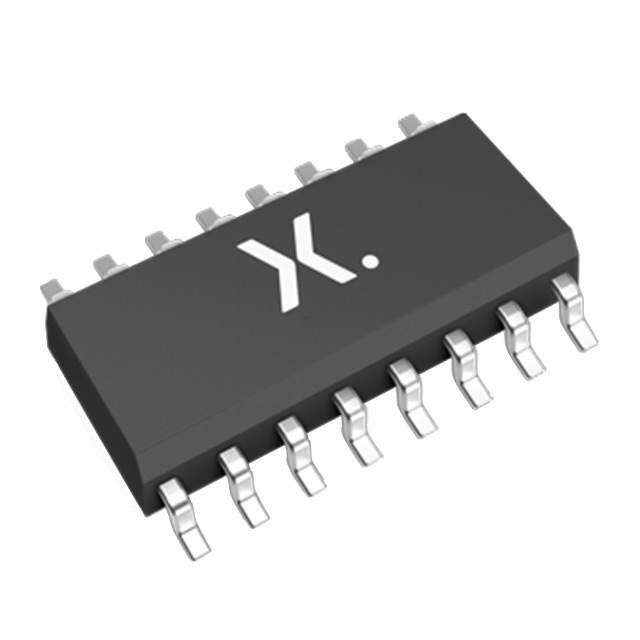
| 描述 | IC LATCH/DECODER/DRIVER 16SOIC编码器、解码器、复用器和解复用器 BCD TO 7 SEG LATCH DECODR/DEVR |
| 产品分类 | |
| 品牌 | NXP Semiconductors |
| 产品手册 | |
| 产品图片 |
|
| rohs | 符合RoHS无铅 / 符合限制有害物质指令(RoHS)规范要求 |
| 产品系列 | 逻辑集成电路,编码器、解码器、复用器和解复用器,NXP Semiconductors 74HC4511D,65374HC |
| 数据手册 | |
| 产品型号 | 74HC4511D,653 |
| PCN封装 | |
| PCN组件/产地 | |
| 产品 | Latches / Decoders / Drivers |
| 产品种类 | 编码器、解码器、复用器和解复用器 |
| 传播延迟时间 | 50 ns |
| 供应商器件封装 | 16-SO |
| 其它名称 | 568-8157-6 |
| 包装 | Digi-Reel® |
| 商标 | NXP Semiconductors |
| 安装类型 | 表面贴装 |
| 安装风格 | SMD/SMT |
| 封装 | Reel |
| 封装/外壳 | 16-SOIC(0.154",3.90mm 宽) |
| 封装/箱体 | SOT-109 |
| 工作温度 | -40°C ~ 125°C |
| 工厂包装数量 | 2500 |
| 接口 | BCD |
| 数字或字符 | - |
| 显示类型 | LED |
| 最大工作温度 | + 125 C |
| 最小工作温度 | - 40 C |
| 标准包装 | 1 |
| 电压-电源 | 2 V ~ 6 V |
| 电流-电源 | - |
| 电源电压-最大 | 6 V |
| 电源电压-最小 | 2 V |
| 输入/输出线数量 | 4 / 7 |
| 输入线路数量 | 4 |
| 输出线路数量 | 7 |
| 逻辑系列 | HC |
| 配置 | 7 段显示 |
| 零件号别名 | 74HC4511D-T |


- 商务部:美国ITC正式对集成电路等产品启动337调查
- 曝三星4nm工艺存在良率问题 高通将骁龙8 Gen1或转产台积电
- 太阳诱电将投资9.5亿元在常州建新厂生产MLCC 预计2023年完工
- 英特尔发布欧洲新工厂建设计划 深化IDM 2.0 战略
- 台积电先进制程称霸业界 有大客户加持明年业绩稳了
- 达到5530亿美元!SIA预计今年全球半导体销售额将创下新高
- 英特尔拟将自动驾驶子公司Mobileye上市 估值或超500亿美元
- 三星加码芯片和SET,合并消费电子和移动部门,撤换高东真等 CEO
- 三星电子宣布重大人事变动 还合并消费电子和移动部门
- 海关总署:前11个月进口集成电路产品价值2.52万亿元 增长14.8%


PDF Datasheet 数据手册内容提取
74HC4511; 74HCT4511 BCD to 7-segment latch/decoder/driver Rev. 3 — 15 November 2016 Product data sheet 1. General description The 74HC4511; 74HCT4511 is a BCD to 7-segment latch/decoder/driver with four address inputs (A, B, C, D), a latch enable input (LE), a ripple blanking input (BI), a lamp test input (LT), and seven segment outputs (a to g). When LE is LOW, the state of the segment outputs (a to g) is determined by the data on A to D. When LE goes HIGH, the last data present on A to D are stored in the latches and the segment outputs remain stable. When LT is LOW, all the segment outputs are HIGH independent of all other input conditions. With LT HIGH, a LOW on BI forces all segment outputs LOW. The inputs LT and BI do not affect the latch circuit. Inputs include clamp diodes. This enables the use of current limiting resistors to interface inputs to voltages in excess of V . CC 2. Features and benefits Complies with JEDEC standard no. 7A Input levels: For 74HC4511: CMOS level For 74HCT4511: TTL level Latch storage of BCD inputs Blanking input Lamp test input Driving common cathode LED displays Guaranteed 10 mA drive capability per output ESD protection: HBMJESD22-A114F exceeds 2000V MMJESD22-A115-A exceeds200V Specified from 40 C to+85C and 40C to+125C 3. Ordering information Table 1. Ordering info rmation Type number Package Temperature Name Description Version range 74HC4511D 40 C to +125 C SO16 plastic small outline package; 16leads; bodywidth3.9mm SOT109-1 74HCT4511D
74HC4511; 74HCT4511 Nexperia BCD to 7-segment latch/decoder/driver 4. Functional diagram (cid:26) (cid:20) (cid:21) (cid:25) (cid:36) (cid:37) (cid:38) (cid:39) (cid:24) (cid:47)(cid:40) (cid:47)(cid:36)(cid:55)(cid:38)(cid:43)(cid:40)(cid:54) (cid:26) (cid:36) (cid:68) (cid:20)(cid:22) (cid:23) (cid:37)(cid:44) (cid:20) (cid:37) (cid:69) (cid:20)(cid:21) (cid:39)(cid:40)(cid:38)(cid:50)(cid:39)(cid:40)(cid:53) (cid:21) (cid:38) (cid:70) (cid:20)(cid:20) (cid:25) (cid:39) (cid:71) (cid:20)(cid:19) (cid:22) (cid:47)(cid:55) (cid:39)(cid:53)(cid:44)(cid:57)(cid:40)(cid:53)(cid:54) (cid:22) (cid:47)(cid:55) (cid:72) (cid:28) (cid:23) (cid:37)(cid:44) (cid:73) (cid:20)(cid:24) (cid:74) (cid:73) (cid:72) (cid:71) (cid:70) (cid:69) (cid:68) (cid:24) (cid:47)(cid:40) (cid:74) (cid:20)(cid:23) (cid:20)(cid:23) (cid:20)(cid:24) (cid:28) (cid:20)(cid:19) (cid:20)(cid:20) (cid:20)(cid:21) (cid:20)(cid:22) (cid:68)(cid:68)(cid:68)(cid:16)(cid:19)(cid:21)(cid:23)(cid:26)(cid:25)(cid:28) (cid:68)(cid:68)(cid:68)(cid:16)(cid:19)(cid:21)(cid:23)(cid:26)(cid:26)(cid:19) Fig 1. Functional diagram Fig 2. Logic symbol (cid:37)(cid:38)(cid:39)(cid:18)(cid:26)(cid:54)(cid:40)(cid:42)(cid:3)(cid:62)(cid:55)(cid:64) (cid:22) (cid:57)(cid:20)(cid:20)(cid:62)(cid:47)(cid:55)(cid:64) (cid:23) (cid:20)(cid:22) (cid:42)(cid:20)(cid:19)(cid:62)(cid:37)(cid:44)(cid:64) (cid:68)(cid:20)(cid:19)(cid:15)(cid:20)(cid:20) (cid:20)(cid:21) (cid:69)(cid:20)(cid:19)(cid:15)(cid:20)(cid:20) (cid:24) (cid:20)(cid:20) (cid:38)(cid:28) (cid:70)(cid:20)(cid:19)(cid:15)(cid:20)(cid:20) (cid:26) (cid:20)(cid:19) (cid:28)(cid:39)(cid:15)(cid:20) (cid:71)(cid:20)(cid:19)(cid:15)(cid:20)(cid:20) (cid:20) (cid:28) (cid:28)(cid:39)(cid:15)(cid:21) (cid:72)(cid:20)(cid:19)(cid:15)(cid:20)(cid:20) (cid:21) (cid:20)(cid:24) (cid:28)(cid:39)(cid:15)(cid:23) (cid:73)(cid:20)(cid:19)(cid:15)(cid:20)(cid:20) (cid:25) (cid:20)(cid:23) (cid:28)(cid:39)(cid:15)(cid:27) (cid:74)(cid:20)(cid:19)(cid:15)(cid:20)(cid:20) (cid:68)(cid:68)(cid:68)(cid:16)(cid:19)(cid:21)(cid:23)(cid:26)(cid:26)(cid:20) Fig 3. IEC logic symbol 74HC_HCT4511 All information provided in this document is subject to legal disclaimers. © Nexperia B.V. 2017. All rights reserved Product data sheet Rev. 3 — 15 November 2016 2 of 18
74HC4511; 74HCT4511 Nexperia BCD to 7-segment latch/decoder/driver (cid:36) (cid:37) (cid:38) (cid:39) (cid:37)(cid:44) (cid:47)(cid:68)(cid:87)(cid:70)(cid:75)(cid:3)(cid:20) (cid:47)(cid:68)(cid:87)(cid:70)(cid:75)(cid:3)(cid:21) (cid:47)(cid:68)(cid:87)(cid:70)(cid:75)(cid:3)(cid:22) (cid:47)(cid:68)(cid:87)(cid:70)(cid:75)(cid:3)(cid:23) (cid:39) (cid:52) (cid:39) (cid:52) (cid:39) (cid:52) (cid:39) (cid:52) (cid:38)(cid:51) (cid:38)(cid:51) (cid:38)(cid:51) (cid:38)(cid:51) (cid:52) (cid:52) (cid:52) (cid:52) (cid:47)(cid:40) (cid:47)(cid:55) (cid:74) (cid:73) (cid:72) (cid:71) (cid:70) (cid:69) (cid:68) (cid:68)(cid:68)(cid:68)(cid:16)(cid:19)(cid:21)(cid:23)(cid:26)(cid:26)(cid:21) Fig 4. Logic diagram 74HC_HCT4511 All information provided in this document is subject to legal disclaimers. © Nexperia B.V. 2017. All rights reserved Product data sheet Rev. 3 — 15 November 2016 3 of 18
74HC4511; 74HCT4511 Nexperia BCD to 7-segment latch/decoder/driver 5. Pinning information 5.1 Pinning (cid:26)(cid:23)(cid:43)(cid:38)(cid:23)(cid:24)(cid:20)(cid:20) (cid:26)(cid:23)(cid:43)(cid:38)(cid:55)(cid:23)(cid:24)(cid:20)(cid:20) (cid:37) (cid:20) (cid:20)(cid:25) (cid:57)(cid:38)(cid:38) (cid:38) (cid:21) (cid:20)(cid:24) (cid:73) (cid:47)(cid:55) (cid:22) (cid:20)(cid:23) (cid:74) (cid:37)(cid:44) (cid:23) (cid:20)(cid:22) (cid:68) (cid:47)(cid:40) (cid:24) (cid:20)(cid:21) (cid:69) (cid:39) (cid:25) (cid:20)(cid:20) (cid:70) (cid:36) (cid:26) (cid:20)(cid:19) (cid:71) (cid:42)(cid:49)(cid:39) (cid:27) (cid:28) (cid:72) (cid:68)(cid:68)(cid:68)(cid:16)(cid:19)(cid:21)(cid:23)(cid:26)(cid:26)(cid:22) Fig 5. Pin configuration SO16 5.2 Pin description Table 2. Pin descripti on Symbol Pin Description LT 3 lamp test input (active LOW) BI 4 ripple blanking input (active low) LE 5 latch enable input (active low) A, B, C, D 7, 1, 2, 6 BCD address inputs GND 8 ground (0V) a, b, c, d, e, f, g 13, 12, 11, 10, 9, 15, 14 segments outputs V 16 supply voltage CC 74HC_HCT4511 All information provided in this document is subject to legal disclaimers. © Nexperia B.V. 2017. All rights reserved Product data sheet Rev. 3 — 15 November 2016 4 of 18
74HC4511; 74HCT4511 Nexperia BCD to 7-segment latch/decoder/driver 6. Functional description Table 3. Function tab le[1] Inputs Outputs Display LE BI LT D C B A a b c d e f g X X L X X X X H H H H H H H 8 X L H X X X X L L L L L L L blank L H H L L L L H H H H H H L 0 L H H L L L H L H H L L L L 1 L H H L L H L H H L H H L H 2 L H H L L H H H H H H L L H 3 L H H L H L L L H H L L H H 4 L H H L H L H H L H H L H H 5 L H H L H H L L L H H H H H 6 L H H L H H H H H H L L L L 7 L H H H L L L H H H H H H H 8 L H H H L L H H H H L L H H 9 L H H H L H L L L L L L L L blank L H H H L H H L L L L L L L blank L H H H H L L L L L L L L L blank L H H H H L H L L L L L L L blank L H H H H H L L L L L L L L blank L H H H H H H L L L L L L L blank H H H X X X X [2] [2] [1] H = HIGH voltage level; L = LOW voltage level; X = don’t care [2] Depends upon the BCD-code applied during the LOW-to-HIGH transition of LE. (cid:68) (cid:73) (cid:69) (cid:74) (cid:72) (cid:70) (cid:71) (cid:68)(cid:68)(cid:68)(cid:16)(cid:19)(cid:21)(cid:23)(cid:26)(cid:26)(cid:23) Fig 6. Segment designation 74HC_HCT4511 All information provided in this document is subject to legal disclaimers. © Nexperia B.V. 2017. All rights reserved Product data sheet Rev. 3 — 15 November 2016 5 of 18
74HC4511; 74HCT4511 Nexperia BCD to 7-segment latch/decoder/driver (cid:68)(cid:68)(cid:68)(cid:16)(cid:19)(cid:21)(cid:23)(cid:26)(cid:26)(cid:24) Fig 7. Display 7. Limiting values Table 4. Limiting valu es In accordance with the Absolute Maximum Rating System (IEC 60134). Voltages are referenced to GND (ground = 0 V). Symbol Parameter Conditions Min Max Unit V supply voltage 0.5 +7.0 V CC I input clamping current V < 0.5V or V >V +0.5 V - 20 mA IK I I CC I output clamping current V < 0.5 V or V > V + 0.5V - 20 mA OK O O CC I output current 0.5V <V < V +0.5V - 25 mA O O CC I supply current - +50 mA CC I ground current 50 - mA GND T storage temperature 65 +150 C stg P total power dissipation SO16 package [1] - 500 mW tot [1] For SO16 packages: above 70C the value of Ptotderates linearly at 8mW/K. 8. Recommended operating conditions Table 5. Recommend ed operating conditions Voltages are referenced to GND (ground = 0V) Symbol Parameter Conditions 74HC4511 74HCT4511 Unit Min Typ Max Min Typ Max V supply voltage 2.0 5.0 6.0 4.5 5.0 5.5 V CC V input voltage 0 - V 0 - V V I CC CC V output voltage 0 - V 0 - V V O CC CC T ambient temperature 40 +25 +125 40 +25 +125 C amb t/V input transition rise and fall rate V = 2.0 V - - 625 - - - ns/V CC V = 4.5 V - 1.67 139 - 1.67 139 ns/V CC V = 6.0 V - - 83 - - - ns/V CC 74HC_HCT4511 All information provided in this document is subject to legal disclaimers. © Nexperia B.V. 2017. All rights reserved Product data sheet Rev. 3 — 15 November 2016 6 of 18
74HC4511; 74HCT4511 Nexperia BCD to 7-segment latch/decoder/driver 9. Static characteristics Table 6. Static charac teristics At recommended operating conditions; voltages are referenced to GND (ground=0V). Symbol Parameter Conditions 25 C 40 C to +85C 40 C to +125C Unit Min Typ Max Min Max Min Max 74HC4511 V HIGH-level V =2.0V 1.5 1.2 - 1.5 - 1.5 - V IH CC input voltage V =4.5V 3.15 2.4 - 3.15 - 3.15 - V CC V =6.0V 4.2 3.2 - 4.2 - 4.2 - V CC V LOW-level V =2.0V - 0.8 0.5 - 0.5 - 0.5 V IL CC input voltage V =4.5V - 2.1 1.35 - 1.35 - 1.35 V CC V =6.0V - 2.8 1.8 - 1.8 - 1.8 V CC V HIGH-level V =V orV OH I IH IL output voltage I =7.5mA; V =4.5V 3.98 - - 3.84 - 3.7 - V O CC I =10mA; V =4.5V 3.6 - - 3.35 - 3.1 - V O CC I =7.5mA; V =6.0V 5.6 - - 5.45 - 5.35 - V O CC I =10mA; V =6.0V 5.48 - - 5.34 - 5.2 - V O CC I =15mA; V =6.0V 4.8 - - 4.5 - 4.2 - V O CC V LOW-level V =V orV OL I IH IL output voltage I =20A; V =2.0V - 0 0.1 - 0.1 - 0.1 V O CC I =20A; V =4.5V - 0 0.1 - 0.1 - 0.1 V O CC I =20A; V =6.0V - 0 0.1 - 0.1 - 0.1 V O CC I =4.0mA; V =4.5V - 0.15 0.26 - 0.33 - 0.4 V O CC I =5.2mA; V =6.0V - 0.16 0.26 - 0.33 - 0.4 V O CC I input leakage V =V orGND; - - 0.1 - 1.0 - 1.0 A I I CC current V =6.0V CC I supply current V =V orGND; I =0A; - - 8.0 - 80 - 160 A CC I CC O V =6.0V CC C input - 3.5 - - - - - pF I capacitance 74HC_HCT4511 All information provided in this document is subject to legal disclaimers. © Nexperia B.V. 2017. All rights reserved Product data sheet Rev. 3 — 15 November 2016 7 of 18
74HC4511; 74HCT4511 Nexperia BCD to 7-segment latch/decoder/driver Table 6. Static characteristics …continued At recommended operating conditions; voltages are referenced to GND (ground=0V). Symbol Parameter Conditions 25 C 40 C to +85C 40 C to +125C Unit Min Typ Max Min Max Min Max 74HCT4511 V HIGH-level V =4.5V to 5.5V 2.0 1.6 - 2.0 - 2.0 - V IH CC input voltage V LOW-level V =4.5V to 5.5V - 1.2 0.8 - 0.8 - 0.8 V IL CC input voltage V HIGH-level V =V orV ; V =4.5V OH I IH IL CC output voltage I =7.5mA 3.98 - - 3.84 - 3.7 - V O I =10mA 3.6 - - 3.35 - 3.1 - V O V LOW-level V =V orV ; V =4.5V OL I IH IL CC output voltage I =20A - 0 0.1 - 0.1 - 0.1 V O I =4.0mA - 0.15 0.26 - 0.33 - 0.4 V O I input leakage V =V orGND; - - 0.1 - 1.0 - 1.0 A I I CC current V =5.5V CC I supply current V =V orGND; - - 8.0 - 80 - 160 A CC I CC V =5.5V; I =0A CC O I additional per input pin; CC supply current V =4.5Vto5.5V; CC V =V 2.1V; I =0A; I CC O otherinputs at V orGND CC LT, LEinputs - 150 540 - 675 - 735 A BI, A, B, C, Dinputs - 30 108 - 135 - 147 A C input - 3.5 - - - - - pF I capacitance 74HC_HCT4511 All information provided in this document is subject to legal disclaimers. © Nexperia B.V. 2017. All rights reserved Product data sheet Rev. 3 — 15 November 2016 8 of 18
74HC4511; 74HCT4511 Nexperia BCD to 7-segment latch/decoder/driver 10. Dynamic characteristics Table 7. Dynamic cha racteristics Voltages are referenced to GND(ground =0V); C = 50 pF unless otherwise specified; fortestcircuitseeFigure12. L Symbol Parameter Conditions 25 C 40 C to +85 C 40 C to +125 C Unit Min Typ Max Min Max Min Max 74HC4511 t propagation A-D to a-g; see Figure8 [1] pd delay V =2.0V - 77 300 - 375 - 450 ns CC V =4.5V - 28 60 - 75 - 90 ns CC V = 5.0 V; C =15pF - 24 - - - - - ns CC L V =6.0V - 22 51 - 64 - 77 ns CC LEto a-g; see Figure9 V =2.0V - 74 270 - 330 - 405 ns CC V =4.5V - 27 54 - 68 - 81 ns CC V = 5.0 V; C =15pF - 23 - - - - - ns CC L V =6.0V - 22 46 - 58 - 69 ns CC BIto a-g; see Figure10 V =2.0V - 61 220 - 275 - 330 ns CC V =4.5V - 22 44 - 55 - 66 ns CC V = 5.0 V; C =15pF - 19 - - - - - ns CC L V =6.0V - 18 37 - 47 - 56 ns CC LTto a-g; see Figure8 V =2.0V - 41 150 - 190 - 225 ns CC V =4.5V - 15 30 - 38 - 45 ns CC V = 5.0 V; C =15pF - 12 - - - - - ns CC L V =6.0V - 12 26 - 33 - 38 ns CC t transition see Figure8, Figure9 and [2] t time Figure10 V =2.0V - 19 75 - 95 - 110 ns CC V =4.5V - 7 15 - 19 - 22 ns CC V =6.0V - 6 13 - 16 - 19 ns CC t pulse width LE LOW; seeFigure9 W V =2.0V 80 11 - 100 - 120 - ns CC V =4.5V 16 4 - 20 - 24 - ns CC V =6.0V 14 3 - 17 - 20 - ns CC t set-up time A-Dto LE; see Figure11 su V =2.0V 60 14 - 75 - 90 - ns CC V =4.5V 12 5 - 15 - 18 - ns CC V =6.0V 10 4 - 13 - 15 - ns CC 74HC_HCT4511 All information provided in this document is subject to legal disclaimers. © Nexperia B.V. 2017. All rights reserved Product data sheet Rev. 3 — 15 November 2016 9 of 18
74HC4511; 74HCT4511 Nexperia BCD to 7-segment latch/decoder/driver Table 7. Dynamic characteristics …continued Voltages are referenced to GND(ground =0V); C = 50 pF unless otherwise specified; fortestcircuitseeFigure12. L Symbol Parameter Conditions 25 C 40 C to +85 C 40 C to +125 C Unit Min Typ Max Min Max Min Max t hold time A-Dto LE; see Figure11 h V =2.0V 0 11 - 0 - 0 - ns CC V =4.5V 0 4 - 0 - 0 - ns CC V =6.0V 0 3 - 0 0 - ns CC C power V = GND to V ; V =5V; [3] - 64 - - - - - pF PD I CC CC dissipation f =1MHz i capacitance 74HCT4511 t propagation A-D to a-g; see Figure8 [1] pd delay V =4.5V - 28 60 - 75 - 90 ns CC V = 5.0 V; C =15pF - 24 - - - - - ns CC L LEto a-g; see Figure9 V =4.5V - 27 54 - 68 - 81 ns CC V = 5.0 V; C =15pF - 24 - - - - - ns CC L BIto a-g; see Figure10 V =4.5V - 23 44 - 55 - 66 ns CC V = 5.0 V; C =15pF - 20 - - - - - ns CC L LTto a-g; see Figure8 V =4.5V - 16 30 - 38 - 45 ns CC V = 5.0 V; C =15pF - 13 - - - - - ns CC L t transition see Figure8, Figure9 and [2] t time Figure10 V =4.5V - 7 15 - 19 - 22 ns CC t pulse width LE LOW; seeFigure9 W V =4.5V 16 5 - 20 - 24 - ns CC t set-up time A-Dto LE; see Figure11 su V =4.5V 12 5 - 15 - 18 - ns CC t hold time A-Dto LE; see Figure11 h V =4.5V 0 4 - 0 - 0 - ns CC C power V =GNDtoV 1.5V; [3] - 64 - - - - - pF PD I CC dissipation V =5V; f =1MHz CC i capacitance [1] t is the same as t and t . pd PHL PLH [2] t is the same as t and t . t THL TLH [3] CPD is used to determine the dynamic power dissipation (PD in W): PD=CPDVCC2fiN+(CLVCC2fo) where: f =input frequency in MHz; i f =output frequency in MHz; o C =output load capacitance in pF; L V =supply voltage in V; CC N=number of inputs switching; (CLVCC2fo)=sum of outputs. 74HC_HCT4511 All information provided in this document is subject to legal disclaimers. © Nexperia B.V. 2017. All rights reserved Product data sheet Rev. 3 — 15 November 2016 10 of 18
74HC4511; 74HCT4511 Nexperia BCD to 7-segment latch/decoder/driver 11. Waveforms (cid:20)(cid:18)(cid:73)(cid:80)(cid:68)(cid:91) (cid:57)(cid:44) (cid:57)(cid:44) (cid:47)(cid:40)(cid:3)(cid:76)(cid:81)(cid:83)(cid:88)(cid:87) (cid:57)(cid:48) (cid:36)(cid:16)(cid:39)(cid:15)(cid:3)(cid:47)(cid:55)(cid:3)(cid:76)(cid:81)(cid:83)(cid:88)(cid:87) (cid:57)(cid:48) (cid:42)(cid:49)(cid:39) (cid:42)(cid:49)(cid:39) (cid:87)(cid:58) (cid:87)(cid:51)(cid:43)(cid:47) (cid:87)(cid:51)(cid:47)(cid:43) (cid:87)(cid:51)(cid:43)(cid:47) (cid:87)(cid:51)(cid:47)(cid:43) (cid:57)(cid:50)(cid:43) (cid:28)(cid:19)(cid:3)(cid:8) (cid:28)(cid:19)(cid:3)(cid:8)(cid:3) (cid:57)(cid:50)(cid:43) (cid:28)(cid:19)(cid:3)(cid:8) (cid:28)(cid:19)(cid:3)(cid:8) (cid:68)(cid:16)(cid:74)(cid:3)(cid:82)(cid:88)(cid:87)(cid:83)(cid:88)(cid:87) (cid:57)(cid:48) (cid:57)(cid:48) (cid:68)(cid:16)(cid:74)(cid:3)(cid:82)(cid:88)(cid:87)(cid:83)(cid:88)(cid:87) (cid:20)(cid:19)(cid:3)(cid:8)(cid:3) (cid:20)(cid:19)(cid:3)(cid:8) (cid:20)(cid:19)(cid:3)(cid:8) (cid:20)(cid:19)(cid:3)(cid:8) (cid:57)(cid:50)(cid:47) (cid:57)(cid:50)(cid:47) (cid:87)(cid:55)(cid:43)(cid:47) (cid:87)(cid:55)(cid:47)(cid:43) (cid:87)(cid:55)(cid:43)(cid:47) (cid:87)(cid:55)(cid:47)(cid:43) (cid:68)(cid:68)(cid:68)(cid:16)(cid:19)(cid:21)(cid:23)(cid:26)(cid:26)(cid:25) (cid:68)(cid:68)(cid:68)(cid:16)(cid:19)(cid:21)(cid:23)(cid:26)(cid:26)(cid:26) Measurement points are given in Table8. Measurement points are given in Table8. Logic levels VOL and VOH are typical output voltage Logic levels VOL and VOH are typical output voltage levels that occur with the output load. levels that occur with the output load. Fig 8. Waveforms showing the input (A-D, LT) to Fig 9. Waveforms showing the input (LE) to output output (a-g) propagation delays and the output (a-g) propagation delays; the latch enable transition times pulse width and the output transition times (cid:57)(cid:44) (cid:37)(cid:44)(cid:3)(cid:76)(cid:81)(cid:83)(cid:88)(cid:87) (cid:57)(cid:48) (cid:57)(cid:44) (cid:42)(cid:49)(cid:39) (cid:36)(cid:16)(cid:39)(cid:3)(cid:76)(cid:81)(cid:83)(cid:88)(cid:87) (cid:57)(cid:48) (cid:87)(cid:51)(cid:43)(cid:47) (cid:87)(cid:51)(cid:47)(cid:43) (cid:42)(cid:49)(cid:39) (cid:57)(cid:50)(cid:43) (cid:87)(cid:86)(cid:88) (cid:87)(cid:86)(cid:88) (cid:28)(cid:19)(cid:3)(cid:8) (cid:28)(cid:19)(cid:3)(cid:8)(cid:3) (cid:87)(cid:75) (cid:87)(cid:75) (cid:68)(cid:16)(cid:74)(cid:3)(cid:82)(cid:88)(cid:87)(cid:83)(cid:88)(cid:87) (cid:57)(cid:48) (cid:57)(cid:44) (cid:20)(cid:19)(cid:3)(cid:8) (cid:20)(cid:19)(cid:3)(cid:8) (cid:57)(cid:50)(cid:47) (cid:47)(cid:40)(cid:3)(cid:76)(cid:81)(cid:83)(cid:88)(cid:87) (cid:57)(cid:48) (cid:87)(cid:55)(cid:43)(cid:47) (cid:87)(cid:55)(cid:47)(cid:43) (cid:42)(cid:49)(cid:39) (cid:68)(cid:68)(cid:68)(cid:16)(cid:19)(cid:21)(cid:23)(cid:26)(cid:26)(cid:27) (cid:68)(cid:68)(cid:68)(cid:16)(cid:19)(cid:21)(cid:23)(cid:26)(cid:26)(cid:28) Measurement points are given in Table8. Measurement points are given in Table8. Logic levels VOL and VOH are typical output voltage The shaded areas indicate when the input is permitted to levels that occur with the output load. change for predictable output performance. Fig 10. Waveforms showing the input (BI) to output Fig 11. Waveforms showing the data set-up and hold (a-g) propagation delays and the output times for a-g input to LE input transition times Table 8. Measuremen t points Type Input Output V V V M I M 74HC4511 0.5V GND to V 0.5V CC CC CC 74HCT4511 1.3V GND to 3V 1.3V 74HC_HCT4511 All information provided in this document is subject to legal disclaimers. © Nexperia B.V. 2017. All rights reserved Product data sheet Rev. 3 — 15 November 2016 11 of 18
74HC4511; 74HCT4511 Nexperia BCD to 7-segment latch/decoder/driver (cid:87)(cid:58) (cid:57)(cid:44) (cid:28)(cid:19)(cid:3)(cid:8) (cid:81)(cid:72)(cid:74)(cid:68)(cid:87)(cid:76)(cid:89)(cid:72)(cid:3) (cid:83)(cid:88)(cid:79)(cid:86)(cid:72) (cid:57)(cid:48) (cid:57)(cid:48) (cid:20)(cid:19)(cid:3)(cid:8) (cid:19)(cid:3)(cid:57) (cid:87)(cid:73) (cid:87)(cid:85) (cid:87)(cid:85) (cid:87)(cid:73) (cid:57)(cid:44) (cid:28)(cid:19)(cid:3)(cid:8) (cid:83)(cid:82)(cid:86)(cid:76)(cid:87)(cid:76)(cid:89)(cid:72)(cid:3) (cid:83)(cid:88)(cid:79)(cid:86)(cid:72) (cid:57)(cid:48) (cid:57)(cid:48) (cid:20)(cid:19)(cid:3)(cid:8) (cid:19)(cid:3)(cid:57) (cid:87)(cid:58) (cid:57)(cid:38)(cid:38) (cid:57)(cid:38)(cid:38) (cid:57)(cid:44) (cid:57)(cid:50) (cid:3)(cid:53)(cid:47) (cid:54)(cid:20) (cid:42) (cid:39)(cid:56)(cid:55) (cid:82)(cid:83)(cid:72)(cid:81) (cid:53)(cid:55) (cid:38)(cid:47) (cid:19)(cid:19)(cid:20)(cid:68)(cid:68)(cid:71)(cid:28)(cid:27)(cid:22) Test data is given in Table9. Test circuit definitions: RT = Termination resistance should be equal to output impedance Zo of the pulse generator CL = Load capacitance including jig and probe capacitance RL = Load resistance. S1 = Test selection switch Fig 12. Test circuit for measuring switching times Table 9. Test data Type Input Load S1 position V t, t C R t , t I r f L L PHL PLH 74HC4511 V 6ns 15pF, 50 pF 1k open CC 74HCT4511 3V 6ns 15pF, 50 pF 1k open 74HC_HCT4511 All information provided in this document is subject to legal disclaimers. © Nexperia B.V. 2017. All rights reserved Product data sheet Rev. 3 — 15 November 2016 12 of 18
74HC4511; 74HCT4511 Nexperia BCD to 7-segment latch/decoder/driver 12. Application information (cid:57)(cid:38)(cid:38) (cid:57)(cid:38)(cid:38) (cid:26)(cid:23)(cid:43)(cid:38)(cid:23)(cid:24)(cid:20)(cid:20) (cid:20)(cid:17)(cid:26)(cid:3)(cid:57) (cid:26)(cid:23)(cid:43)(cid:38)(cid:55)(cid:23)(cid:24)(cid:20)(cid:20) (cid:70)(cid:82)(cid:80)(cid:80)(cid:82)(cid:81)(cid:3)(cid:70)(cid:68)(cid:87)(cid:75)(cid:82)(cid:71)(cid:72) (cid:82)(cid:88)(cid:87)(cid:83)(cid:88)(cid:87) (cid:47)(cid:40)(cid:39) (cid:70)(cid:82)(cid:80)(cid:80)(cid:82)(cid:81)(cid:3)(cid:68)(cid:81)(cid:82)(cid:71)(cid:72) (cid:26)(cid:23)(cid:43)(cid:38)(cid:23)(cid:24)(cid:20)(cid:20) (cid:47)(cid:40)(cid:39) (cid:26)(cid:23)(cid:43)(cid:38)(cid:55)(cid:23)(cid:24)(cid:20)(cid:20) (cid:82)(cid:88)(cid:87)(cid:83)(cid:88)(cid:87) (cid:42)(cid:49)(cid:39) (cid:20)(cid:17)(cid:26)(cid:3)(cid:57) (cid:42)(cid:49)(cid:39) (cid:68)(cid:68)(cid:68)(cid:16)(cid:19)(cid:21)(cid:23)(cid:26)(cid:27)(cid:19) (cid:68)(cid:68)(cid:68)(cid:16)(cid:19)(cid:21)(cid:23)(cid:26)(cid:27)(cid:20) Fig 13. Connection to common cathode LED display Fig 14. Connection to common anode LED display readout readout (cid:72)(cid:91)(cid:70)(cid:76)(cid:87)(cid:68)(cid:87)(cid:76)(cid:82)(cid:81) (cid:86)(cid:84)(cid:88)(cid:68)(cid:85)(cid:72)(cid:3)(cid:90)(cid:68)(cid:89)(cid:72) (cid:42)(cid:49)(cid:39)(cid:3)(cid:87)(cid:82)(cid:3)(cid:57)(cid:38)(cid:38) (cid:57)(cid:38)(cid:38) (cid:26)(cid:23)(cid:43)(cid:38)(cid:23)(cid:24)(cid:20)(cid:20) (cid:26)(cid:23)(cid:43)(cid:38)(cid:55)(cid:23)(cid:24)(cid:20)(cid:20) (cid:82)(cid:88)(cid:87)(cid:83)(cid:88)(cid:87) (cid:26)(cid:23)(cid:43)(cid:38)(cid:18)(cid:43)(cid:38)(cid:55)(cid:27)(cid:25) (cid:42)(cid:49)(cid:39) (cid:68)(cid:68)(cid:68)(cid:16)(cid:19)(cid:21)(cid:23)(cid:26)(cid:27)(cid:21) Direct DC drive is not recommended as it can shorten the life of LCD displays Fig 15. Connection to LCD display readout 74HC_HCT4511 All information provided in this document is subject to legal disclaimers. © Nexperia B.V. 2017. All rights reserved Product data sheet Rev. 3 — 15 November 2016 13 of 18
74HC4511; 74HCT4511 Nexperia BCD to 7-segment latch/decoder/driver 13. Package outline (cid:54)(cid:50)(cid:20)(cid:25)(cid:29)(cid:3)(cid:83)(cid:79)(cid:68)(cid:86)(cid:87)(cid:76)(cid:70)(cid:3)(cid:86)(cid:80)(cid:68)(cid:79)(cid:79)(cid:3)(cid:82)(cid:88)(cid:87)(cid:79)(cid:76)(cid:81)(cid:72)(cid:3)(cid:83)(cid:68)(cid:70)(cid:78)(cid:68)(cid:74)(cid:72)(cid:30)(cid:3)(cid:20)(cid:25)(cid:3)(cid:79)(cid:72)(cid:68)(cid:71)(cid:86)(cid:30)(cid:3)(cid:69)(cid:82)(cid:71)(cid:92)(cid:3)(cid:90)(cid:76)(cid:71)(cid:87)(cid:75)(cid:3)(cid:22)(cid:17)(cid:28)(cid:3)(cid:80)(cid:80)(cid:3) (cid:54)(cid:50)(cid:55)(cid:20)(cid:19)(cid:28)(cid:16)(cid:20)(cid:3) (cid:39)(cid:3) (cid:40)(cid:3) (cid:36)(cid:3) (cid:59)(cid:3) (cid:70)(cid:3) (cid:92)(cid:3) (cid:43)(cid:3)(cid:40)(cid:3) (cid:89)(cid:3)(cid:48)(cid:3) (cid:36)(cid:3) (cid:61)(cid:3) (cid:20)(cid:25)(cid:3) (cid:28)(cid:3) (cid:52)(cid:3) (cid:36)(cid:3)(cid:21)(cid:3)(cid:36)(cid:3)(cid:20)(cid:3) (cid:11)(cid:36)(cid:3)(cid:22)(cid:3)(cid:3)(cid:12)(cid:3) (cid:36)(cid:3) (cid:83)(cid:76)(cid:81)(cid:3)(cid:20)(cid:3)(cid:76)(cid:81)(cid:71)(cid:72)(cid:91)(cid:3) (cid:537)(cid:3) (cid:47)(cid:3)(cid:83)(cid:3) (cid:20)(cid:3) (cid:27)(cid:3) (cid:47)(cid:3) (cid:72)(cid:3) (cid:90)(cid:3)(cid:48)(cid:3) (cid:71)(cid:72)(cid:87)(cid:68)(cid:76)(cid:79)(cid:3)(cid:59)(cid:3) (cid:69)(cid:3)(cid:83)(cid:3) (cid:19)(cid:3) (cid:21)(cid:17)(cid:24)(cid:3) (cid:24)(cid:3)(cid:80)(cid:80)(cid:3) (cid:86)(cid:70)(cid:68)(cid:79)(cid:72)(cid:3) (cid:39)(cid:44)(cid:48)(cid:40)(cid:49)(cid:54)(cid:44)(cid:50)(cid:49)(cid:54)(cid:3)(cid:11)(cid:76)(cid:81)(cid:70)(cid:75)(cid:3)(cid:71)(cid:76)(cid:80)(cid:72)(cid:81)(cid:86)(cid:76)(cid:82)(cid:81)(cid:86)(cid:3)(cid:68)(cid:85)(cid:72)(cid:3)(cid:71)(cid:72)(cid:85)(cid:76)(cid:89)(cid:72)(cid:71)(cid:3)(cid:73)(cid:85)(cid:82)(cid:80)(cid:3)(cid:87)(cid:75)(cid:72)(cid:3)(cid:82)(cid:85)(cid:76)(cid:74)(cid:76)(cid:81)(cid:68)(cid:79)(cid:3)(cid:80)(cid:80)(cid:3)(cid:71)(cid:76)(cid:80)(cid:72)(cid:81)(cid:86)(cid:76)(cid:82)(cid:81)(cid:86)(cid:12)(cid:3) (cid:56)(cid:49)(cid:44)(cid:55)(cid:3) (cid:80)(cid:36)(cid:68)(cid:91)(cid:3)(cid:17)(cid:3) (cid:36)(cid:3)(cid:20)(cid:3) (cid:36)(cid:3)(cid:21)(cid:3) (cid:36)(cid:3)(cid:22)(cid:3) (cid:69)(cid:3)(cid:83)(cid:3) (cid:70)(cid:3) (cid:39)(cid:3)(cid:11)(cid:20)(cid:12)(cid:3) (cid:40)(cid:3)(cid:11)(cid:20)(cid:12)(cid:3) (cid:72)(cid:3) (cid:43)(cid:3)(cid:40)(cid:3) (cid:47)(cid:3) (cid:47)(cid:3)(cid:83)(cid:3) (cid:52)(cid:3) (cid:89)(cid:3) (cid:90)(cid:3) (cid:92)(cid:3) (cid:61)(cid:3)(cid:11)(cid:20)(cid:12)(cid:3) (cid:537)(cid:3) (cid:80)(cid:80)(cid:3) (cid:20)(cid:17)(cid:26)(cid:24)(cid:3) (cid:19)(cid:17)(cid:21)(cid:24)(cid:3) (cid:20)(cid:17)(cid:23)(cid:24)(cid:3) (cid:19)(cid:17)(cid:21)(cid:24)(cid:3) (cid:19)(cid:17)(cid:23)(cid:28)(cid:3) (cid:19)(cid:17)(cid:21)(cid:24)(cid:3) (cid:20)(cid:19)(cid:17)(cid:19)(cid:3) (cid:23)(cid:17)(cid:19)(cid:3) (cid:20)(cid:17)(cid:21)(cid:26)(cid:3) (cid:25)(cid:17)(cid:21)(cid:3) (cid:20)(cid:17)(cid:19)(cid:3)(cid:24)(cid:3) (cid:20)(cid:17)(cid:19)(cid:3) (cid:19)(cid:17)(cid:26)(cid:3) (cid:19)(cid:17)(cid:21)(cid:3)(cid:24)(cid:3) (cid:19)(cid:17)(cid:21)(cid:24)(cid:3) (cid:19)(cid:17)(cid:20)(cid:3) (cid:19)(cid:17)(cid:26)(cid:3) (cid:19)(cid:17)(cid:20)(cid:19)(cid:3) (cid:20)(cid:17)(cid:21)(cid:24)(cid:3) (cid:19)(cid:17)(cid:22)(cid:25)(cid:3) (cid:19)(cid:17)(cid:20)(cid:28)(cid:3) (cid:28)(cid:17)(cid:27)(cid:3) (cid:22)(cid:17)(cid:27)(cid:3) (cid:24)(cid:17)(cid:27)(cid:3) (cid:19)(cid:17)(cid:23)(cid:3) (cid:19)(cid:17)(cid:25)(cid:3) (cid:19)(cid:17)(cid:22)(cid:3) (cid:27)(cid:3)(cid:82)(cid:3) (cid:19)(cid:17)(cid:19)(cid:20)(cid:19)(cid:3) (cid:19)(cid:17)(cid:19)(cid:24)(cid:26)(cid:3) (cid:19)(cid:17)(cid:19)(cid:20)(cid:28)(cid:3)(cid:19)(cid:17)(cid:19)(cid:20)(cid:19)(cid:19)(cid:3) (cid:19)(cid:17)(cid:22)(cid:28)(cid:3) (cid:19)(cid:17)(cid:20)(cid:25)(cid:3) (cid:19)(cid:17)(cid:21)(cid:23)(cid:23)(cid:3) (cid:19)(cid:17)(cid:19)(cid:22)(cid:28)(cid:3) (cid:19)(cid:17)(cid:19)(cid:21)(cid:27)(cid:3) (cid:19)(cid:17)(cid:19)(cid:21)(cid:27)(cid:3) (cid:19)(cid:3)(cid:82)(cid:3) (cid:76)(cid:81)(cid:70)(cid:75)(cid:72)(cid:86)(cid:3) (cid:19)(cid:17)(cid:19)(cid:25)(cid:28)(cid:3) (cid:19)(cid:17)(cid:19)(cid:20)(cid:3) (cid:19)(cid:17)(cid:19)(cid:24)(cid:3) (cid:19)(cid:17)(cid:19)(cid:23)(cid:20)(cid:3) (cid:19)(cid:17)(cid:19)(cid:20)(cid:3) (cid:19)(cid:17)(cid:19)(cid:20)(cid:3) (cid:19)(cid:17)(cid:19)(cid:19)(cid:23)(cid:3) (cid:19)(cid:17)(cid:19)(cid:19)(cid:23)(cid:3) (cid:19)(cid:17)(cid:19)(cid:23)(cid:28)(cid:3) (cid:19)(cid:17)(cid:19)(cid:20)(cid:23)(cid:3)(cid:19)(cid:17)(cid:19)(cid:19)(cid:26)(cid:24)(cid:3) (cid:19)(cid:17)(cid:22)(cid:27)(cid:3) (cid:19)(cid:17)(cid:20)(cid:24)(cid:3) (cid:19)(cid:17)(cid:21)(cid:21)(cid:27)(cid:3) (cid:19)(cid:17)(cid:19)(cid:20)(cid:25)(cid:3) (cid:19)(cid:17)(cid:19)(cid:21)(cid:19)(cid:3) (cid:19)(cid:17)(cid:19)(cid:20)(cid:21)(cid:3) (cid:49)(cid:82)(cid:87)(cid:72)(cid:3) (cid:20)(cid:17)(cid:3)(cid:51)(cid:79)(cid:68)(cid:86)(cid:87)(cid:76)(cid:70)(cid:3)(cid:82)(cid:85)(cid:3)(cid:80)(cid:72)(cid:87)(cid:68)(cid:79)(cid:3)(cid:83)(cid:85)(cid:82)(cid:87)(cid:85)(cid:88)(cid:86)(cid:76)(cid:82)(cid:81)(cid:86)(cid:3)(cid:82)(cid:73)(cid:3)(cid:19)(cid:17)(cid:20)(cid:24)(cid:3)(cid:80)(cid:80)(cid:3)(cid:11)(cid:19)(cid:17)(cid:19)(cid:19)(cid:25)(cid:3)(cid:76)(cid:81)(cid:70)(cid:75)(cid:12)(cid:3)(cid:80)(cid:68)(cid:91)(cid:76)(cid:80)(cid:88)(cid:80)(cid:3)(cid:83)(cid:72)(cid:85)(cid:3)(cid:86)(cid:76)(cid:71)(cid:72)(cid:3)(cid:68)(cid:85)(cid:72)(cid:3)(cid:81)(cid:82)(cid:87)(cid:3)(cid:76)(cid:81)(cid:70)(cid:79)(cid:88)(cid:71)(cid:72)(cid:71)(cid:17)(cid:3)(cid:3) (cid:50)(cid:56)(cid:55)(cid:47)(cid:44)(cid:49)(cid:40)(cid:3) (cid:3)(cid:53)(cid:40)(cid:41)(cid:40)(cid:53)(cid:40)(cid:49)(cid:38)(cid:40)(cid:54)(cid:3) (cid:40)(cid:56)(cid:53)(cid:50)(cid:51)(cid:40)(cid:36)(cid:49)(cid:3) (cid:44)(cid:54)(cid:54)(cid:56)(cid:40)(cid:3)(cid:39)(cid:36)(cid:55)(cid:40)(cid:3) (cid:57)(cid:40)(cid:53)(cid:54)(cid:44)(cid:50)(cid:49)(cid:3) (cid:3)(cid:44)(cid:40)(cid:38)(cid:3) (cid:3)(cid:45)(cid:40)(cid:39)(cid:40)(cid:38)(cid:3) (cid:3)(cid:45)(cid:40)(cid:44)(cid:55)(cid:36)(cid:3) (cid:51)(cid:53)(cid:50)(cid:45)(cid:40)(cid:38)(cid:55)(cid:44)(cid:50)(cid:49)(cid:3) (cid:28)(cid:28)(cid:16)(cid:20)(cid:21)(cid:16)(cid:21)(cid:26)(cid:3) (cid:3)(cid:54)(cid:50)(cid:55)(cid:20)(cid:19)(cid:28)(cid:16)(cid:20)(cid:3) (cid:3)(cid:19)(cid:26)(cid:25)(cid:40)(cid:19)(cid:26)(cid:3) (cid:3)(cid:48)(cid:54)(cid:16)(cid:19)(cid:20)(cid:21)(cid:3) (cid:19)(cid:22)(cid:16)(cid:19)(cid:21)(cid:16)(cid:20)(cid:28)(cid:3) Fig 16. Package outline SOT109-1 (SO16) 74HC_HCT4511 All information provided in this document is subject to legal disclaimers. © Nexperia B.V. 2017. All rights reserved Product data sheet Rev. 3 — 15 November 2016 14 of 18
74HC4511; 74HCT4511 Nexperia BCD to 7-segment latch/decoder/driver 14. Abbreviations Table 10. Abbreviation s Acronym Description CMOS Complementary Metal-Oxide Semiconductor DUT Device Under Test ESD ElectroStatic Discharge HBM Human Body Model MM Machine Model TTL Transistor-Transistor Logic 15. Revision history T able 11. Revision history Document ID Release date Data sheet status Change notice Supersedes 74HC_HCT4511 v.3 20161115 Product data sheet - 74HC_HCT4511 v.2 Modifications: • The format of this data sheet has been redesigned to comply with the new identity guidelines of NXP Semiconductors. • Legal texts have been adapted to the new company name where appropriate. • Type numbers 74HC4511N, 74HCT4511N removed. 74HC_HCT4511 v.2 19901201 Product specification - - 74HC_HCT4511 All information provided in this document is subject to legal disclaimers. © Nexperia B.V. 2017. All rights reserved Product data sheet Rev. 3 — 15 November 2016 15 of 18
74HC4511; 74HCT4511 Nexperia BCD to 7-segment latch/decoder/driver 16. Legal information 16.1 Data sheet status Document status[1][2] Product status[3] Definition Objective [short] data sheet Development This document contains data from the objective specification for product development. Preliminary [short] data sheet Qualification This document contains data from the preliminary specification. Product [short] data sheet Production This document contains the product specification. [1] Please consult the most recently issued document before initiating or completing a design. [2] The term ‘short data sheet’ is explained in section “Definitions”. [3] The product status of device(s) described in this document may have changed since this document was published and may differ in case of multiple devices. The latest product status information is available on the Internet at URLhttp://www.nexperia.com. 16.2 Definitions Suitability for use — Nexperia products are not designed, authorized or warranted to be suitable for use in life support, life-critical or safety-critical systems or equipment, nor in applications where failure or Draft — The document is a draft version only. The content is still under malfunction of a Nexperia product can reasonably be expected internal review and subject to formal approval, which may result in to result in personal injury, death or severe property or environmental modifications or additions. Nexperia does not give any damage. Nexperia and its suppliers accept no liability for representations or warranties as to the accuracy or completeness of inclusion and/or use of Nexperia products in such equipment or information included herein and shall have no liability for the consequences of applications and therefore such inclusion and/or use is at the customer’s own use of such information. risk. Short data sheet — A short data sheet is an extract from a full data sheet Applications — Applications that are described herein for any of these with the same product type number(s) and title. A short data sheet is intended products are for illustrative purposes only. Nexperia makes no for quick reference only and should not be relied upon to contain detailed and representation or warranty that such applications will be suitable for the full information. For detailed and full information see the relevant full data specified use without further testing or modification. sheet, which is available on request via the local Nexperia sales office. In case of any inconsistency or conflict with the short data sheet, the Customers are responsible for the design and operation of their applications full data sheet shall prevail. and products using Nexperia products, and Nexperia accepts no liability for any assistance with applications or customer product Product specification — The information and data provided in a Product design. It is customer’s sole responsibility to determine whether the Nexperia data sheet shall define the specification of the product as agreed between product is suitable and fit for the customer’s applications and Nexperia and its customer, unless Nexperia and products planned, as well as for the planned application and use of customer have explicitly agreed otherwise in writing. In no event however, customer’s third party customer(s). Customers should provide appropriate shall an agreement be valid in which the Nexperia product is design and operating safeguards to minimize the risks associated with their deemed to offer functions and qualities beyond those described in the applications and products. Product data sheet. Nexperia does not accept any liability related to any default, damage, costs or problem which is based on any weakness or default in the 16.3 Disclaimers customer’s applications or products, or the application or use by customer’s third party customer(s). Customer is responsible for doing all necessary testing for the customer’s applications and products using Nexperia Limited warranty and liability — Information in this document is believed to products in order to avoid a default of the applications and be accurate and reliable. However, Nexperia does not give any the products or of the application or use by customer’s third party representations or warranties, expressed or implied, as to the accuracy or customer(s). Nexperia does not accept any liability in this respect. completeness of such information and shall have no liability for the consequences of use of such information. Nexperia takes no Limiting values — Stress above one or more limiting values (as defined in responsibility for the content in this document if provided by an information the Absolute Maximum Ratings System of IEC60134) will cause permanent source outside of Nexperia. damage to the device. Limiting values are stress ratings only and (proper) operation of the device at these or any other conditions above those given in In no event shall Nexperia be liable for any indirect, incidental, the Recommended operating conditions section (if present) or the punitive, special or consequential damages (including - without limitation - lost Characteristics sections of this document is not warranted. Constant or profits, lost savings, business interruption, costs related to the removal or repeated exposure to limiting values will permanently and irreversibly affect replacement of any products or rework charges) whether or not such the quality and reliability of the device. damages are based on tort (including negligence), warranty, breach of contract or any other legal theory. Terms and conditions of commercial sale — Nexperia products are sold subject to the general terms and conditions of commercial Notwithstanding any damages that customer might incur for any reason whatsoever, Nexperia’s aggregate and cumulative liability towards sale, as published at http://www.nexperia.com/profile/terms, unless otherwise customer for the products described herein shall be limited in accordance agreed in a valid written individual agreement. In case an individual with the Terms and conditions of commercial sale of Nexperia. agreement is concluded only the terms and conditions of the respective agreement shall apply. Nexperia hereby expressly objects to Right to make changes — Nexperia reserves the right to make applying the customer’s general terms and conditions with regard to the changes to information published in this document, including without purchase of Nexperia products by customer. limitation specifications and product descriptions, at any time and without notice. This document supersedes and replaces all information supplied prior No offer to sell or license — Nothing in this document may be interpreted or to the publication hereof. construed as an offer to sell products that is open for acceptance or the grant, conveyance or implication of any license under any copyrights, patents or other industrial or intellectual property rights. 74HC_HCT4511 All information provided in this document is subject to legal disclaimers. © Nexperia B.V. 2017. All rights reserved Product data sheet Rev. 3 — 15 November 2016 16 of 18
74HC4511; 74HCT4511 Nexperia BCD to 7-segment latch/decoder/driver Export control — This document as well as the item(s) described herein Nexperia’s specifications such use shall be solely at customer’s may be subject to export control regulations. Export might require a prior own risk, and (c) customer fully indemnifies Nexperia for any authorization from competent authorities. liability, damages or failed product claims resulting from customer design and use of the product for automotive applications beyond Nexperia’s Non-automotive qualified products — Unless this data sheet expressly standard warranty and Nexperia’s product specifications. states that this specific Nexperia product is automotive qualified, the product is not suitable for automotive use. It is neither qualified nor tested Translations — A non-English (translated) version of a document is for in accordance with automotive testing or application requirements. Nexperia reference only. The English version shall prevail in case of any discrepancy accepts no liability for inclusion and/or use of between the translated and English versions. non-automotive qualified products in automotive equipment or applications. In the event that customer uses the product for design-in and use in 16.4 Trademarks automotive applications to automotive specifications and standards, customer (a) shall use the product without Nexperia’s warranty of the Notice: All referenced brands, product names, service names and trademarks product for such automotive applications, use and specifications, and (b) are the property of their respective owners. whenever customer uses the product for automotive applications beyond 17. Contact information For more information, please visit: http://www.nexperia.com For sales office addresses, please send an email to: salesaddresses@nexperia.com 74HC_HCT4511 All information provided in this document is subject to legal disclaimers. © Nexperia B.V. 2017. All rights reserved Product data sheet Rev. 3 — 15 November 2016 17 of 18
74HC4511; 74HCT4511 Nexperia BCD to 7-segment latch/decoder/driver 18. Contents 1 General description. . . . . . . . . . . . . . . . . . . . . . 1 2 Features and benefits . . . . . . . . . . . . . . . . . . . . 1 3 Ordering information. . . . . . . . . . . . . . . . . . . . . 1 4 Functional diagram . . . . . . . . . . . . . . . . . . . . . . 2 5 Pinning information. . . . . . . . . . . . . . . . . . . . . . 4 5.1 Pinning . . . . . . . . . . . . . . . . . . . . . . . . . . . . . . . 4 5.2 Pin description . . . . . . . . . . . . . . . . . . . . . . . . . 4 6 Functional description . . . . . . . . . . . . . . . . . . . 5 7 Limiting values. . . . . . . . . . . . . . . . . . . . . . . . . . 6 8 Recommended operating conditions. . . . . . . . 6 9 Static characteristics. . . . . . . . . . . . . . . . . . . . . 7 10 Dynamic characteristics. . . . . . . . . . . . . . . . . . 9 11 Waveforms . . . . . . . . . . . . . . . . . . . . . . . . . . . . 11 12 Application information. . . . . . . . . . . . . . . . . . 13 13 Package outline. . . . . . . . . . . . . . . . . . . . . . . . 14 14 Abbreviations. . . . . . . . . . . . . . . . . . . . . . . . . . 15 15 Revision history. . . . . . . . . . . . . . . . . . . . . . . . 15 16 Legal information. . . . . . . . . . . . . . . . . . . . . . . 16 16.1 Data sheet status . . . . . . . . . . . . . . . . . . . . . . 16 16.2 Definitions. . . . . . . . . . . . . . . . . . . . . . . . . . . . 16 16.3 Disclaimers. . . . . . . . . . . . . . . . . . . . . . . . . . . 16 16.4 Trademarks. . . . . . . . . . . . . . . . . . . . . . . . . . . 17 17 Contact information. . . . . . . . . . . . . . . . . . . . . 17 18 Contents. . . . . . . . . . . . . . . . . . . . . . . . . . . . . . 18 © Nexperia B.V. 2017. All rights reserved For more information, please visit: http://www.nexperia.com For sales office addresses, please send an email to: salesaddresses@nexperia.com Date of release: 15 November 2016