 Datasheet下载
- 型号: 74HC377N,652
- 制造商: NXP Semiconductors
- 库位|库存: xxxx|xxxx
- 要求:
| 数量阶梯 | 香港交货 | 国内含税 |
| +xxxx | $xxxx | ¥xxxx |
查看当月历史价格
查看今年历史价格
74HC377N,652产品简介:
ICGOO电子元器件商城为您提供74HC377N,652由NXP Semiconductors设计生产,在icgoo商城现货销售,并且可以通过原厂、代理商等渠道进行代购。 74HC377N,652价格参考。NXP Semiconductors74HC377N,652封装/规格:逻辑 - 触发器, 。您可以下载74HC377N,652参考资料、Datasheet数据手册功能说明书,资料中有74HC377N,652 详细功能的应用电路图电压和使用方法及教程。
型号为 74HC377N,652 的芯片由 NXP USA Inc. 生产,属于 逻辑 - 触发器 类别的集成电路。该芯片基于 高速CMOS逻辑(HC系列) 技术,具有低功耗、高噪声抑制能力和较强的驱动能力,适用于多种数字电路设计场景。

 应用场景包括:

1. 数据锁存与缓冲:74HC377 是一个 带使能端的8位D型触发器,常用于并行数据的锁存和缓冲,适合在微处理器系统中暂存数据或地址信号。

2. 接口扩展:在嵌入式系统或单片机应用中,该芯片可用于扩展输出端口,提升系统对外设的控制能力。

3. 时序控制电路:由于其具有同步时钟输入和使能控制功能,适用于构建需要精确时序控制的逻辑电路,如状态机或控制信号发生器。

4. 工业控制:在PLC(可编程逻辑控制器)或自动化设备中,用于实现数据的同步传输和状态保持。

5. 通信设备:在通信模块中用于数据的同步处理与信号暂存,提高系统稳定性与抗干扰能力。

6. 教育与实验开发:因其功能明确、逻辑清晰,广泛用于电子工程教学和数字电路实验平台中,帮助学生理解触发器和时序逻辑的工作原理。

综上,74HC377N,652 在数字系统中主要用于数据同步、锁存和接口控制,广泛应用于工业控制、通信、嵌入式系统和教学实验等领域。
| 参数 | 数值 |
| 产品目录 | 集成电路 (IC)半导体 |
| 描述 | IC D-TYPE POS TRG SNGL 20DIP触发器 OCTAL D F/F POS-EDGE 3STATE W/DATA ENABLE |
| 产品分类 | |
| 品牌 | NXP Semiconductors |
| 产品手册 | |
| 产品图片 |
|
| rohs | 符合RoHS无铅 / 符合限制有害物质指令(RoHS)规范要求 |
| 产品系列 | 逻辑集成电路,触发器,NXP Semiconductors 74HC377N,65274HC |
| 数据手册 | |
| 产品型号 | 74HC377N,652 |
| PCN封装 | |
| PCN组件/产地 | |
| 不同V、最大CL时的最大传播延迟 | 27ns @ 6V, 50pF |
| 产品培训模块 | http://www.digikey.cn/PTM/IndividualPTM.page?site=cn&lang=zhs&ptm=24983 |
| 产品种类 | 触发器 |
| 传播延迟时间 | 48 ns |
| 低电平输出电流 | 5.2 mA |
| 元件数 | 1 |
| 其它名称 | 568-1441-5 |
| 功能 | 标准 |
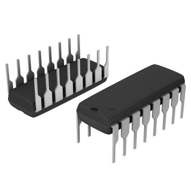
| 包装 | 管件 |
| 商标 | NXP Semiconductors |
| 安装类型 | 通孔 |
| 安装风格 | Through Hole |
| 封装 | Tube |
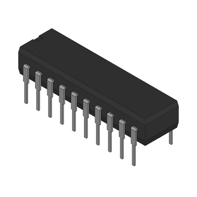
| 封装/外壳 | 20-DIP(0.300",7.62mm) |
| 封装/箱体 | DIP-20 |
| 工作温度 | -40°C ~ 125°C (TA) |
| 工厂包装数量 | 720 |
| 最大工作温度 | + 125 C |
| 最小工作温度 | - 40 C |
| 极性 | Non-Inverting |
| 标准包装 | 18 |
| 每元件位数 | 8 |
| 电压-电源 | 2 V ~ 6 V |
| 电流-输出高,低 | 5.2mA,5.2mA |
| 电流-静态 | 8µA |
| 电源电压-最大 | 6 V |
| 电源电压-最小 | 2 V |
| 电路数量 | 8 |
| 类型 | D 型 |
| 触发器类型 | 正边沿 |
| 输入电容 | 3.5pF |
| 输入类型 | Single-Ended |
| 输入线路数量 | 10 |
| 输出类型 | Single-Ended |
| 输出线路数量 | 8 |
| 逻辑类型 | D-Type Flip-Flop |
| 逻辑系列 | 74HC |
| 零件号别名 | 74HC377N |
| 频率-时钟 | 83MHz |
| 高电平输出电流 | - 5.2 mA |


- 商务部:美国ITC正式对集成电路等产品启动337调查
- 曝三星4nm工艺存在良率问题 高通将骁龙8 Gen1或转产台积电
- 太阳诱电将投资9.5亿元在常州建新厂生产MLCC 预计2023年完工
- 英特尔发布欧洲新工厂建设计划 深化IDM 2.0 战略
- 台积电先进制程称霸业界 有大客户加持明年业绩稳了
- 达到5530亿美元!SIA预计今年全球半导体销售额将创下新高
- 英特尔拟将自动驾驶子公司Mobileye上市 估值或超500亿美元
- 三星加码芯片和SET,合并消费电子和移动部门,撤换高东真等 CEO
- 三星电子宣布重大人事变动 还合并消费电子和移动部门
- 海关总署:前11个月进口集成电路产品价值2.52万亿元 增长14.8%


PDF Datasheet 数据手册内容提取
INTEGRATED CIRCUITS DATA SHEET For a complete data sheet, please also download: •The IC06 74HC/HCT/HCU/HCMOS Logic Family Specifications •The IC06 74HC/HCT/HCU/HCMOS Logic Package Information •The IC06 74HC/HCT/HCU/HCMOS Logic Package Outlines 74HC/HCT377 Octal D-type flip-flop with data enable; positive-edge trigger Product specification December 1990 File under Integrated Circuits, IC06
Philips Semiconductors Product specification Octal D-type flip-flop with data enable; 74HC/HCT377 positive-edge trigger FEATURES GENERAL DESCRIPTION • Ideal for addressable register applications The 74HC/HCT377 are high-speed Si-gate CMOS devices • Data enable for address and data synchronization and are pin compatible with low power Schottky TTL (LSTTL). They are specified in compliance with JEDEC applications standard no. 7A. • Eight positive-edge triggered D-type flip-flops • See “273” for master reset version The 74HC/HCT377 have eight edge-triggered, D-type flip-flops with individual D inputs and Q outputs. A common • See “373” for transparent latch version clock (CP) input loads all flip-flops simultaneously when • See “374” for 3-state version the data enable (E) is LOW. The state of each D input, one • Output capability: standard set-up time before the LOW-to-HIGH clock transition, is transferred to the corresponding output (Q ) of the flip-flop. • I category: MSI n CC TheEinput must be stable only one set-up time prior to the LOW-to-HIGH transition for predictable operation. QUICK REFERENCE DATA GND=0V; T =25(cid:176) C; t =t =6 ns amb r f TYPICAL SYMBOL PARAMETER CONDITIONS UNIT HC HCT t / t propagation delay CP to Q C =15pF; V =5V 13 14 ns PHL PLH n L CC f maximum clock frequency 77 53 MHz max C input capacitance 3.5 3.5 pF I C power dissipation capacitance per flip-flop notes 1 and 2 20 20 pF PD Notes 1. C is used to determine the dynamic power dissipation (P inm W): PD D P =C · V 2· f +(cid:229) (C · V 2 · f ) where: D PD CC i L CC o f =input frequency in MHz i f =output frequency in MHz o (cid:229) (C · V 2 · f )=sum of outputs L CC o C =output load capacitance in pF L V =supply voltage in V CC 2. For HC the condition is V =GND to V I CC For HCT the condition is V =GND to V - 1.5V I CC ORDERING INFORMATION See“74HC/HCT/HCU/HCMOS Logic Package Information”. December1990 2
Philips Semiconductors Product specification Octal D-type flip-flop with data enable; 74HC/HCT377 positive-edge trigger PIN DESCRIPTION PIN NO. SYMBOL NAME AND FUNCTION 1 E data enable input (active LOW) 2, 5, 6, 9, 12, 15, 16, 19 Q to Q flip-flop outputs 0 7 3, 4, 7, 8, 13, 14, 17, 18 D to D data inputs 0 7 10 GND ground (0V) 11 CP clock input (LOW-to-HIGH, edge-triggered) 20 V positive supply voltage CC Fig.1 Pin configuration. Fig.2 Logic symbol. Fig.3 IEC logic symbol. December1990 3
Philips Semiconductors Product specification Octal D-type flip-flop with data enable; 74HC/HCT377 positive-edge trigger FUNCTION TABLE INPUTS OUTPUTS OPERATING MODES CP E D Q n n load “1” › l h H load “0” › l l L hold (do nothing) › h X no change X H X no change Notes 1. H =HIGH voltage level h =HIGH voltage level one set-up time prior to the LOW-to-HIGH CP transition L =LOW voltage level I =LOW voltage level one set-up time prior to the LOW-to-HIGH CP transition › =LOW-to-HIGH CP transition X =don’t care Fig.4 Functional diagram. Fig.5 Logic diagram. December1990 4
Philips Semiconductors Product specification Octal D-type flip-flop with data enable; 74HC/HCT377 positive-edge trigger DC CHARACTERISTICS FOR 74HC For the DC characteristics see“74HC/HCT/HCU/HCMOS Logic Family Specifications”. Output capability: standard I category: MSI CC AC CHARACTERISTICS FOR 74HC GND=0V; t =t =6ns; C =50pF r f L T ((cid:176) C) TEST CONDITIONS amb 74HC SYMBOL PARAMETER UNIT WAVEFORMS V +25 - 40to+85 - 40 to+125 CC (V) min. typ. max. min. max. min. max. t / t propagation delay 44 160 200 240 ns 2.0 Fig.6 PHL PLH CP to Q 16 32 40 48 4.5 n 13 27 34 41 6.0 t / t output transition time 19 75 95 110 ns 2.0 Fig.6 THL TLH 7 15 19 22 4.5 6 13 16 19 6.0 t clock pulse width 80 14 100 120 ns 2.0 Fig.6 W HIGH or LOW 16 5 20 24 4.5 14 4 17 20 6.0 t set-up time 60 14 75 90 ns 2.0 Fig.7 su D to CP 12 5 15 18 4.5 n 10 4 13 15 6.0 t set-up time 60 6 75 90 ns 2.0 Fig.7 su E to CP 12 2 15 18 4.5 10 2 13 15 6.0 t hold time 3 - 8 3 3 ns 2.0 Fig.7 h D to CP 3 - 3 3 3 4.5 n 3 - 2 3 3 6.0 t hold time 4 - 3 4 4 ns 2.0 Fig.7 h E to CP 4 - 1 4 4 4.5 4 - 1 4 4 6.0 f maximum clock pulse 6 23 5 4 MHz 2.0 Fig.6 max frequency 30 70 24 20 4.5 35 83 28 24 6.0 December1990 5
Philips Semiconductors Product specification Octal D-type flip-flop with data enable; 74HC/HCT377 positive-edge trigger DC CHARACTERISTICS FOR 74HCT For the DC characteristics see“74HC/HCT/HCU/HCMOS Logic Family Specifications”. Output capability: standard I category: MSI CC Note to HCT types The value of additional quiescent supply current (D I ) for a unit load of 1 is given in the family specifications. CC To determineD I per input, multiply this value by the unit load coefficient shown in the table below. CC INPUT UNIT LOAD COEFFICIENT E 1.50 CP 0.50 D 0.20 n AC CHARACTERISTICS FOR 74HCT GND=0V; t =t =6ns; C =50pF r f L T ((cid:176) C) TEST CONDITIONS amb 74HCT SYMBOL PARAMETER UNIT WAVEFORMS V +25 - 40to+85 - 40 to+125 CC (V) min. typ. max. min. max. min. max. t / t propagation delay 17 32 40 48 ns 4.5 Fig.6 PHL PLH CP to Q n t / t output transition time 7 15 19 22 ns 4.5 Fig.6 THL TLH t clock pulse width 20 8 25 30 ns 4.5 Fig.6 W HIGH or LOW t set-up time 12 4 15 18 ns 4.5 Fig.7 su D to CP n t set-up time 22 12 28 33 ns 4.5 Fig.7 su E to CP t hold time 2 - 4 2 2 ns 4.5 Fig.7 h D to CP n t hold time 3 - 2 3 3 ns 4.5 Fig.7 h E to CP f maximum clock pulse 27 48 22 18 MHz 4.5 Fig.6 max frequency December1990 6
Philips Semiconductors Product specification Octal D-type flip-flop with data enable; 74HC/HCT377 positive-edge trigger AC WAVEFORMS (1) HC : VM=50%; VI=GND to VCC. HCT: VM=1.3V; VI=GND to 3V. Fig.6 Waveforms showing the clock (CP) to output (Q ) propagation delays, the clock pulse width, output n transition times and the maximum clock pulse frequency. The shaded areas indicate when the input is permitted to change for predictable output performance. (1) HC : VM=50%; VI=GND to VCC. HCT: VM=1.3V; VI=GND to 3V. Fig.7 Waveforms showing the data set-up and hold times from the data input (D ) and from the data enable input n (E) to the clock (CP). PACKAGE OUTLINES See“74HC/HCT/HCU/HCMOS Logic Package Outlines”. December1990 7