ICGOO在线商城 > 集成电路(IC) > 逻辑 - 栅极和逆变器 > 74HC1G08GW,125
 Datasheet下载
- 型号: 74HC1G08GW,125
- 制造商: NXP Semiconductors
- 库位|库存: xxxx|xxxx
- 要求:
| 数量阶梯 | 香港交货 | 国内含税 |
| +xxxx | $xxxx | ¥xxxx |
查看当月历史价格
查看今年历史价格
74HC1G08GW,125产品简介:
ICGOO电子元器件商城为您提供74HC1G08GW,125由NXP Semiconductors设计生产,在icgoo商城现货销售,并且可以通过原厂、代理商等渠道进行代购。 74HC1G08GW,125价格参考。NXP Semiconductors74HC1G08GW,125封装/规格:逻辑 - 栅极和逆变器, AND Gate IC 1 Channel 5-TSSOP。您可以下载74HC1G08GW,125参考资料、Datasheet数据手册功能说明书,资料中有74HC1G08GW,125 详细功能的应用电路图电压和使用方法及教程。
Nexperia USA Inc. 生产的74HC1G08GW,125是一款单通道AND(与)门逻辑器件,属于74HC系列。它具有低功耗、高开关速度和宽工作电压范围的特点,适用于各种数字电路设计。以下是该型号的应用场景:

 1. 消费电子设备
   在消费电子产品中,如电视、音响系统、智能家居设备等,74HC1G08GW,125可以用于信号处理和控制逻辑。例如,在音频设备中,它可以用于控制音量调节、频道选择等功能;在智能家居系统中,它可以作为传感器信号的逻辑处理单元,帮助实现自动化控制。

 2. 工业控制系统
   工业自动化系统中,74HC1G08GW,125可以用于信号的逻辑运算和控制。例如,在PLC(可编程逻辑控制器)中,它可以用于处理来自传感器的输入信号,并根据预设的逻辑条件输出控制指令,从而控制电机、阀门等执行机构的动作。

 3. 通信设备
   在通信设备中,如路由器、交换机等网络设备中,74HC1G08GW,125可以用于数据传输的逻辑控制。它可以帮助实现数据包的路由选择、流量控制等功能,确保数据的高效传输。

 4. 汽车电子
   汽车电子系统中,74HC1G08GW,125可以用于车载信息娱乐系统的控制逻辑。例如,在汽车音响系统中,它可以用于控制音频信号的切换;在车辆安全系统中,它可以用于处理传感器信号,辅助实现自动刹车、车道偏离预警等功能。

 5. 医疗设备
   医疗设备中,如心电图机、监护仪等,74HC1G08GW,125可以用于信号处理和控制逻辑。它可以帮助实现对患者生理信号的实时监测和分析,确保设备的稳定性和可靠性。

 6. 便携式设备
   在便携式设备中,如手持终端、移动电源等,74HC1G08GW,125可以用于电源管理和其他逻辑控制功能。它可以帮助优化电池使用效率,延长设备的续航时间。

 总结
74HC1G08GW,125凭借其低功耗、高可靠性和广泛的适用性,广泛应用于消费电子、工业控制、通信设备、汽车电子、医疗设备以及便携式设备等领域。它的主要作用是提供逻辑运算功能,帮助实现信号的处理和控制,确保系统的正常运行。
| 参数 | 数值 |
| 产品目录 | 集成电路 (IC)半导体 |
| 描述 | IC GATE AND 1CH 2-INP 5-TSSOP逻辑门 SINGLE 2-IN AND GATE PICOGATE |
| 产品分类 | |
| 品牌 | NXP Semiconductors |
| 产品手册 | |
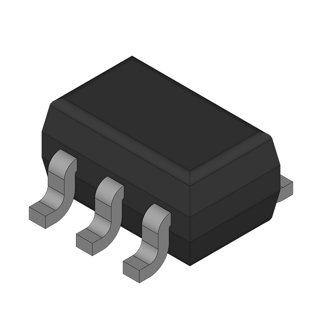
| 产品图片 |
|
| rohs | 符合RoHS无铅 / 符合限制有害物质指令(RoHS)规范要求 |
| 产品系列 | 逻辑集成电路,逻辑门,NXP Semiconductors 74HC1G08GW,12574HC |
| 数据手册 | |
| 产品型号 | 74HC1G08GW,125 |
| PCN封装 | |
| PCN组件/产地 | |
| 不同V、最大CL时的最大传播延迟 | 23ns @ 6V,50pF |
| 产品 | AND |
| 产品培训模块 | http://www.digikey.cn/PTM/IndividualPTM.page?site=cn&lang=zhs&ptm=24983 |
| 产品目录页面 | |
| 产品种类 | 逻辑门 |
| 传播延迟时间 | 27 ns |
| 低电平输出电流 | 2.6 mA |
| 供应商器件封装 | 5-TSSOP |
| 其它名称 | 568-2639-6 |
| 包装 | Digi-Reel® |
| 商标 | NXP Semiconductors |
| 安装类型 | 表面贴装 |
| 安装风格 | SMD/SMT |
| 封装 | Reel |
| 封装/外壳 | 6-TSSOP(5 引线),SC-88A,SOT-353 |
| 封装/箱体 | SOT-353 |
| 工作温度 | -40°C ~ 125°C |
| 工厂包装数量 | 3000 |
| 最大工作温度 | + 125 C |
| 最小工作温度 | - 40 C |
| 栅极数量 | 1 Gate |
| 标准包装 | 1 |
| 特性 | - |
| 电压-电源 | 2 V ~ 6 V |
| 电流-输出高,低 | 2.6mA,2.6mA |
| 电流-静态(最大值) | 20µA |
| 电源电压-最大 | 6 V |
| 电源电压-最小 | 2 V |
| 电路数 | 1 |
| 输入/输出线数量 | 2 / 1 |
| 输入数 | 2 |
| 输入线路数量 | 2 |
| 输出线路数量 | 1 |
| 逻辑电平-低 | 0.5 V ~ 1.8 V |
| 逻辑电平-高 | 1.5 V ~ 4.2 V |
| 逻辑类型 | 与门 |
| 逻辑系列 | 74HC |
| 零件号别名 | 74HC1G08GW-G |
| 高电平输出电流 | - 2.6 mA |


- 商务部:美国ITC正式对集成电路等产品启动337调查
- 曝三星4nm工艺存在良率问题 高通将骁龙8 Gen1或转产台积电
- 太阳诱电将投资9.5亿元在常州建新厂生产MLCC 预计2023年完工
- 英特尔发布欧洲新工厂建设计划 深化IDM 2.0 战略
- 台积电先进制程称霸业界 有大客户加持明年业绩稳了
- 达到5530亿美元!SIA预计今年全球半导体销售额将创下新高
- 英特尔拟将自动驾驶子公司Mobileye上市 估值或超500亿美元
- 三星加码芯片和SET,合并消费电子和移动部门,撤换高东真等 CEO
- 三星电子宣布重大人事变动 还合并消费电子和移动部门
- 海关总署:前11个月进口集成电路产品价值2.52万亿元 增长14.8%


PDF Datasheet 数据手册内容提取
74HC1G08; 74HCT1G08 2-input AND gate Rev. 5 — 14 March 2018 Product data sheet 1 General description The 74HC1G08; 74HCT1G08 is a single 2-input AND gate. Inputs include clamp diodes. This enables the use of current limiting resistors to interface inputs to voltages in excess of V . CC 2 Features • Input levels: –For 74HC1G08: CMOS level –For 74HCT1G08: TTL level • Symmetrical output impedance • High noise immunity • Low power dissipation • Balanced propagation delays • ESD protection: –HBM JESD22-A114F exceeds 2000 V –MM JESD22-A115-A exceeds 200 V • Multiple package options • Specified from −40 °C to +85 °C and −40 °C to +125 °C 3 Ordering information Table 1. Ordering information Type number Package Temperature range Name Description Version 74HC1G08GW -40 °C to +125 °C TSSOP5 plastic thin shrink small outline package; 5 leads; SOT353-1 body width 1.25 mm 74HCT1G08GW 74HC1G08GV -40 °C to +125 °C SC-74A plastic surface-mounted package; 5 leads SOT753 74HCT1G08GV
Nexperia 74HC1G08; 74HCT1G08 2-input AND gate 4 Marking Table 2. Marking codes Type number Marking 74HC1G08GW HE 74HCT1G08GW TE 74HC1G08GV H08 74HCT1G08GV T08 5 Functional diagram 1 B 1 Y 4 & 4 2 A 2 mna113 mna114 Figure 1. Logic symbol Figure 2. IEC logic symbol B Y A mna115 Figure 3. Logic diagram 6 Pinning information 6.1 Pinning 74HC1G08 74HCT1G08 B 1 5 VCC A 2 GND 3 4 Y 001aaf102 Figure 4. Pin configuration 74HC_HCT1G08 All information provided in this document is subject to legal disclaimers. © Nexperia B.V. 2018. All rights reserved. Product data sheet Rev. 5 — 14 March 2018 2 / 12
Nexperia 74HC1G08; 74HCT1G08 2-input AND gate 6.2 Pin description Table 3. Pin description Symbol Pin Description B 1 data input A 2 data input GND 3 ground (0 V) Y 4 data output V 5 supply voltage CC 7 Functional description Table 4. Function table H = HIGH voltage level; L = LOW voltage level Input Output A B Y L L L L H L H L L H H H 8 Limiting values Table 5. Limiting values [1] In accordance with the Absolute Maximum Rating System (IEC 60134). Voltages are referenced to GND (ground = 0 V). Symbol Parameter Conditions Min Max Unit V supply voltage -0.5 +7.0 V CC I input clamping current V < -0.5 V or V > V + 0.5 V - ±20 mA IK I I CC I output clamping current V < -0.5 V or V > V + 0.5 V - ±20 mA OK O O CC I output current -0.5 V < V < V + 0.5 V - ±12.5 mA O O CC I supply current - 25 mA CC I ground current -25 - mA GND T storage temperature -65 +150 °C stg [2] P total power dissipation T = -40 °C to +125 °C - 200 mW tot amb [1] The input and output voltage ratings may be exceeded if the input and output current ratings are observed. [2] Above 55 °C the value of Ptot derates linearly with 2.5 mW/K. 74HC_HCT1G08 All information provided in this document is subject to legal disclaimers. © Nexperia B.V. 2018. All rights reserved. Product data sheet Rev. 5 — 14 March 2018 3 / 12
Nexperia 74HC1G08; 74HCT1G08 2-input AND gate 9 Recommended operating conditions Table 6. Recommended operating conditions Voltages are referenced to GND (ground = 0 V). Symbol Parameter Conditions 74HC1G08 74HCT1G08 Unit Min Typ Max Min Typ Max V supply voltage 2.0 5.0 6.0 4.5 5.0 5.5 V CC V input voltage 0 - V 0 - V V I CC CC V output voltage 0 - V 0 - V V O CC CC T ambient temperature -40 +25 +125 -40 +25 +125 °C amb Δt/ΔV input transition rise V = 2.0 V - - 625 - - - ns/V CC and fall rate V = 4.5 V - - 139 - - 139 ns/V CC V = 6.0 V - - 83 - - - ns/V CC 10 Static characteristics Table 7. Static characteristics Voltages are referenced to GND (ground = 0 V). All typical values are measured at T = 25 °C. amb Symbol Parameter Conditions -40 °C to +85 °C -40 °C to +125 °C Unit Min Typ Max Min Max 74HC1G08 V HIGH-level input V = 2.0 V 1.5 1.2 - 1.5 - V IH CC voltage V = 4.5 V 3.15 2.4 - 3.15 - V CC V = 6.0 V 4.2 3.2 - 4.2 - V CC V LOW-level input V = 2.0 V - 0.8 0.5 - 0.5 V IL CC voltage V = 4.5 V - 2.1 1.35 - 1.35 V CC V = 6.0 V - 2.8 1.8 - 1.8 V CC V HIGH-level output V = V or V OH I IH IL voltage I = -20 μA; V = 2.0 V 1.9 2.0 - 1.9 - V O CC I = -20 μA; V = 4.5 V 4.4 4.5 - 4.4 - V O CC I = -20 μA; V = 6.0 V 5.9 6.0 - 5.9 - V O CC I = -2.0 mA; V = 4.5 V 4.13 4.32 - 3.7 - V O CC I = -2.6 mA; V = 6.0 V 5.63 5.81 - 5.2 - V O CC V LOW-level output V = V or V OL I IH IL voltage I = 20 μA; V = 2.0 V - 0 0.1 - 0.1 V O CC I = 20 μA; V = 4.5 V - 0 0.1 - 0.1 V O CC I = 20 μA; V = 6.0 V - 0 0.1 - 0.1 V O CC I = 2.0 mA; V = 4.5 V - 0.15 0.33 - 0.4 V O CC I = 2.6 mA; V = 6.0 V - 0.16 0.33 - 0.4 V O CC I input leakage current V = V or GND; V = 6.0 V - - 1.0 - 1.0 μA I I CC CC 74HC_HCT1G08 All information provided in this document is subject to legal disclaimers. © Nexperia B.V. 2018. All rights reserved. Product data sheet Rev. 5 — 14 March 2018 4 / 12
Nexperia 74HC1G08; 74HCT1G08 2-input AND gate Symbol Parameter Conditions -40 °C to +85 °C -40 °C to +125 °C Unit Min Typ Max Min Max I supply current V = V or GND; I = 0 A; - - 10 - 20 μA CC I CC O V = 6.0 V CC C input capacitance - 1.5 - - - pF I 74HCT1G08 V HIGH-level input V = 4.5 V to 5.5 V 2.0 1.6 - 2.0 - V IH CC voltage V LOW-level input V = 4.5 V to 5.5 V - 1.2 0.8 - 0.8 V IL CC voltage V HIGH-level output V = V or V OH I IH IL voltage I = -20 μA; V = 4.5 V 4.4 4.5 - 4.4 - V O CC I = -2.0 mA; V = 4.5 V 4.13 4.32 - 3.7 - V O CC V LOW-level output V = V or V OL I IH IL voltage I = 20 μA; V = 4.5 V - 0 0.1 - 0.1 V O CC I = 2.0 mA; V = 4.5 V - 0.15 0.33 - 0.4 V O CC I input leakage current V = V or GND; V = 5.5 V - - 1.0 - 1.0 μA I I CC CC I supply current V = V or GND; I = 0 A; - - 10 - 20 μA CC I CC O V = 5.5 V CC ΔI additional supply per input; V = 4.5 V to 5.5 V; - - 500 - 850 μA CC CC current V = V - 2.1 V; I = 0 A I CC O C input capacitance - 1.5 - - - pF I 11 Dynamic characteristics Table 8. Dynamic characteristics GND = 0 V; t = t ≤ 6.0 ns; All typical values are measured at T = 25 °C. For test circuit see Figure 6 r f amb Symbol Parameter Conditions -40 °C to +85 °C -40 °C to +125 °C Unit Min Typ Max Min Max 74HC1G08 [1] t propagation delay A and B to Y; see Figure 5 pd V = 2.0 V; C = 50 pF - 25 115 - 135 ns CC L V = 4.5 V; C = 50 pF - 9 23 - 27 ns CC L V = 5.0 V; C = 15 pF - 7 - - - ns CC L V = 6.0 V; C = 50 pF - 8 20 - 23 ns CC L [2] C power dissipation V = GND to V - 19 - - - pF PD I CC capacitance 74HC_HCT1G08 All information provided in this document is subject to legal disclaimers. © Nexperia B.V. 2018. All rights reserved. Product data sheet Rev. 5 — 14 March 2018 5 / 12
Nexperia 74HC1G08; 74HCT1G08 2-input AND gate Symbol Parameter Conditions -40 °C to +85 °C -40 °C to +125 °C Unit Min Typ Max Min Max 74HCT1G08 [1] t propagation delay A and B to Y; see Figure 5 pd V = 4.5 V; C = 50 pF - 11 23 - 27 ns CC L V = 5.0 V; C = 15 pF - 11 - - - ns CC L [2] C power dissipation V = GND to V - 1.5 V - 21 - - - pF PD I CC capacitance [1] tpd is the same as tPLH and tPHL. [2] CPD is used to determine the dynamic power dissipation PD (μW). PD = CPD x VCC2 x fi + ∑(CL x VCC2 x fo) where: fi = input frequency in MHz fo = output frequency in MHz CL = output load capacitance in pF VCC = supply voltage in Volts ∑(CL x VCC2 x fo) = sum of outputs 11.1 Waveform and test circuit VCC VI VO PULSE A,Binput VM GENERATOR DUT RT CL tPHL tPLH mna101 Test data is given in Table 8. Definitions for test Youtput VM circuit: mna116 CL = Load capacitance including jig and probe For 74HC1G08: V = 0.5 x V ; V = GND to V capacitance M CC I CC For 74HCT1G08: VM = 1.3 V; VI = GND to 3.0 V RT = Termination resistance should be equal to the output impedance Z of the pulse generator Figure 5. The input (A and B) to output (Y) propagation o delays Figure 6. Test circuit for measuring switching times 74HC_HCT1G08 All information provided in this document is subject to legal disclaimers. © Nexperia B.V. 2018. All rights reserved. Product data sheet Rev. 5 — 14 March 2018 6 / 12
Nexperia 74HC1G08; 74HCT1G08 2-input AND gate 12 Package outline TSSOP5:plasticthinshrinksmalloutlinepackage;5leads;bodywidth1.25mm SOT353-1 D E A X c y HE v M A Z 5 4 A2 A A1 (A3) θ 1 3 Lp L e w M bp e1 detailX 0 1.5 3mm scale DIMENSIONS(mmaretheoriginaldimensions) UNIT mAax. A1 A2 A3 bp c D(1) E(1) e e1 HE L Lp v w y Z(1) θ 0.1 1.0 0.30 0.25 2.25 1.35 2.25 0.46 0.60 7° mm 1.1 0.15 0.65 1.3 0.425 0.3 0.1 0.1 0 0.8 0.15 0.08 1.85 1.15 2.0 0.21 0.15 0° Note 1.Plasticormetalprotrusionsof0.15mmmaximumpersidearenotincluded. OUTLINE REFERENCES EUROPEAN ISSUEDATE VERSION IEC JEDEC JEITA PROJECTION 00-09-01 SOT353-1 MO-203 SC-88A 03-02-19 Figure 7. Package outline SOT353-1 (TSSOP5) 74HC_HCT1G08 All information provided in this document is subject to legal disclaimers. © Nexperia B.V. 2018. All rights reserved. Product data sheet Rev. 5 — 14 March 2018 7 / 12
Nexperia 74HC1G08; 74HCT1G08 2-input AND gate Plasticsurface-mountedpackage;5leads SOT753 D B E A X y HE v M A 5 4 Q A A1 c 1 2 3 Lp detailX e bp w M B 0 1 2mm scale DIMENSIONS(mmaretheoriginaldimensions) UNIT A A1 bp c D E e HE Lp Q v w y 1.1 0.100 0.40 0.26 3.1 1.7 3.0 0.6 0.33 mm 0.95 0.2 0.2 0.1 0.9 0.013 0.25 0.10 2.7 1.3 2.5 0.2 0.23 OUTLINE REFERENCES EUROPEAN ISSUEDATE VERSION IEC JEDEC JEITA PROJECTION 02-04-16 SOT753 SC-74A 06-03-16 Figure 8. Package outline SOT753 (SC-74A) 74HC_HCT1G08 All information provided in this document is subject to legal disclaimers. © Nexperia B.V. 2018. All rights reserved. Product data sheet Rev. 5 — 14 March 2018 8 / 12
Nexperia 74HC1G08; 74HCT1G08 2-input AND gate 13 Abbreviations Table 9. Abbreviations Acronym Description CMOS Complementary Metal-Oxide Semiconductor DUT Device Under Test ESD ElectroStatic Discharge HBM Human Body Model MM Machine Model TTL Transistor-Transistor Logic 14 Revision history Table 10. Revision history Document ID Release date Data sheet status Change notice Supersedes 74HC_HCT1G08 v.5 20180314 Product data sheet - 74HC_HCT1G08 v.4 Modifications: • The format of this data sheet has been redesigned to comply with the identity guidelines of Nexperia. • Legal texts have been adapted to the new company name where appropriate. 74HC_HCT1G08 v.4 20070717 Product data sheet - 74HC_HCT1G08 v.3 Modifications: • The format of this data sheet has been redesigned to comply with the new identity guidelines of NXP Semiconductors. • Legal texts have been adapted to the new company name where appropriate. • Package SOT353 changed to SOT353-1 in Table 1 and Figure 7. • Quick Reference Data and Soldering sections removed. • Section 2 "Features" updated. 74HC_HCT1G08 v.3 20020517 Product specification - 74HC_HCT1G08 v.2 74HC_HCT1G08 v.2 20010302 Product specification - 74HC_HCT1G08 v.1 74HC_HCT1G08 v.1 19981110 Preliminary specification - - 74HC_HCT1G08 All information provided in this document is subject to legal disclaimers. © Nexperia B.V. 2018. All rights reserved. Product data sheet Rev. 5 — 14 March 2018 9 / 12
Nexperia 74HC1G08; 74HCT1G08 2-input AND gate 15 Legal information 15.1 Data sheet status Document status[1][2] Product status[3] Definition Objective [short] data sheet Development This document contains data from the objective specification for product development. Preliminary [short] data sheet Qualification This document contains data from the preliminary specification. Product [short] data sheet Production This document contains the product specification. [1] Please consult the most recently issued document before initiating or completing a design. [2] The term 'short data sheet' is explained in section "Definitions". [3] The product status of device(s) described in this document may have changed since this document was published and may differ in case of multiple devices. The latest product status information is available on the Internet at URL http://www.nexperia.com. systems or equipment, nor in applications where failure or malfunction of an Nexperia product can reasonably be expected to result in personal 15.2 Definitions injury, death or severe property or environmental damage. Nexperia and its suppliers accept no liability for inclusion and/or use of Nexperia products in Draft — The document is a draft version only. The content is still under such equipment or applications and therefore such inclusion and/or use is at internal review and subject to formal approval, which may result in the customer’s own risk. modifications or additions. Nexperia does not give any representations or warranties as to the accuracy or completeness of information included herein Applications — Applications that are described herein for any of these and shall have no liability for the consequences of use of such information. products are for illustrative purposes only. Nexperia makes no representation or warranty that such applications will be suitable for the specified use Short data sheet — A short data sheet is an extract from a full data sheet without further testing or modification. Customers are responsible for the with the same product type number(s) and title. A short data sheet is design and operation of their applications and products using Nexperia intended for quick reference only and should not be relied upon to contain products, and Nexperia accepts no liability for any assistance with detailed and full information. For detailed and full information see the applications or customer product design. It is customer’s sole responsibility relevant full data sheet, which is available on request via the local Nexperia to determine whether the Nexperia product is suitable and fit for the sales office. In case of any inconsistency or conflict with the short data sheet, customer’s applications and products planned, as well as for the planned the full data sheet shall prevail. application and use of customer’s third party customer(s). Customers should provide appropriate design and operating safeguards to minimize the risks Product specification — The information and data provided in a Product associated with their applications and products. Nexperia does not accept data sheet shall define the specification of the product as agreed between any liability related to any default, damage, costs or problem which is based Nexperia and its customer, unless Nexperia and customer have explicitly on any weakness or default in the customer’s applications or products, or agreed otherwise in writing. In no event however, shall an agreement be the application or use by customer’s third party customer(s). Customer is valid in which the Nexperia product is deemed to offer functions and qualities responsible for doing all necessary testing for the customer’s applications beyond those described in the Product data sheet. and products using Nexperia products in order to avoid a default of the applications and the products or of the application or use by customer’s third party customer(s). Nexperia does not accept any liability in this respect. 15.3 Disclaimers Limiting values — Stress above one or more limiting values (as defined in the Absolute Maximum Ratings System of IEC 60134) will cause permanent Limited warranty and liability — Information in this document is believed damage to the device. Limiting values are stress ratings only and (proper) to be accurate and reliable. However, Nexperia does not give any operation of the device at these or any other conditions above those representations or warranties, expressed or implied, as to the accuracy given in the Recommended operating conditions section (if present) or the or completeness of such information and shall have no liability for the Characteristics sections of this document is not warranted. Constant or consequences of use of such information. Nexperia takes no responsibility repeated exposure to limiting values will permanently and irreversibly affect for the content in this document if provided by an information source outside the quality and reliability of the device. of Nexperia. In no event shall Nexperia be liable for any indirect, incidental, punitive, special or consequential damages (including - without limitation - lost profits, lost savings, business interruption, costs related to the removal Terms and conditions of commercial sale — Nexperia products are or replacement of any products or rework charges) whether or not such sold subject to the general terms and conditions of commercial sale, as damages are based on tort (including negligence), warranty, breach of published at http://www.nexperia.com/profile/terms, unless otherwise agreed contract or any other legal theory. Notwithstanding any damages that in a valid written individual agreement. In case an individual agreement is customer might incur for any reason whatsoever, Nexperia's aggregate and concluded only the terms and conditions of the respective agreement shall cumulative liability towards customer for the products described herein shall apply. Nexperia hereby expressly objects to applying the customer’s general be limited in accordance with the Terms and conditions of commercial sale of terms and conditions with regard to the purchase of Nexperia products by Nexperia. customer. Right to make changes — Nexperia reserves the right to make changes No offer to sell or license — Nothing in this document may be interpreted to information published in this document, including without limitation or construed as an offer to sell products that is open for acceptance or specifications and product descriptions, at any time and without notice. This the grant, conveyance or implication of any license under any copyrights, document supersedes and replaces all information supplied prior to the patents or other industrial or intellectual property rights. publication hereof. Export control — This document as well as the item(s) described herein Suitability for use — Nexperia products are not designed, authorized or may be subject to export control regulations. Export might require a prior warranted to be suitable for use in life support, life-critical or safety-critical authorization from competent authorities. 74HC_HCT1G08 All information provided in this document is subject to legal disclaimers. © Nexperia B.V. 2018. All rights reserved. Product data sheet Rev. 5 — 14 March 2018 10 / 12
Nexperia 74HC1G08; 74HCT1G08 2-input AND gate Non-automotive qualified products — Unless this data sheet expressly design and use of the product for automotive applications beyond Nexperia's states that this specific Nexperia product is automotive qualified, the standard warranty and Nexperia's product specifications. product is not suitable for automotive use. It is neither qualified nor tested in accordance with automotive testing or application requirements. Nexperia Translations — A non-English (translated) version of a document is for accepts no liability for inclusion and/or use of non-automotive qualified reference only. The English version shall prevail in case of any discrepancy products in automotive equipment or applications. In the event that customer between the translated and English versions. uses the product for design-in and use in automotive applications to automotive specifications and standards, customer (a) shall use the product without Nexperia's warranty of the product for such automotive applications, use and specifications, and (b) whenever customer uses the product for 15.4 Trademarks automotive applications beyond Nexperia's specifications such use shall be solely at customer’s own risk, and (c) customer fully indemnifies Nexperia Notice: All referenced brands, product names, service names and for any liability, damages or failed product claims resulting from customer trademarks are the property of their respective owners. 74HC_HCT1G08 All information provided in this document is subject to legal disclaimers. © Nexperia B.V. 2018. All rights reserved. Product data sheet Rev. 5 — 14 March 2018 11 / 12
Nexperia 74HC1G08; 74HCT1G08 2-input AND gate Contents 1 General description ............................................1 2 Features ...............................................................1 3 Ordering information ..........................................1 4 Marking .................................................................2 5 Functional diagram .............................................2 6 Pinning information ............................................2 6.1 Pinning ...............................................................2 6.2 Pin description ...................................................3 7 Functional description ........................................3 8 Limiting values ....................................................3 9 Recommended operating conditions ................4 10 Static characteristics ..........................................4 11 Dynamic characteristics .....................................5 11.1 Waveform and test circuit ..................................6 12 Package outline ...................................................7 13 Abbreviations ......................................................9 14 Revision history ..................................................9 15 Legal information ..............................................10 Please be aware that important notices concerning this document and the product(s) described herein, have been included in section 'Legal information'. © Nexperia B.V. 2018. All rights reserved. For more information, please visit: http://www.nexperia.com For sales office addresses, please send an email to: salesaddresses@nexperia.com Date of release: 14 March 2018 Document identifier: 74HC_HCT1G08