ICGOO在线商城 > 集成电路(IC) > 接口 - 模拟开关,多路复用器,多路分解器 > 74AHCT1G66GV,125
 Datasheet下载
- 型号: 74AHCT1G66GV,125
- 制造商: NXP Semiconductors
- 库位|库存: xxxx|xxxx
- 要求:
| 数量阶梯 | 香港交货 | 国内含税 |
| +xxxx | $xxxx | ¥xxxx |
查看当月历史价格
查看今年历史价格
74AHCT1G66GV,125产品简介:
ICGOO电子元器件商城为您提供74AHCT1G66GV,125由NXP Semiconductors设计生产,在icgoo商城现货销售,并且可以通过原厂、代理商等渠道进行代购。 74AHCT1G66GV,125价格参考。NXP Semiconductors74AHCT1G66GV,125封装/规格:接口 - 模拟开关,多路复用器,多路分解器, 1 Circuit IC Switch 1:1 22 Ohm 5-TSOP。您可以下载74AHCT1G66GV,125参考资料、Datasheet数据手册功能说明书,资料中有74AHCT1G66GV,125 详细功能的应用电路图电压和使用方法及教程。
Nexperia USA Inc. 生产的 74AHCT1G66GV,125 是一款单通道 SPDT(单刀双掷)模拟开关,属于接口类器件中的模拟开关、多路复用器和多路分解器系列。以下是该型号的应用场景:

 1. 信号切换
   - 音频信号切换:适用于音频设备中,用于在多个输入源(如麦克风、线路输入)之间切换音频信号。
   - 视频信号切换:可用于低分辨率视频信号的切换,例如在监控系统中选择不同的摄像头输入。

 2. 数据通信
   - I/O 端口切换:在嵌入式系统中,用于切换不同的 I/O 设备或传感器信号,以减少主控制器的负载。
   - 总线切换:支持在多个设备之间共享同一通信总线,例如 SPI 或 I2C 总线的切换。

 3. 传感器信号处理
   - 多传感器系统:在需要同时连接多个传感器的应用中,通过多路复用功能逐一读取传感器数据。
   - 信号隔离:在高噪声环境下,通过开关选择特定信号路径,减少干扰。

 4. 电源管理
   - 电源路径切换:在便携式设备中,用于切换主电源和备用电源(如电池和充电器)之间的连接。
   - 低功耗设计:由于其低导通电阻特性,适合用于需要高效功率传输的场景。

 5. 测试与测量
   - 自动化测试设备:用于在不同测试点之间快速切换信号,提高测试效率。
   - 信号路由:在复杂电路中,用于灵活分配和路由信号。

 6. 消费电子
   - 遥控器:用于切换不同的功能模块信号。
   - 智能家居设备:在需要多路信号输入的场景中,如环境监测或安防系统。

 特性优势
- 宽电压范围:支持 1.5V 至 5.5V 的工作电压,适应多种应用场景。
- 低导通电阻:确保信号传输时失真小,适合高频应用。
- 小型封装:采用 SOT363 封装,节省 PCB 空间,适合紧凑型设计。

总之,74AHCT1G66GV,125 在需要信号切换、多路复用或多路分解的场景中表现出色,广泛应用于消费电子、工业控制、通信设备和测试测量等领域。
| 参数 | 数值 |
| 产品目录 | 集成电路 (IC)半导体 |
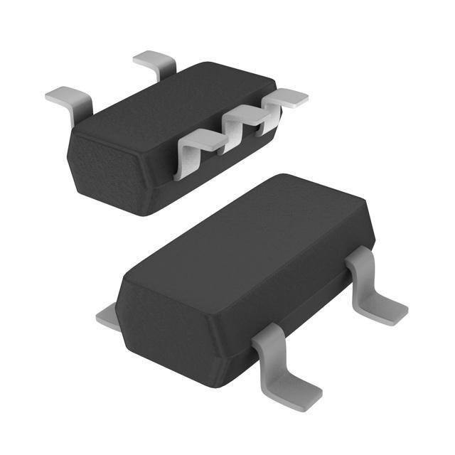
| 描述 | IC SWITCH SPST 5TSOP模拟开关 IC 3.3V SINGLE ANALOG |
| 产品分类 | |
| 品牌 | NXP Semiconductors |
| 产品手册 | |
| 产品图片 |
|
| rohs | 符合RoHS无铅 / 符合限制有害物质指令(RoHS)规范要求 |
| 产品系列 | 开关 IC,模拟开关 IC,NXP Semiconductors 74AHCT1G66GV,12574AHCT |
| 数据手册 | |
| 产品型号 | 74AHCT1G66GV,125 |
| 产品种类 | 模拟开关 IC |
| 供应商器件封装 | 5-TSOP |
| 其它名称 | 568-9106-1 |
| 功能 | |
| 包装 | 剪切带 (CT) |
| 商标 | NXP Semiconductors |
| 安装类型 | 表面贴装 |
| 安装风格 | SMD/SMT |
| 导通电阻 | 22 欧姆 |
| 导通电阻—最大值 | 148 Ohms |
| 封装 | Reel |
| 封装/外壳 | SC-74A,SOT-753 |
| 封装/箱体 | SOT-753 |
| 工作温度 | -40°C ~ 125°C |
| 工作电源电压 | 5 V |
| 工厂包装数量 | 3000 |
| 开关配置 | SPST |
| 最大功率耗散 | 250 mW |
| 最大工作温度 | + 125 C |
| 最小工作温度 | - 40 C |
| 标准包装 | 1 |
| 电压-电源,单/双 (±) | 4.5 V ~ 5.5 V |
| 电压源 | 单电源 |
| 电流-电源 | 1µA |
| 电源电压-最大 | 5.5 V |
| 电源电压-最小 | 4.5 V |
| 电源电流—最大值 | 75 mA |
| 电路 | 1 x SPST - NO |
| 空闲时间—最大值 | 11 ns |
| 运行时间—最大值 | 10 ns |
| 零件号别名 | 74AHCT1G66GV |


PDF Datasheet 数据手册内容提取
74AHC1G66; 74AHCT1G66 Single-pole single-throw analog switch Rev. 04 — 18 December 2008 Product data sheet 1. General description 74AHC1G66 and 74AHCT1G66 are high-speed Si-gate CMOS devices. They are single-pole single-throw analog switches. The switch has two input/output pins (YandZ) and an active HIGH enable input pin (E). When pinE is LOW, the analog switch is turned off. 2. Features n Very low ON resistance: u 26W (typ.)atV =3.0V CC u 16W (typ.)atV =4.5V CC u 14W (typ.)atV =5.5V CC n High noise immunity n Low power dissipation n Balanced propagation delays n Multiple package options n ESD protection: u HMB JESD22-A114E exceeds 2000 V u MM JESD22-A115-A exceeds 200 V u CDM JESD22-C101C exceeds 1000 V n Specified from-40 (cid:176)Cto+85(cid:176)C and -40 (cid:176)Cto+125 (cid:176)C 3. Ordering information Table 1. Ordering information Type number Package Temperature range Name Description Version 74AHC1G66GW -40 (cid:176)C to +125 (cid:176)C TSSOP5 plastic thin shrink small outline package; SOT353-1 5leads; body width1.25mm 74AHCT1G66GW 74AHC1G66GV -40 (cid:176)C to +125 (cid:176)C SC-74A plastic surface-mounted package; 5 leads SOT753 74AHCT1G66GV
74AHC1G66; 74AHCT1G66 Nexperia Single-pole single-throw analog switch 4. Marking Table 2. Marking codes Type number Marking 74AHC1G66GW AL 74AHCT1G66GW CL 74AHC1G66GV A66 74AHCT1G66GV C66 5. Functional diagram Z E E Y Z Y 001aag487 VCC mna628 Fig 1. Logic symbol Fig 2. Logic diagram 6. Pinning information 6.1 Pinning 74AHC1G66 74AHCT1G66 Y 1 5 VCC Z 2 GND 3 4 E 001aai834 Fig 3. Pin configuration SOT353-1 and SOT753 74AHC_AHCT1G66_4 © Nexperia B.V. 2017. All rights reserved Product data sheet Rev. 04 — 18 December 2008 2 of 17
74AHC1G66; 74AHCT1G66 Nexperia Single-pole single-throw analog switch 6.2 Pin description Table 3. Pin description Symbol Pin Description Y 1 independent input or output Z 2 independent input or output GND 3 ground (0 V) E 4 enable input(active HIGH) V 5 supply voltage CC 7. Functional description Table 4. Function table[1] InputE Switch L OFF H ON [1] H=HIGH voltage level; L=LOWvoltage level. 8. Limiting values Table 5. Limiting values In accordance with the Absolute Maximum Rating System (IEC 60134). Voltages are referenced to GND (ground = 0 V). Symbol Parameter Conditions Min Max Unit V supply voltage - 0.5 +7.0 V CC I input clamping current V <-0.5V [1] - 20 - mA IK I I switch clamping current V <-0.5 V or V >V + 0.5 V [1] - –20 mA SK I I CC I switch current -0.5 V < V < V +0.5 V - –25 mA SW O CC I supply current - 75 mA CC I ground current - 75 - mA GND T storage temperature - 65 +150 (cid:176)C stg P total power dissipation T =-40 (cid:176)Cto+125 (cid:176)C [2] - 250 mW tot amb [1] The input and output voltage ratings may be exceeded if the input and output voltage ratings are observed. [2] For TSSOP5 and SC-74A packages: above 87.5(cid:176)C the value of P derates linearly with 4.0mW/K. tot 9. Recommended operating conditions Table 6. Recommended operating conditions Voltages are referenced to GND (ground = 0 V).[1] Symbol Parameter Conditions 74AHC1G66 74AHCT1G66 Unit Min Typ Max Min Typ Max V supply voltage 2.0 5.0 5.5 4.5 5.0 5.5 V CC V input voltage 0 - 5.5 0 - 5.5 V I V switch voltage 0 - V 0 - V V SW CC CC 74AHC_AHCT1G66_4 © Nexperia B.V. 2017. All rights reserved Product data sheet Rev. 04 — 18 December 2008 3 of 17
74AHC1G66; 74AHCT1G66 Nexperia Single-pole single-throw analog switch Table 6. Recommended operating conditions …continued Voltages are referenced to GND (ground = 0 V).[1] Symbol Parameter Conditions 74AHC1G66 74AHCT1G66 Unit Min Typ Max Min Typ Max T ambient temperature -40 +25 +125 -40 +25 +125 (cid:176)C amb Dt/DV inputtransitionriseand V = 3.3– 0.3V [2] - - 100 - - - ns/V CC fall rate V = 5.0– 0.5V [2] - - 20 - - 20 ns/V CC [1] To avoid drawing V current out of pinZ, when switch current flows in pinY, the voltage drop across the bidirectional switch must not CC exceed 0.4V. If the switch current flows into pinZ, no V current will flow out of terminalY. In this case there is no limit for the voltage CC drop across the switch, but the voltage at pinsYandZ may not exceed V or GND. CC [2] Applies to control signal levels. 10. Static characteristics Table 7. Static characteristics Voltages are referenced to GND (ground = 0 V). Symbol Parameter Conditions 25(cid:176)C -40 (cid:176)C to+85 (cid:176)C -40 (cid:176)C to+125 (cid:176)C Unit Min Typ Max Min Max Min Max 74AHC1G66 V HIGH-level V = 2.0 V 1.5 - - 1.5 - 1.5 - V IH CC input voltage V = 3.0 V 2.1 - - 2.1 - 2.1 - V CC V = 5.5 V 3.85 - - 3.85 - 3.85 - V CC V LOW-level V = 2.0 V - - 0.5 - 0.5 - 0.5 V IL CC input voltage V = 3.0 V - - 0.9 - 0.9 - 0.9 V CC V = 5.5 V - - 1.65 - 1.65 - 1.65 V CC I input leakage V =5.5VorGND; - - 0.1 - 1.0 - 2.0 m A I I current V =5.5V CC I OFF-state Y or Z; V =5.5V; - - 0.1 - 1.0 - 4.0 m A S(OFF) CC leakage seeFigure4 current I ON-state Y or Z; V = 5.5 V; - - 0.1 - 1.0 - 4.0 m A S(ON) CC leakage seeFigure5 current I supply current E, Y or Z =V orGND; - - 1.0 - 10 - 40 m A CC CC V =5.5 V CC C input E input - 2.0 10 - 10 - 10 pF I capacitance C ON-state Y or Z input or output - 4.0 10 - 10 - 10 pF S(ON) capacitance 74AHCT1G66 V HIGH-level V = 4.5 V to 5.5 V 2.0 - - 2.0 - 2.0 - V IH CC input voltage V LOW-level V = 4.5 V to 5.5 V - - 0.8 - 0.8 - 0.8 V IL CC input voltage I input leakage V =5.5VorGND; - - 0.1 - 1.0 - 2.0 m A I I current V =5.5V CC 74AHC_AHCT1G66_4 © Nexperia B.V. 2017. All rights reserved Product data sheet Rev. 04 — 18 December 2008 4 of 17
74AHC1G66; 74AHCT1G66 Nexperia Single-pole single-throw analog switch Table 7. Static characteristics …continued Voltages are referenced to GND (ground = 0 V). Symbol Parameter Conditions 25(cid:176)C -40 (cid:176)C to+85 (cid:176)C -40 (cid:176)C to+125 (cid:176)C Unit Min Typ Max Min Max Min Max I OFF-state Y or Z; V =5.5V; - - 0.1 - 1.0 - 4.0 m A S(OFF) CC leakage seeFigure4 current I ON-state Y or Z; V = 5.5 V; - - 0.1 - 1.0 - 4.0 m A S(ON) CC leakage seeFigure5 current I supply current E, Y or Z =V orGND; - - 1.0 - 10 - 40 m A CC CC V =5.5 V CC DI additional per input pin; V =3.4V; - - 1.35 - 1.5 - 1.5 mA CC I supply current otherinputs at V orGND; CC I =0 A; V = 5.5 V O CC C input E input - 2.0 10 - 10 - 10 pF I capacitance C ON-state Y or Z input or output - 4.0 10 - 10 - 10 pF S(ON) capacitance 10.1 Test circuits VCC VCC E E VIL VIH Y Z Y Z IS IS IS VI GND VO VI GND VO 001aai835 001aai836 V = V or GND and V = GND or V . V = V or GND and V = open circuit. I CC O CC I CC O Fig 4. Test circuit for measuring OFF-state Fig 5. Test circuit for measuring ON-state leakagecurrent leakagecurrent 74AHC_AHCT1G66_4 © Nexperia B.V. 2017. All rights reserved Product data sheet Rev. 04 — 18 December 2008 5 of 17
74AHC1G66; 74AHCT1G66 Nexperia Single-pole single-throw analog switch 10.2 ON resistance Table 8. ON resistance At recommended operating conditions; voltages are referenced to GND (ground0V); for graph seeFigure7[1]. Symbol Parameter Conditions 25(cid:176)C -40 (cid:176)C to+85 (cid:176)C -40 (cid:176)C to+125 (cid:176) C Unit Typ max Max Max 74AHC1G66 and 74AHCT1G66 R ON resistance V =V to GND; seeFigure6 ON(peak) I CC (peak) I =1.0mA; V =2.0V 148[1] - - - W SW CC I =10mA;V =3.0Vto3.6V 28 50 70 110 W SW CC I =10mA;V =4.5Vto5.5V 15 30 40 60 W SW CC R ON resistance V =GND; seeFigure6 ON(rail) I (rail) I =1.0mA; V =2.0V 30 - - - W SW CC I =10mA;V =3.0Vto3.6V 20 50 65 90 W SW CC I =10mA;V =4.5Vto5.5V 15 22 26 40 W SW CC V =V ; seeFigure6 I CC I =1.0mA; V =2.0V 28 - - - W SW CC I =10mA;V =3.0Vto3.6V 18 50 65 90 W SW CC I =10mA;V =4.5Vto5.5V 13 22 26 40 W SW CC [1] At supply voltages approaching 2V, the analog switch ON resistance becomes extremely non-linear. Therefore it is recommended that these devices be used to transmit digital signals only, when using this supply voltage. 10.3 ON resistance test circuit and graphs mna630 40 RON (W ) 30 VSW VCC = 3.0 V VCC 20 4.5 V VIH E 5.5 V Y Z 10 VI GND ISW 0 0 2 4 6 001aag490 VI (V) R =V / I . T =25(cid:176)C. ON SW SW amb Fig 6. Test circuit for measuring ON resistance Fig 7. Typical ON resistance as a function of inputvoltage 74AHC_AHCT1G66_4 © Nexperia B.V. 2017. All rights reserved Product data sheet Rev. 04 — 18 December 2008 6 of 17
74AHC1G66; 74AHCT1G66 Nexperia Single-pole single-throw analog switch 11. Dynamic characteristics Table 9. Dynamic characteristics Voltages are referenced to GND (ground = 0 V);C =50pF; unless otherwise specified;Fortestcircuit seeFigure10. L Symbol Parameter Conditions 25(cid:176)C -40 (cid:176)C to +85 (cid:176)C -40 (cid:176)C to+125 (cid:176)C Unit Typ[1] max Max Max 74AHC1G66 t propagation YtoZ or ZtoY; seeFigure8 [2] pd delay V = 2.0 V 2.2 5.0 6.0 7.0 ns CC V = 3.0 V to 3.6V 1.0 2.0 3.0 4.0 ns CC V = 4.5V to 5.5V 0.6 1.0 2.0 3.0 ns CC t enable time EtoY or Z; seeFigure9 [2] en V = 2.0 V; C =15pF 7.0 25.0 33.0 40.0 ns CC L V = 2.0 V 11.0 35.0 46.0 57.0 ns CC V = 3.0 V to 3.6V; 4.0 11.0 14.0 18.0 ns CC C =15pF L V = 3.0 V to 3.6V 5.8 15.0 20.0 25.0 ns CC V = 4.5V to 5.5V; 3.0 8.0 10.0 13.0 ns CC C =15pF L V = 4.5V to 5.5V 4.0 11.0 13.0 17.0 ns CC t disable time EtoY or Z; seeFigure9 [2] dis V = 2.0 V; C =15pF 9.0 25.0 33.0 40.0 ns CC L V = 2.0 V 13.0 35.0 46.0 57.0 ns CC V = 3.0 V to 3.6V; 6.0 11.0 14.0 18.0 ns CC C =15pF L V = 3.0 V to 3.6V 8.4 15.0 20.0 25.0 ns CC V = 4.5V to 5.5V; 5.0 8.0 10.0 13.0 ns CC C =15pF L V = 4.5V to 5.5V 6.1 11.0 13.0 17.0 ns CC C power V =GNDtoV [3] 13 - - - pF PD I CC dissipation capacitance 74AHCT1G66 t propagation YtoZ or ZtoY; seeFigure8 [2] pd delay V = 4.5 V to 5.5 V 0.7 1.0 2.0 3.0 ns CC t enable time EtoY or Z; seeFigure9 [2] en V = 4.5 V to 5.5 V; 3.0 7.0 10.0 13.0 ns CC C =15pF L V = 4.5 V to 5.5 V 4.7 10.0 13.0 17.0 ns CC t disable time EtoY or Z; seeFigure9 [2] dis V =4.5V to 5.5 V; 5.0 8.0 10.0 13.0 ns CC C =15pF L V =4.5V to 5.5 V 6.5 11.0 13.0 17.0 ns CC 74AHC_AHCT1G66_4 © Nexperia B.V. 2017. All rights reserved Product data sheet Rev. 04 — 18 December 2008 7 of 17
74AHC1G66; 74AHCT1G66 Nexperia Single-pole single-throw analog switch Table 9. Dynamic characteristics …continued Voltages are referenced to GND (ground = 0 V);C =50pF; unless otherwise specified;Fortestcircuit seeFigure10. L Symbol Parameter Conditions 25(cid:176)C -40 (cid:176)C to +85 (cid:176)C -40 (cid:176)C to+125 (cid:176)C Unit Typ[1] max Max Max C power V =GNDtoV [3] 15 - - - pF PD I CC dissipation capacitance [1] All typical values are measured at V = 2.0 V, V = 3.3 V, V = 5.0 V and T =25(cid:176)C. CC CC CC amb [2] t is the same as t and t . pd PLH PHL t is the same as t and t . en PZL PZH t is the same as t and t . dis PLZ PHZ [3] C is used to determine the dynamic power dissipation P (mW). PD D P =C · V 2· f +S ((C · C )· V 2· f )where: D PD CC i L SW CC o f =input frequency in MHz; i f =output frequency in MHz; o C =output load capacitance in pF; L C =maximum switch capacitance in pF (seeTable7); SW V =supply voltage in Volt; CC S ((C · C )· V 2· f ) = sum of outputs. L SW CC o 11.1 Waveforms and test circuit VI Y or Z input VM GND tPLH tPHL VOH Z or Y output VM VOL mna667 Measurement points are given inTable10. Logic levels: V and V are typical output voltage levels that occur with the output load. OL OH Fig 8. Input (Y or Z) to output (Z or Y) propagation delays 74AHC_AHCT1G66_4 © Nexperia B.V. 2017. All rights reserved Product data sheet Rev. 04 — 18 December 2008 8 of 17
74AHC1G66; 74AHCT1G66 Nexperia Single-pole single-throw analog switch VI E VM GND tPLZ tPZL VCC output Y or Z LOW-to-OFF VM OFF-to-LOW VOL VX tPHZ tPZH VOH output VY Y or Z HIGH-to-OFF VM OFF-to-HIGH GND switch switch switch enabled disabled enabled mna668 Measurement points are given inTable10. Logic levels: V and V are typical output voltage levels that occur with the output load. OL OH Fig 9. Enable and disable times Table 10. Measurement points Type Input Output V V V V M M X Y 74AHC1G66 0.5V 0.5V V + 0.3V V - 0.3V CC CC OL OH 74AHCT1G66 1.5V 1.5V V + 0.3V V - 0.3V OL OH 74AHC_AHCT1G66_4 © Nexperia B.V. 2017. All rights reserved Product data sheet Rev. 04 — 18 December 2008 9 of 17
74AHC1G66; 74AHCT1G66 Nexperia Single-pole single-throw analog switch tW VI 90 % negative pulse VM VM 10 % 0 V tf tr tr tf VI 90 % positive pulse VM VM 10 % 0 V tW VCC VCC VI VO RL S1 G DUT open RT CL 001aad983 Test data is given inTable11. Definitions for test circuit: R = Termination resistance should be equal to output impedance Z of the pulse generator. T o C = Load capacitance including jig and probe capacitance. L R = Load resistance. L S1 = Test selection switch. Fig 10. Test circuit for measuring switching times Table 11. Test data Type Input Load S1 position V t, t C R t , t t , t t , t I r f L L PHL PLH PZH PHZ PZL PLZ 74AHC1G66 GND to V 3ns 15 pF, 50 pF 1 kW open GND V CC CC 74AHCT1G66 GND to 3V 3ns 15 pF, 50 pF 1 kW open GND V CC 11.2 Additional dynamic characteristics Table 12. Additional dynamic characteristics for 74AHC1G66 and 74AHCT1G66 GND = 0 V; t = t = 3.0 ns; C =50pF; unless otherwise specified. All typical values are measured at T =25(cid:176) C. r f L amb Symbol Parameter Conditions Min Typ Max Unit THD total harmonic f =1kHz; R = 10 kW; see Figure11 i L distortion V = 3.0 V to 3.6 V - 0.025 - % CC V = 4.5 V to 5.5 V - 0.015 - % CC f =10kHz; R = 10 kW; see Figure11 i L V = 3.0 V to 3.6 V; V = 2.5 V - 0.025 - % CC I V = 4.5 V to 5.5 V; V = 4.0 V - 0.015 - % CC I 74AHC_AHCT1G66_4 © Nexperia B.V. 2017. All rights reserved Product data sheet Rev. 04 — 18 December 2008 10 of 17
74AHC1G66; 74AHCT1G66 Nexperia Single-pole single-throw analog switch Table 12. Additional dynamic characteristics for 74AHC1G66 and 74AHCT1G66 …continued GND = 0 V; t = t = 3.0 ns; C =50pF; unless otherwise specified. All typical values are measured at T =25(cid:176) C. r f L amb Symbol Parameter Conditions Min Typ Max Unit f(- 3dB) -3dB frequency RL= 50W; C L=10pF; response seeFigure12and13 V = 3.0 V to 3.6 V - 230 - MHz CC V = 4.5 V to 5.5 V - 280 - MHz CC a isolation (OFF-state) R = 600W ; f =1MHz; seeFigure14 [1] iso L i V = 3.0 V to 3.6 V; V = 2.5 V - -50 - dB CC I V = 4.5 V to 5.5 V; V = 4.0 V - -50 - dB CC I [1] Adjust input voltage V to 0dBm level (0 dBm =1 mW into 50W ). I 11.3 Test circuits and graphs VCC VCC E VIH 2RL 10 m F Y/Z Z/Y VO fi 2RL CL D 001aai678 Test conditions: V = 3.0 V to 3.6 V; V = 2.5 V (p-p). CC I V = 4.5 V to 5.5 V; V = 4.0 V (p-p). CC I Fig 11. Test circuit for measuring total harmonic distortion VCC VCC E VIH 2RL 0.1 m F Y/Z Z/Y VO fi 2RL CL dB 001aai680 With f =1MHzadjusttheswitchinputvoltagefora0dBmlevelattheswitchoutput,(0dBm=1mWinto50W ).Thenincrease i the input f frequency until the dB meter reads- 3dB. i Fig 12. Test circuit for measuring the-3 dB frequency response 74AHC_AHCT1G66_4 © Nexperia B.V. 2017. All rights reserved Product data sheet Rev. 04 — 18 December 2008 11 of 17
74AHC1G66; 74AHCT1G66 Nexperia Single-pole single-throw analog switch 001aai837 4 (dB) 2 0 - 2 - 4 104 105 106 107 108 109 fi (Hz) Test conditions: V =4.5V; GND=0V; R =50W;R =1kW . CC L SOURCE Fig 13. Typical-3 dB frequency response VCC VCC E VIL 2RL 0.1 m F Y/Z Z/Y VO fi CL 2RL dB 001aai679 Adjust the switch input voltage for a 0 dBm level (0dBm = 1 mW into 600W ). Fig 14. Test circuit for measuring isolation (OFF-state) 74AHC_AHCT1G66_4 © Nexperia B.V. 2017. All rights reserved Product data sheet Rev. 04 — 18 December 2008 12 of 17
74AHC1G66; 74AHCT1G66 Nexperia Single-pole single-throw analog switch 12. Package outline TSSOP5: plastic thin shrink small outline package; 5 leads; body width 1.25 mm SOT353-1 D E A X c y HE v M A Z 5 4 A2 A A1 (A3) q 1 3 Lp L e w M bp e1 detail X 0 1.5 3 mm scale DIMENSIONS (mm are the original dimensions) UNIT mAax. A1 A2 A3 bp c D(1) E(1) e e1 HE L Lp v w y Z(1) q mm 1.1 0.1 1.0 0.15 0.30 0.25 2.25 1.35 0.65 1.3 2.25 0.425 0.46 0.3 0.1 0.1 0.60 7(cid:176) 0 0.8 0.15 0.08 1.85 1.15 2.0 0.21 0.15 0(cid:176) Note 1. Plastic or metal protrusions of 0.15 mm maximum per side are not included. OUTLINE REFERENCES EUROPEAN ISSUE DATE VERSION IEC JEDEC JEITA PROJECTION 00-09-01 SOT353-1 MO-203 SC-88A 03-02-19 Fig 15. Package outline SOT353-1 (TSSOP5) 74AHC_AHCT1G66_4 © Nexperia B.V. 2017. All rights reserved Product data sheet Rev. 04 — 18 December 2008 13 of 17
74AHC1G66; 74AHCT1G66 Nexperia Single-pole single-throw analog switch Plastic surface-mounted package; 5 leads SOT753 D B E A X y HE v M A 5 4 Q A A1 c 1 2 3 Lp detail X e bp w M B 0 1 2 mm scale DIMENSIONS (mm are the original dimensions) UNIT A A1 bp c D E e HE Lp Q v w y 1.1 0.100 0.40 0.26 3.1 1.7 3.0 0.6 0.33 mm 0.95 0.2 0.2 0.1 0.9 0.013 0.25 0.10 2.7 1.3 2.5 0.2 0.23 OUTLINE REFERENCES EUROPEAN ISSUE DATE VERSION IEC JEDEC JEITA PROJECTION 02-04-16 SOT753 SC-74A 06-03-16 Fig 16. Package outline SOT753 (SC-74A) 74AHC_AHCT1G66_4 © Nexperia B.V. 2017. All rights reserved Product data sheet Rev. 04 — 18 December 2008 14 of 17
74AHC1G66; 74AHCT1G66 Nexperia Single-pole single-throw analog switch 13. Abbreviations Table 13. Abbreviations Acronym Description CDM Charged Device Model CMOS Complementary Metal-Oxide Semiconductor DUT Device Under Test ESD ElectroStatic Discharge HBM Human Body Model MM Machine Model 14. Revision history Table 14. Revision history Document ID Release date Data sheet status Change notice Supersedes 74AHC_AHCT1G66_4 20081218 Product data sheet - 74AHC_AHCT1G66_3 Modifications: • The format of this data sheet has been redesigned to comply with the new identity guidelines of NXP Semiconductors. • Legal texts have been adapted to the new company name where appropriate. • Package SOT353 changed to SOT353-1 inTable1 andFigure15. • Quick Reference Data and Soldering sections removed. • Section 2 “Features” updated. 74AHC_AHCT1G66_3 20020606 Product specification - 74AHC_AHCT1G66_2 74AHC_AHCT1G66_2 20020215 Product specification - 74AHC_AHCT1G66_1 74AHC_AHCT1G66_1 20010129 Product specification - - 74AHC_AHCT1G66_4 © Nexperia B.V. 2017. All rights reserved Product data sheet Rev. 04 — 18 December 2008 15 of 17
74AHC1G66; 74AHCT1G66 Nexperia Single-pole single-throw analog switch 15. Legal information 15.1 Data sheet status Document status[1][2] Product status[3] Definition Objective [short] data sheet Development This document contains data from the objective specification for product development. Preliminary [short] data sheet Qualification This document contains data from the preliminary specification. Product [short] data sheet Production This document contains the product specification. [1] Please consult the most recently issued document before initiating or completing a design. [2] The term ‘short data sheet’ is explained in section “Definitions”. [3] Theproductstatusofdevice(s)describedinthisdocumentmayhavechangedsincethisdocumentwaspublishedandmaydifferincaseofmultipledevices.Thelatestproductstatus information is available on the Internet at URLhttp://www.nexperia.com. 15.2 Definitions malfunction of a Nexperia product can reasonably be expected to result in personal injury, death or severe property or environmental damage. Nexperia accepts no liability for inclusion and/or use of Draft —The document is a draft version only. The content is still under Nexperia products in such equipment or applications and internal review and subject to formal approval, which may result in therefore such inclusion and/or use is at the customer’s own risk. modifications or additions. Nexperia does not give any representations or warranties as to the accuracy or completeness of Applications —Applications that are described herein for any of these informationincludedhereinandshallhavenoliabilityfortheconsequencesof products are for illustrative purposes only. Nexperia makes no use of such information. representation or warranty that such applications will be suitable for the specified use without further testing or modification. Short data sheet —A short data sheet is an extract from a full data sheet withthesameproducttypenumber(s)andtitle.Ashortdatasheetisintended Limiting values —Stress above one or more limiting values (as defined in forquickreferenceonlyandshouldnotbereliedupontocontaindetailedand theAbsoluteMaximumRatingsSystemofIEC60134)maycausepermanent full information. For detailed and full information see the relevant full data damagetothedevice.Limitingvaluesarestressratingsonlyandoperationof sheet, which is available on request via the local Nexperia sales the device at these or any other conditions above those given in the office. In case of any inconsistency or conflict with the short data sheet, the Characteristics sections of this document is not implied. Exposure to limiting full data sheet shall prevail. values for extended periods may affect device reliability. Terms and conditions of sale —Nexperia products are sold 15.3 Disclaimers subjecttothegeneraltermsandconditionsofcommercialsale,aspublished athttp://www.nexperia.com/profile/terms, including those pertaining to warranty, intellectual property rights infringement and limitation of liability, unless General —Information in this document is believed to be accurate and explicitly otherwise agreed to in writing by Nexperia. In case of reliable.However,Nexperiadoesnotgiveanyrepresentationsor any inconsistency or conflict between information in this document and such warranties,expressedorimplied,astotheaccuracyorcompletenessofsuch terms and conditions, the latter will prevail. information and shall have no liability for the consequences of use of such No offer to sell or license —Nothing in this document may be interpreted information. or construed as an offer to sell products that is open for acceptance or the Right to make changes —Nexperiareservestherighttomake grant,conveyanceorimplicationofanylicenseunderanycopyrights,patents changes to information published in this document, including without or other industrial or intellectual property rights. limitation specifications and product descriptions, at any time and without notice.Thisdocumentsupersedesandreplacesallinformationsuppliedprior to the publication hereof. 15.4 Trademarks Suitability for use —Nexperia products are not designed, Notice:Allreferencedbrands,productnames,servicenamesandtrademarks authorized or warranted to be suitable for use in medical, military, aircraft, are the property of their respective owners. space or life support equipment, nor in applications where failure or 16. Contact information For more information, please visit:http://www.nexperia.com For sales office addresses, please send an email to:salesaddresses@nexperia.com 74AHC_AHCT1G66_4 © Nexperia B.V. 2017. All rights reserved Product data sheet Rev. 04 — 18 December 2008 16 of 17
74AHC1G66; 74AHCT1G66 Nexperia Single-pole single-throw analog switch 17. Contents 1 General description. . . . . . . . . . . . . . . . . . . . . . 1 2 Features . . . . . . . . . . . . . . . . . . . . . . . . . . . . . . . 1 3 Ordering information. . . . . . . . . . . . . . . . . . . . . 1 4 Marking. . . . . . . . . . . . . . . . . . . . . . . . . . . . . . . . 2 5 Functional diagram . . . . . . . . . . . . . . . . . . . . . . 2 6 Pinning information. . . . . . . . . . . . . . . . . . . . . . 2 6.1 Pinning . . . . . . . . . . . . . . . . . . . . . . . . . . . . . . . 2 6.2 Pin description . . . . . . . . . . . . . . . . . . . . . . . . . 3 7 Functional description . . . . . . . . . . . . . . . . . . . 3 8 Limiting values. . . . . . . . . . . . . . . . . . . . . . . . . . 3 9 Recommended operating conditions. . . . . . . . 3 10 Static characteristics. . . . . . . . . . . . . . . . . . . . . 4 10.1 Test circuits. . . . . . . . . . . . . . . . . . . . . . . . . . . . 5 10.2 ON resistance. . . . . . . . . . . . . . . . . . . . . . . . . . 6 10.3 ON resistance test circuit and graphs. . . . . . . . 6 11 Dynamic characteristics . . . . . . . . . . . . . . . . . . 7 11.1 Waveforms and test circuit . . . . . . . . . . . . . . . . 8 11.2 Additional dynamic characteristics . . . . . . . . . 10 11.3 Test circuits and graphs . . . . . . . . . . . . . . . . . 11 12 Package outline . . . . . . . . . . . . . . . . . . . . . . . . 13 13 Abbreviations. . . . . . . . . . . . . . . . . . . . . . . . . . 15 14 Revision history. . . . . . . . . . . . . . . . . . . . . . . . 15 15 Legal information. . . . . . . . . . . . . . . . . . . . . . . 16 15.1 Data sheet status . . . . . . . . . . . . . . . . . . . . . . 16 15.2 Definitions. . . . . . . . . . . . . . . . . . . . . . . . . . . . 16 15.3 Disclaimers. . . . . . . . . . . . . . . . . . . . . . . . . . . 16 15.4 Trademarks. . . . . . . . . . . . . . . . . . . . . . . . . . . 16 16 Contact information. . . . . . . . . . . . . . . . . . . . . 16 17 Contents. . . . . . . . . . . . . . . . . . . . . . . . . . . . . . 17 © Nexperia B.V. 2017. All rights reserved For more information, please visit: http://www.nexperia.com For sales office addresses, please send an email to: salesaddresses@nexperia.com Date of release: 18 December 2008