ICGOO在线商城 > 集成电路(IC) > 逻辑 - FIFO 存储器 > 7206L15J
 Datasheet下载
- 型号: 7206L15J
- 制造商: Integrated Device Technology
- 库位|库存: xxxx|xxxx
- 要求:
| 数量阶梯 | 香港交货 | 国内含税 |
| +xxxx | $xxxx | ¥xxxx |
查看当月历史价格
查看今年历史价格
7206L15J产品简介:
ICGOO电子元器件商城为您提供7206L15J由Integrated Device Technology设计生产,在icgoo商城现货销售,并且可以通过原厂、代理商等渠道进行代购。 7206L15J价格参考。Integrated Device Technology7206L15J封装/规格:逻辑 - FIFO 存储器, 。您可以下载7206L15J参考资料、Datasheet数据手册功能说明书,资料中有7206L15J 详细功能的应用电路图电压和使用方法及教程。
IDT(Integrated Device Technology Inc.)的7206L15J是一款高速FIFO(First-In-First-Out)存储器,属于逻辑类集成电路中的先进先出存储器类别。该器件广泛应用于需要高速数据缓冲和传输的场景。

其主要应用场景包括:

1. 通信系统:如网络交换设备、路由器和基站模块中,用于缓存高速传输的数据流,确保数据顺序正确并减少延迟。

2. 图像处理设备:在视频采集与显示系统中,用于缓冲图像数据,保持数据流的同步与稳定。

3. 工业控制与自动化:用于PLC(可编程逻辑控制器)或数据采集系统中,实现多模块间的数据缓冲与速率匹配。

4. 测试与测量仪器:如示波器、逻辑分析仪等,用于暂存高速采集的数据,便于后续处理与分析。

5. 计算机外围设备:如高速打印机、扫描仪等,用于协调主控单元与外设之间的数据传输速度差异。

7206L15J具有高速访问时间、低功耗和工业级工作温度范围,适合在高性能和可靠性要求较高的系统中使用。
| 参数 | 数值 |
| 品牌 | IDT |
| 产品目录 | 半导体 |
| 描述 | 先进先出 16K X 9 CMOS PARALLEL FIF |
| 产品分类 | 集成电路 - IC |
| 产品手册 | http://www.idt.com/document/dst/7203-7208-datasheet |
| 产品图片 |
|
| rohs | 否 |
| 产品系列 | 内存,先进先出,IDT 7206L15J |
| 产品型号 | 7206L15J |
| 产品种类 | 先进先出 |
| 商标 | IDT |
| 存储容量 | 144 kb |
| 安装风格 | SMD/SMT |
| 定时类型 | Asynchronous |
| 封装 | Tube |
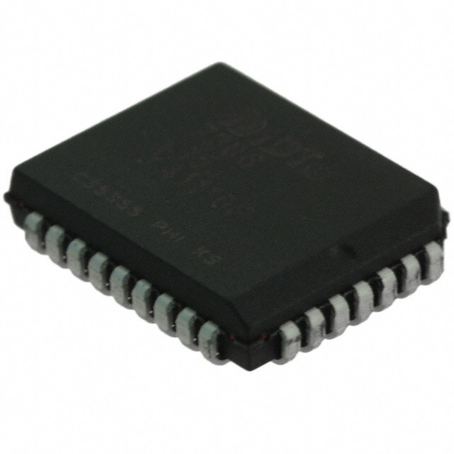
| 封装/箱体 | PLCC-32 |
| 工厂包装数量 | 32 |
| 总线定向 | Unidirectional |
| 数据总线宽度 | 9 bit |
| 最大工作温度 | + 70 C |
| 最大工作电流 | 120 mA |
| 最大时钟频率 | 40 MHz |
| 最小工作温度 | 0 C |
| 电源电压-最大 | 5.5 V |
| 电源电压-最小 | 4.5 V |
| 电路数量 | 2 |
| 系列 | 7206 |
| 组织 | 16 k x 9 |
| 访问时间 | 15 ns |
| 零件号别名 | 7206 IDT7206L15J |


- 商务部:美国ITC正式对集成电路等产品启动337调查
- 曝三星4nm工艺存在良率问题 高通将骁龙8 Gen1或转产台积电
- 太阳诱电将投资9.5亿元在常州建新厂生产MLCC 预计2023年完工
- 英特尔发布欧洲新工厂建设计划 深化IDM 2.0 战略
- 台积电先进制程称霸业界 有大客户加持明年业绩稳了
- 达到5530亿美元!SIA预计今年全球半导体销售额将创下新高
- 英特尔拟将自动驾驶子公司Mobileye上市 估值或超500亿美元
- 三星加码芯片和SET,合并消费电子和移动部门,撤换高东真等 CEO
- 三星电子宣布重大人事变动 还合并消费电子和移动部门
- 海关总署:前11个月进口集成电路产品价值2.52万亿元 增长14.8%


PDF Datasheet 数据手册内容提取
IDT7203 CMOS ASYNCHRONOUS FIFO IDT7204 2,048 x 9, 4,096 x 9 IDT7205 8,192 x 9, 16,384 x 9 IDT7206 32,768 x 9 and 65,536 x 9 IDT7207 IDT7208 LEAD FINISH (SnPb) ARE IN EOL PROCESS - LAST TIME BUY EXPIRES JUNE 15, 2018 FEATURES: • Industrial temperature range (–40°C to +85°C) is available (plastic packages only) ••••• First-In/First-Out Dual-Port memory ••••• 2,048 x 9 organization (IDT7203) ••••• Green parts available, see ordering information ••••• 4,096 x 9 organization (IDT7204) ••••• 8,192 x 9 organization (IDT7205) DESCRIPTION: ••••• 16,384 x 9 organization (IDT7206) The IDT7203/7204/7205/7206/7207/7208 are dual-port memory buffers ••••• 32,768 x 9 organization (IDT7207) with internal pointers that load and empty data on a first-in/first-out basis. The ••••• 65,636 x 9 organization (IDT7208) device uses Full and Empty flags to prevent data overflow and underflow and ••••• High-speed: 12ns access time expansion logic to allow for unlimited expansion capability in both word size and ••••• Low power consumption depth. — Active: 660mW (max.) Data is toggled in and out of the device through the use of the Write (W) and — Power-down: 44mW (max.) Read (R) pins. ••••• Asynchronous and simultaneous read and write The device's 9-bit width provides a bit for a control or parity at the user’s ••••• Fully expandable in both word depth and width option. It also features a Retransmit (RT) capability that allows the read pointer ••••• 720x family is pin and functionally compatible from 256 x 9 to 64k x 9 to be reset to its initial position when RT is pulsed LOW. A Half-Full Flag is ••••• Status Flags: Empty, Half-Full, Full available in the single device and width expansion modes. ••••• Retransmit capability These FIFOs are fabricated using high-speed CMOS technology. They ••••• High-performance CMOS technology are designed for applications requiring asynchronous and simultaneous read/ ••••• Military product compliant to MIL-STD-883, Class B writes in multiprocessing, rate buffering and other applications. ••••• Standard Military Drawing for #5962-88669 (IDT7203), 5962-89567 Military grade product is manufactured in compliance with MIL-STD-883, (IDT7203), and 5962-89568 (IDT7204) are listed on this function Class B. FUNCTIONAL BLOCK DIAGRAM DATA INPUTS (D0 -D8) WRITE W CONTROL RAM ARRAY WRITE 2,048 x 9 READ POINTER 4,096 x 9 POINTER 8,192 x 9 16,384 x 9 32,768 x 9 65,536 x 9 THREE- STATE BUFFERS RS DATA OUTPUTS R CORNETARDOL (Q 0 - Q8 ) RESET LOGIC FLAG LOGIC EF FL/RT FF EXPANSION XI LOGIC XO/HF 2661 drw01 IDT and the IDT logo are registered trademarks of Integrated Device Technology, Inc. COMMERCIAL, MILITARY AND INDUSTRIAL TEMPERATURE RANGES NOVEMBER 2017 1 © 2017 Integrated Device Technology, Inc. All rights reserved. Product subject to change without notice. DSC-2661/19
IDT7203/7204/7205/7206/7207/7208 CMOS ASYNCHRONOUS FIFO COMMERCIAL, INDUSTRIAL AND MILITARY 2,048 x 9, 4,096 x 9, 8,192 x 9, 16,384 x 9, 32,768 x 9 and 65,536 x 9 TEMPERATURE RANGES PIN CONFIGURATIONS W 1 28 Vcc INDEX D3D8WNCVccD4D5 D8 2 27 D4 4 3 2 2 10 D3 3 26 D5 D2 5 3 3329 D6 1 D2 4 25 D6 D1 6 28 D7 D1 5 24 D7 D0 7 27 NC D0 6 23 FL/RT XI 8 26 FL/RT XI RS FF 9 25 RS 7 22 FF 8 21 EF Q0 10 24 EF Q0 9 20 XO/HF Q1 11 23 XO/HF Q1 10 19 Q7 NQC2 1123 2221 QQ76 Q2 11 18 Q6 14 15 16 17 18 19 20 Q3 12 17 Q5 3 8DCR4 5 Q8 13 16 Q4 QQNN QQ GND 14 15 R G 2661 drw02b 2661 drw02a TOP VIEW TOP VIEW Reference Order Device Reference Order Device Package Type Identifier Code Availability Package Type Identifier Code Availability PLASTIC DIP P28-1 P All devices PLCC J32-1 J All devices PLASTIC THIN DIP P28-2 TP All except IDT7207/7208 LCC(1) L32-1 L All except IDT7208 CERDIP D28-1 D All except IDT7208 THIN CERDIP D28-3 TD Only for IDT7203/7204/7205 NOTE: SOIC SO28-3 SO Only for IDT7204 1. This package is only available in the military temperature range. RECOMMENDED DC OPERATING CONDITIONS Symbol Parameter Min. Typ. Max. Unit VCC Supply Voltage 4.5 5.0 5.5 V ABSOLUTE MAXIMUM RATINGS Commercial/Industrial/Military Symbol Rating Com'l & Ind'l Military Unit GND Supply Voltage 0 0 0 V VTERM Terminal –0.5 to +7.0 –0.5 to +7.0 V VIH(1) Input High Voltage 2.0 — — V Commercial/Industrial Voltage with Respect to GND VIH(1) Input High Voltage Military 2.2 — — V TSTG Storage –55 to + 125 –65 to +155 °C VIL(2) Input Low Voltage — — 0.8 V Temperature Commercial/Industrial/Military IOUT DC Output –50 to +50 –50 to +50 mA TA Operating Temperature Commercial 0 — 70 °C +Current TA Operating Temperature Industrial –40 — 85 °C NOTE: TA Operating Temperature Military –55 — 125 °C 1. Stresses greater than those listed under ABSOLUTE MAXIMUM RATINGS may cause permanent damage to the device. This is a stress rating only and functional operation NOTES: of the device at these or any other conditions above those indicated in the operational 1.For RT/RS/XI input, VIH = 2.6V (commercial). sections of this specification is not implied. Exposure to absolute maximum rating For RT/RS/XI input, VIH = 2.6V (military). conditions for extended periods may affect reliability. 2.1.5V undershoots are allowed for 10ns once per cycle. 2
IDT7203/7204/7205/7206/7207/7208 CMOS ASYNCHRONOUS FIFO COMMERCIAL, INDUSTRIAL AND MILITARY 2,048 x 9, 4,096 x 9, 8,192 x 9, 16,384 x 9, 32,768 x 9 and 65,536 x 9 TEMPERATURE RANGES DC ELECTRICAL CHARACTERISTICS (Commercial: VCC = 5V ± 10%, TA = 0°C to +70°C; Industrial: VCC = 5V ± 10%, TA = –40°C to +85°C; Military: VCC = 5V ± 10%, TA = –55°C to +125°C) IDT7203(1) IDT7203 IDT7204(1) IDT7204 Commercial and Industrial Military(3) tA = 12, 15, 20, 25, 35, 50 ns tA = 20, 30, 40 ns Symbol Parameter Min. Typ. Max. Min. Typ. Max. Unit ILI(6) Input Leakage Current (Any Input) –1 — 1 –1 — 1 μA ILO(7) Output Leakage Current –10 — 10 –10 — 10 μA VOH Output Logic “1” Voltage IOH = –2mA 2.4 — — 2.4 — — V VOL Output Logic “0” Voltage IOL = 8mA — — 0.4 — — 0.4 V ICC1(8,9,10) Active Power Supply Current — — 120 — — 150 mA ICC2(8,10,11) Standby Current (R=W=RS=FL/RT=VIH) — — 12 — — 25 mA ICC3(8,10,12) Power Down Current — — 2 — — 4 mA IDT7205(1) IDT7205 IDT7206(2,4) IDT7206 IDT7207(2,4) IDT7207 IDT7208(2,5) Commercial and Industrial Military tA = 12, 15, 20, 25, 35, 50 ns tA = 20, 30 ns Symbol Parameter Min. Typ. Max. Min. Typ. Max. Unit ILI(6) Input Leakage Current (Any Input) –1 — 1 –1 — 1 μA ILO(7) Output Leakage Current –10 — 10 –10 — 10 μA VOH Output Logic “1” Voltage IOH = –2mA 2.4 — — 2.4 — — V VOL Output Logic “0” Voltage IOL = 8mA — — 0.4 — — 0.4 V ICC1(8,9,10) Active Power Supply Current — — 120 — — 150 mA ICC2(8,10,11) Standby Current (RS=FL/RT=VIH) — — 12 — — 25 mA ICC3(8,10,12) Power Down Current — — 8 — — 12 mA NOTES: 1.Industrial temperature range product for 15ns and 25ns speed grades are available 6. Measurements with 0.4 ≤ VIN ≤ VCC. as a standard device. 7. R ≥ VIH, 0.4 ≤ VOUT ≤ VCC. 2.Industrial temperature range product for 25ns speed grade only is available as a standard 8. Tested with outputs open (IOUT = 0). device. All other speed grades are available by special order. 9. R and W toggle at 20 MHz and data inputs switch at 10 MHz. 3.Military temperature range product for the 40ns is only available for 7203. 10.ICC measurements are made with outputs open. 4.Commercial temperature range product for the 12ns not available. 11.All Inputs = VCC - 0.2V or GND + 0.2V, except R and W, which toggle at 20MHz. 5.Commercial temperature range product for the 12ns, 15ns and 50ns not available. 12.All Inputs = VCC - 0.2V or GND + 0.2V, except R and W = VCC -0.2V. 5V AC TEST CONDITIONS Input Pulse Levels GND to 3.0V 1.1KΩ Input Rise/Fall Times 5ns Input Timing Reference Levels 1.5V Output Reference Levels 1.5V D.U.T. Output Load See Figure 1 680Ω 30pF* CAPACITANCE(1) (TA = +25°C, f = 1.0 MHz) Symbol Parameter Condition Max. Unit 2661 drw03 CIN(1) Input Capacitance VIN = 0V 10 pF or equivalent circuit COUT(1,2) Output Capacitance VOUT = 0V 10 pF NOTES: 1. This parameter is sampled and not 100% tested. Figure 1. Output Load 2. With output deselected. *Includes jig and scope capacitances. 3
IDT7203/7204/7205/7206/7207/7208 CMOS ASYNCHRONOUS FIFO COMMERCIAL, INDUSTRIAL AND MILITARY 2,048 x 9, 4,096 x 9, 8,192 x 9, 16,384 x 9, 32,768 x 9 and 65,536 x 9 TEMPERATURE RANGES AC ELECTRICAL CHARACTERISTICS(1) (Commercial: VCC = 5V ± 10%, TA = 0°C to +70°C; Industrial: VCC = 5V ± 10%, TA = –40°C to +85°C; Military: VCC = 5V ± 10%, TA = –55°C to +125°C) Commercial Com'l & Ind'l Com'l & Military Commercial Com'l & Ind'l IDT7203L12 IDT7203L15(2) IDT7203L20 IDT7208L20 IDT7203L25(2) IDT7204L12 IDT7204L15(2) IDT7204L20 IDT7204L25(2) IDT7205L12 IDT7205L15(2) IDT7205L20 IDT7205L25(2) IDT7206L15 IDT7206L20 IDT7206L25(3) IDT7207L15 IDT7207L20 IDT7207L25(3) IDT7208L25(3) Symbol Parameters Min. Max. Min. Max. Min. Max. Min. Max. Min. Max. Unit fS Shift Frequency — 50 — 40 — 33.3 — 33.3 — 28.5 MHz tRC Read Cycle Time 20 — 25 — 30 — 30 — 35 — ns tA Access Time — 12 — 15 — 20 — 20 — 25 ns tRR Read Recovery Time 8 — 10 — 10 — 10 — 10 — ns tRPW Read Pulse Width(4) 12 — 15 — 20 — 20 — 25 — ns tRLZ Read LOW to Data Bus LOW(5) 3 — 5 — 5 — 5 — 5 — ns tWLZ Write HIGH to Data Bus Low-Z(5,6) 3 — 5 — 5 — 5 — 5 — ns tDV Data Valid from Read HIGH 5 — 5 — 5 — 5 — 5 — ns tRHZ Read HIGH to Data Bus High-Z(5) — 12 — 15 — 15 — 15 — 18 ns tWC Write Cycle Time 20 — 25 — 30 — 30 — 35 — ns tWPW Write Pulse Width(4) 12 — 15 — 20 — 20 — 25 — ns tWR Write Recovery Time 8 — 10 — 10 — 10 — 10 — ns tDS Data Set-up Time 9 — 11 — 12 — 12 — 15 — ns tDH Data Hold Time 0 — 0 — 0 — 0 — 0 — ns tRSC Reset Cycle Time 20 — 25 — 30 — 30 — 35 — ns tRS Reset Pulse Width(4) 12 — 15 — 20 — 20 — 25 — ns tRSS Reset Set-up Time(5) 12 — 15 — 20 — 20 — 25 — ns tRTR Reset Recovery Time 8 — 10 — 10 — 10 — 10 — ns tRTC Retransmit Cycle Time 20 — 25 — 30 — 30 — 35 — ns tRT Retransmit Pulse Width(4) 12 — 15 — 20 — 20 — 25 — ns tRTS Retransmit Set-up Time(5) 12 — 15 — 20 — 20 — 25 — ns tRTR Retransmit Recovery Time 8 — 10 — 10 — 10 — 10 — ns tEFL Reset to EF LOW — 12 — 25 — 30 — 30 — 35 ns tHFH, tFFH Reset to HF and FF HIGH — 17 — 25 — 30 — 30 — 35 ns tRTF Retransmit LOW to Flags Valid — 20 — 25 — 30 — 30 — 35 ns tREF Read LOW to EF LOW — 12 — 15 — 20 — 20 — 25 ns tRFF Read HIGH to FF HIGH — 14 — 15 — 20 — 20 — 25 ns tRPE Read Pulse Width after EF HIGH 12 — 15 — 20 — 20 — 25 — ns tWEF Write HIGH to EF HIGH — 12 — 15 — 20 — 20 — 25 ns tWFF Write LOW to FF LOW — 14 — 15 — 20 — 20 — 25 ns tWHF Write LOW to HF Flag LOW — 17 — 25 — 30 — 30 — 35 ns tRHF Read HIGH to HF Flag HIGH — 17 — 25 — 30 — 30 — 35 ns tWPF Write Pulse Width after FF HIGH 12 — 15 — 20 — 20 — 25 — ns tXOL Read/Write LOW to XO LOW — 12 — 15 — 20 — 20 — 25 ns tXOH Read/Write HIGH to XO HIGH — 12 — 15 — 20 — 20 — 25 ns tXI XI Pulse Width(4) 12 — 15 — 20 — 20 — 25 — ns tXIR XI Recovery Time 8 — 10 — 10 — 10 — 10 — ns tXIS XI Set-up Time 8 — 10 — 10 — 10 — 10 — ns NOTES: 1. Timings referenced as in AC Test Conditions. 2. Industrial temperature range product for 15ns and 25ns speed grades are available as a standard device. 3. Industrial temperature range product for 25ns speed grade only is available as a standard device. All other speed grades are available by special order. 4. Pulse widths less than minimum are not allowed. 5. Values guaranteed by design, not currently tested. 6. Only applies to read data flow-through mode. 4
IDT7203/7204/7205/7206/7207/7208 CMOS ASYNCHRONOUS FIFO COMMERCIAL, INDUSTRIAL AND MILITARY 2,048 x 9, 4,096 x 9, 8,192 x 9, 16,384 x 9, 32,768 x 9 and 65,536 x 9 TEMPERATURE RANGES AC ELECTRICAL CHARACTERISTICS(1) (CONTINUED) (Commercial: VCC = 5V ± 10%, TA = 0°C to +70°C; Industrial: VCC = 5V ± 10%, TA = –40°C to +85°C; Military: VCC = 5V ± 10%, TA = –55°C to +125°C) Military Commercial Military Commercial IDT7203L30 IDT7203L35 IDT7203L40 IDT7203L50 IDT7204L30 IDT7204L35 IDT7204L50 IDT7205L30 IDT7205L35 IDT7205L50 IDT7206L30 IDT7206L35 IDT7206L50 IDT7207L30 IDT7207L35 IDT7207L50 IDT7208L35 Symbol Parameters Min. Max. Min. Max. Min. Max. Min. Max. Unit fS Shift Frequency — 25 — 22.22 — 20 — 15 MHz tRC Read Cycle Time 40 — 45 — 50 — 65 — ns tA Access Time — 30 — 35 — 40 — 50 ns tRR Read Recovery Time 10 — 10 — 10 — 15 — ns tRPW Read Pulse Width(2) 30 — 35 — 40 — 50 — ns tRLZ Read LOW to Data Bus LOW(3) 5 — 5 — 5 — 10 — ns tWLZ Write HIGH to Data Bus Low-Z(3,4) 5 — 10 — 10 — 15 — ns tDV Data Valid from Read HIGH 5 — 5 — 5 — 5 — ns tRHZ Read HIGH to Data Bus High-Z(3) — 20 — 20 — 25 — 30 ns tWC Write Cycle Time 40 — 45 — 50 — 65 — ns tWPW Write Pulse Width(2) 30 — 35 — 40 — 50 — ns tWR Write Recovery Time 10 — 10 — 10 — 15 — ns tDS Data Set-up Time 18 — 18 — 20 — 30 — ns tDH Data Hold Time 0 — 0 — 0 — 5 — ns tRSC Reset Cycle Time 40 — 45 — 50 — 65 — ns tRS Reset Pulse Width(2) 30 — 35 — 40 — 50 — ns tRSS Reset Set-up Time(3) 30 — 35 — 40 — 50 — ns tRTR Reset Recovery Time 10 — 10 — 10 — 15 — ns tRTC Retransmit Cycle Time 40 — 45 — 50 — 65 — ns tRT Retransmit Pulse Width(2) 30 — 35 — 40 — 50 — ns tRTS Retransmit Set-up Time(3) 30 — 35 — 40 — 50 — ns tRTR Retransmit Recovery Time 10 — 10 — 10 — 15 — ns tEFL Reset to EF LOW — 40 — 45 — 50 — 65 ns tHFH, tFFH Reset to HF and FF HIGH — 40 — 45 — 50 — 65 ns tRTF Retransmit LOW to Flags Valid — 40 — 45 — 50 — 65 ns tREF Read LOW to EF LOW — 30 — 30 — 35 — 45 ns tRFF Read HIGH to FF HIGH — 30 — 30 — 35 — 45 ns tRPE Read Pulse Width after EF HIGH 30 — 35 — 40 — 50 — ns tWEF Write HIGH to EF HIGH — 30 — 30 — 35 — 45 ns tWFF Write LOW to FF LOW — 30 — 30 — 35 — 45 ns tWHF Write LOW to HF Flag LOW — 40 — 45 — 50 — 65 ns tRHF Read HIGH to HF Flag HIGH — 40 — 45 — 50 — 65 ns tWPF Write Pulse Width after FF HIGH 30 — 35 — 40 — 50 — ns tXOL Read/Write LOW to XO LOW — 30 — 35 — 40 — 50 ns tXOH Read/Write HIGH to XO HIGH — 30 — 35 — 40 — 50 ns tXI XI Pulse Width(2) 30 — 35 — 40 — 50 — ns tXIR XI Recovery Time 10 — 10 — 10 — 10 — ns tXIS XI Set-up Time 10 — 15 — 15 — 15 — ns NOTES: 1. Timings referenced as in AC Test Conditions. 2. Pulse widths less than minimum are not allowed. 3. Values guaranteed by design, not currently tested. 4. Only applies to read data flow-through mode. 5
IDT7203/7204/7205/7206/7207/7208 CMOS ASYNCHRONOUS FIFO COMMERCIAL, INDUSTRIAL AND MILITARY 2,048 x 9, 4,096 x 9, 8,192 x 9, 16,384 x 9, 32,768 x 9 and 65,536 x 9 TEMPERATURE RANGES SIGNAL DESCRIPTIONS loaded (see Operating Modes). The Single Device Mode is initiated by grounding the Expansion In (XI). The IDT7203/7204/7205/7206/7207/7208 can be made to retransmit data INPUTS: when the Retransmit Enable Control (RT) input is pulsed LOW. A retransmit operation will set the internal read pointer to the first location and will not affect the DATA IN (D0–D8) — Data inputs for 9-bit wide data. write pointer. The status of the Flags will change depending on the relative locations of the read and write pointers. Read Enable (R) and Write Enable (W) must be CONTROLS: in the HIGH state during retransmit. This feature is useful when less than 2,048/ 4,096/8,192/16,384/32,768/65,536 writes are performed between resets. The RESET ( RS ) — Reset is accomplished whenever the Reset (RS) input is retransmit feature is not compatible with the Depth Expansion Mode. taken to a LOW state. During reset, both internal read and write pointers are set to the first location. A reset is required after power-up before a write operation can EXPANSION IN ( XI ) — This input is a dual-purpose pin. Expansion In (XI) take place. Both the Read Enable (R) and Write Enable (W) inputs must is grounded to indicate an operation in the single device mode. Expansion In (XI) be in the HIGH state during the window shown in Figure 2 (i.e. tRSS before is connected to Expansion Out (XO) of the previous device in the Depth Expansion the rising edge of RS) and should not change until tRSR after the rising or Daisy-Chain Mode. edge of RS. OUTPUTS: WRITE ENABLE ( W ) — A write cycle is initiated on the falling edge of this input if the Full Flag (FF) is not set. Data set-up and hold times must be adhered- FULL FLAG ( FF ) — The Full Flag (FF) will go LOW, inhibiting further write to, with respect to the rising edge of the Write Enable (W). Data is stored in the RAM operations, when the device is full. If the read pointer is not moved after Reset (RS), array sequentially and independently of any on-going read operation. the Full Flag (FF) will go LOW after 2,048/4,096/8,192/16,384/32,768/65,536 After half of the memory is filled, and at the falling edge of the next write operation, writes. the Half-Full Flag (HF) will be set to LOW, and will remain set until the difference between the write pointer and read pointer is less-than or equal to one-half of the EMPTY FLAG ( EF ) — The Empty Flag (EF) will go LOW, inhibiting further total memory of the device. The Half-Full Flag (HF) is then reset by the rising edge read operations, when the read pointer is equal to the write pointer, indicating that of the read operation. the device is empty. To prevent data overflow, the Full Flag (FF) will go LOW on the falling edge of the last write signal, which inhibits further write operations. Upon the completion EXPANSION OUT/HALF-FULL FLAG ( XO/HF ) — This is a dual-purpose of a valid read operation, the Full Flag (FF) will go HIGH after tRFF, allowing a output. In the single device mode, when Expansion In (XI) is grounded, this output new valid write to begin. When the FIFO is full, the internal write pointer is blocked acts as an indication of a half-full memory. from W, so external changes in W will not affect the FIFO when it is full. After half of the memory is filled, and at the falling edge of the next write operation, the Half-Full Flag (HF) will be set to LOW and will remain set until the difference READ ENABLE ( R ) — A read cycle is initiated on the falling edge of the Read between the write pointer and read pointer is less than or equal to one half of the Enable (R), provided the Empty Flag (EF) is not set. The data is accessed on total memory of the device. The Half-Full Flag (HF) is then reset by the rising edge a First-In/First-Out basis, independent of any ongoing write operations. After Read of the read operation. Enable (R) goes HIGH, the Data Outputs (Q0 through Q8) will return to a high- In the Depth Expansion Mode, Expansion In (XI) is connected to Expansion impedance condition until the next Read operation. When all the data has been Out (XO) of the previous device. This output acts as a signal to the next device read from the FIFO, the Empty Flag (EF) will go LOW, allowing the “final” read in the Daisy Chain by providing a pulse to the next device when the previous device cycle but inhibiting further read operations, with the data outputs remaining in a high- reaches the last location of memory. There will be an XO pulse when the Write impedance state. Once a valid write operation has been accomplished, the Empty pointer reaches the last location of memory, and an additional XO pulse when the Flag (EF) will go HIGH after tWEF and a valid Read can then begin. When the Read pointer reaches the last location of memory. FIFO is empty, the internal read pointer is blocked from R so external changes will not affect the FIFO when it is empty. DATA OUTPUTS (Q0-Q8) — Q0-Q8 are data outputs for 9-bit wide data. These outputs are in a high-impedance condition whenever Read (R) is in a HIGH FIRST LOAD/RETRANSMIT ( FL/RT ) — This is a dual-purpose input. In state. the Depth Expansion Mode, this pin is grounded to indicate that it is the first device 6
IDT7203/7204/7205/7206/7207/7208 CMOS ASYNCHRONOUS FIFO COMMERCIAL, INDUSTRIAL AND MILITARY 2,048 x 9, 4,096 x 9, 8,192 x 9, 16,384 x 9, 32,768 x 9 and 65,536 x 9 TEMPERATURE RANGES tRSC tRS RS tRSS tRSR W tRSS R tEFL EF tHFH, tFFH HF, FF 2661 drw04 NOTE: 1. W and R = VIH around the rising edge of RS. Figure 2. Reset tRC tRPW tA tRR tA R tRLZ tDV tRHZ Q0-Q8 DATAOUTVALID DATAOUTVALID tWC tWPW tWR W tDS tDH D0-D8 DATAINVALID DATAINVALID 2661 drw05 Figure 3. Asynchronous Write and Read Operation IGNORED LAST WRITE WRITE FIRST READ R W tRFF tWFF FF 2661 drw06 Figure 4. Full Flag Timing From Last Write to First Read 7
IDT7203/7204/7205/7206/7207/7208 CMOS ASYNCHRONOUS FIFO COMMERCIAL, INDUSTRIAL AND MILITARY 2,048 x 9, 4,096 x 9, 8,192 x 9, 16,384 x 9, 32,768 x 9 and 65,536 x 9 TEMPERATURE RANGES IGNORED LAST READ READ FIRST WRITE W R tREF tWEF EF tA DATA OUT VALID 2661 drw07 Figure 5. Empty Flag Timing From Last Read to First Write tRTC tRT RT tRTS tRTR W,R tRTF HF, EF, FF FLAG VALID 2661 drw08 NOTE: 1. EF, FF and HF may change status during Retransmit, but flags will be valid at tRTC. Figure 6. Retransmit W tWEF EF tRPE R 2661 drw09 Figure 7. Minimum Timing for an Empty Flag Coincident Read Pulse. R tRFF FF tWPF W 2661 drw10 Figure 8. Minimum Timing for a Full Flag Coincident Write Pulse. 8
IDT7203/7204/7205/7206/7207/7208 CMOS ASYNCHRONOUS FIFO COMMERCIAL, INDUSTRIAL AND MILITARY 2,048 x 9, 4,096 x 9, 8,192 x 9, 16,384 x 9, 32,768 x 9 and 65,536 x 9 TEMPERATURE RANGES W R tWHF tRHF HF HALF-FULL OR LESS MORE THAN HALF-FULL HALF-FULL OR LESS 2661 drw11 Figure 9. Half-Full Flag Timing WRITE TO W LAST PHYSICAL LOCATION READ FROM R LAST PHYSICAL LOCATION tXOL tXOH tXOL tXOH XO 2661 drw12 Figure 10. Expansion Out tXI tXIR XI tXIS WRITE TO W FIRST PHYSICAL LOCATION tXIS READ FROM R FIRST PHYSICAL LOCATION 2661 drw13 Figure 11. Expansion In OPERATING MODES: 7204/7205/7206/7207/7208s. These devices operate in the Depth Expansion Care must be taken to assure that the appropriate flag is monitored by mode when the following conditions are met: each system (i.e. FF is monitored on the device where W is used; EF is monitored 1. The first device must be designated by grounding the First Load (FL) control on the device where R is used). For additional information on the IDT7203/7204/ input. 7205/7206/7207, refer to Tech Note 8: Operating FIFOs on Full and Empty 2. All other devices must have FL in the HIGH state. Boundary Conditions and Tech Note 6: Designing with FIFOs. 3. The Expansion Out (XO) pin of each device must be tied to the Expansion Single Device Mode In (XI) pin of the next device. See Figure 14. A single IDT7203/7204/7205/7206/7207/7208 may be used when the 4. External logic is needed to generate a composite Full Flag (FF) and Empty application requirements are for 2,048/4,096/8,192/16,384/32,768/65,536 words Flag (EF). This requires the ORing of all EFs and ORing of all FFs (i.e. all or less. These FIFOs are in a Single Device Configuration when the Expansion must be set to generate the correct composite FF or EF). See Figure 14. In (XI) control input is grounded (see Figure 12). 5. The Retransmit (RT) function and Half-Full Flag (HF) are not available in Depth Expansion the Depth Expansion Mode. These FIFOs can easily be adapted to applications when the require- ments are for greater than 2,048/4,096/8,192/16,384/32,768/65,536 words. For additional information on the IDT7203/7204/7205/7206/7207, refer to Figure 14 demonstrates Depth Expansion using three IDT7203/7204/7205/ Tech Note 9: Cascading FIFOs or FIFO Modules. 7206/7207/7208s. Any depth can be attained by adding additional IDT7203/ 9
IDT7203/7204/7205/7206/7207/7208 CMOS ASYNCHRONOUS FIFO COMMERCIAL, INDUSTRIAL AND MILITARY 2,048 x 9, 4,096 x 9, 8,192 x 9, 16,384 x 9, 32,768 x 9 and 65,536 x 9 TEMPERATURE RANGES USAGE MODES: FIFO permits a reading of a single word after writing one word of data into an Width Expansion empty FIFO. The data is enabled on the bus in (tWEF + tA) ns after the rising edge of W, called the first write edge, and it remains on the bus until the R line Word width may be increased simply by connecting the corresponding input is raised from LOW-to-HIGH, after which the bus would go into a three-state control signals of multiple devices. Status flags (EF, FF and HF) can be detected from any one device. Figure 13 demonstrates an 18-bit word width by using mode after tRHZ ns. The EF line would have a pulse showing temporary deassertion and then would be asserted. two IDT7203/7204/7205/7206/7207/7208s. Any word width can be attained In the write flow-through mode (Figure 18), the FIFO permits the writing of by adding additional IDT7203/7204/7205/7206/7207/7208s (Figure 13). a single word of data immediately after reading one word of data from a full FIFO. The R line causes the FF to be deasserted but the W line being LOW causes Bidirectional Operation it to be asserted again in anticipation of a new data word. On the rising edge of Applications which require data buffering between two systems (each W, the new word is loaded in the FIFO. The W line must be toggled when FF system capable of Read and Write operations) can be achieved by pairing is not asserted to write new data in the FIFO and to increment the write pointer. IDT7203/7204/7205/7206/7207/7208s as shown in Figure 16. Both Depth Expansion and Width Expansion may be used in this mode. Compound Expansion The two expansion techniques described above can be applied together Data Flow-Through in a straightforward manner to achieve large FIFO arrays (see Figure 15). Two types of flow-through modes are permitted, a read flow-through and write flow-through mode. For the read flow-through mode (Figure 17), the (HALF-FULL FLAG) (HF) WRITE (W) IDT READ (R) 9 7203 9 DATA IN (D) 7204 DATA OUT (Q) 7205 FULL FLAG (FF) EMPTY FLAG (EF) 7206 RESET (RS) 7207 RETRANSMIT (RT) 7208 EXPANSION IN (XI) 2661 drw14 Figure 12. Block Diagram of 2,048 x 9, 4,096 x 9, 8,192 x 9, 16,384 x 9, 32,768 x 9, 65,536 x 9 FIFO Used in Single Device Mode HF HF 18 9 9 DATAIN (D) WRITE (W) IDT IDT READ (R) 7203 7203 7204 FULL FLAG (FF) 7204 7205 EMPTY FLAG (EF) 7205 7206 7206 RESET (RS) 7207 7207 7208 RETRANSMIT (RT) 7208 9 9 XI XI 18 DATA OUT (Q) NOTE: 2661 drw15 1. Flag detection is accomplished by monitoring the FF, EF and HF signals on either (any) device used in the width expansion configuration. Do not connect any output signals together. Figure 13. Block Diagram of 2,048 x 18, 4,096 x 18, 8,192 x 18, 16,384 x 18, 32,768 x 18, 65,536 x 18 FIFO Memory Used in Width Expansion Mode 10
IDT7203/7204/7205/7206/7207/7208 CMOS ASYNCHRONOUS FIFO COMMERCIAL, INDUSTRIAL AND MILITARY 2,048 x 9, 4,096 x 9, 8,192 x 9, 16,384 x 9, 32,768 x 9 and 65,536 x 9 TEMPERATURE RANGES TRUTH TABLES TABLE 1 – RESET AND RETRANSMIT SINGLE DEVICE CONFIGURATION/WIDTH EXPANSION MODE Inputs Internal Status Outputs Mode RS FL/RT XI Read Pointer Write Pointer EF FF HF Reset 0 X 0 Location Zero Location Zero 0 1 1 Retransmit 1 0 0 Location Zero Unchanged X X X Read/Write 1 1 0 Increment(1) Increment(1) X X X NOTE: 1. Pointer will Increment if flag is HIGH. TABLE 2 – RESET AND FIRST LOAD DEPTH EXPANSION/COMPOUND EXPANSION MODE Inputs Internal Status Outputs Mode RS FL/RT XI Read Pointer Write Pointer EF FF Reset First Device 0 0 (1) Location Zero Location Zero 0 1 Reset All Other Devices 0 1 (1) Location Zero Location Zero 0 1 Read/Write 1 X (1) X X X X NOTES: 1. XI is connected to XO of previous device. See Figure 14. 2. RS = Reset Input, FL/RT = First Load/Retransmit, EF = Empty Flag Output, FF = Full Flag Output, XI = Expansion Input, HF = Half-Full Flag Output XO W IDT R FF 7203 EF 7204 7205 D 9 9 9 Q 7206 7207 FL 7208 VCC XI XO IDT FF EF FULL 7203 EMPTY 7204 9 7205 7206 7207 FL 7208 XI XO IDT FF EF 7203 7204 9 7205 7206 7207 RS 7208 FL XI 2661 drw16 Figure 14. Block Diagram of 6,144 x 9, 12,288 x 9, 24,576 x 9, 49,152 x 9, 98,304 x 9, 196,608 x 9 FIFO Memory (Depth Expansion) 11
IDT7203/7204/7205/7206/7207/7208 CMOS ASYNCHRONOUS FIFO COMMERCIAL, INDUSTRIAL AND MILITARY 2,048 x 9, 4,096 x 9, 8,192 x 9, 16,384 x 9, 32,768 x 9 and 65,536 x 9 TEMPERATURE RANGES Q(N-8)-QN Q0-Q8 Q9-Q17 Q0-Q8 Q9-Q17 Q(N-8)-QN IDT7203 IDT7203 IDT7203 IDT7204 IDT7204 IDT7204 IDT7205 IDT7205 IDT7205 IDT7206 IDT7206 IDT7206 IDT7207 IDT7207 IDT7207 R, W, RS IDT7208 IDT7208 IDT7208 DEPTH DEPTH DEPTH EXPANSION EXPANSION EXPANSION BLOCK BLOCK BLOCK D0-D8 D9-D17 D(N-8)-DN D0-DN D9-DN D18-DN D(N-8)-DN 2661 drw17 NOTES: 1. For depth expansion block see section on Depth Expansion and Figure 14. 2. For Flag detection see section on Width Expansion and Figure 13.. Figure 15. Compound FIFO Expansion WA IDT RB 7203 7204 EFB IDT 7205 FFA 72702016A HFB 7207 7208 DA 0-8 QB 0-8 SYSTEM A SYSTEM B QA 0-8 DB 0-8 IDT 7203 7204 RA WB 7205 HFA 7206 7207 EFA 7208 FFB 2661 drw18 Figure 16. Bidirectional FIFO Operation 12
IDT7203/7204/7205/7206/7207/7208 CMOS ASYNCHRONOUS FIFO COMMERCIAL, INDUSTRIAL AND MILITARY 2,048 x 9, 4,096 x 9, 8,192 x 9, 16,384 x 9, 32,768 x 9 and 65,536 x 9 TEMPERATURE RANGES DATAIN W tRPE R EF tWEF tREF tWLZ tA DATA OUT DATA OUT VALID 2661 drw19 Figure 17. Read Data Flow-Through Mode R tWPF W tRFF FF tDH tWFF DATA IN DATA IN VALID tA tDS DATA OUT DATA OUT VALID 2661 drw20 Figure 18. Write Data Flow-Through Mode 13
ORDERING INFORMATION XXXX X XX X X X X Device Type Power Speed Package Process/ Temperature Range Blank Tube or Tray 8 Tape and Reel Blank Commercial (0°C to +70°C) I(1) Industrial (−40° to +85°C) B Military (−55°C to +125°C) Compliant to MIL-STD-883, Class B G( 4) Green P(5) Plastic DIP P28-1 TP Plastic Thin DIP P28-2 (all except 7207/7208) D CERDIP D28-1 (all except 7208) TD Thin CERDIP D28-3 (only for 7203/7204/7205) J Plastic Leaded Chip Carrier PLCC J32-1 L(2) Leadless Chip Carrier LCC L32-1 (all except 7208) SO Small Outline IC SOIC SO28-3 (only 7204) 12 Commercial 7203/04/05 Only 15 Commercial and (Industrial only 7203/04/05) 20(3) Commercial and Military 25(3) Commercial and Industrial 30 Military Only Access Time (tA) Speed in 35(3) Commercial Only Nanoseconds 40 Military 7203 Only 50 Commercial Only L Low Power 7203 ⎯2,048 x9 FIFO 7204 ⎯4,096 x 9 FIFO 7205 ⎯8,192 x 9 FIFO 7206 ⎯16,384 x 9 FIFO 7207 ⎯32,768 x 9 FIFO 7208(3) 65,536 x 9 FIFO 2661 drw21 NOTES: 1. Industrial temperature range product for 15ns and 25ns speed grades are available as a standard device for IDT7203/7204/7205, and 25ns speed grade only is available as a standard device for IDT7206/7207/7208. All other speed grades are available by special order. 2. The LCC is only available in the military temperature range. 3. The IDT7208 is only available in commercial speed grades of 20, 25 and 35 ns. 4. Green parts are available. For specific speeds and packages contact your local sales office. LEAD FINISH (SnPb) parts are in EOL process. Product Discontinuation Notice - PDN# SP-17-02 5. For "P", Plastic Dip, when ordering green package, the suffix is "PDG". DATA SHEET HISTORY 05/10/2001 pgs. 2, 3, 4, 5, 11 and 14. 05/30/2001 pg. 2. 04/03/2006 pgs. 1 and 14. 10/22/2008 pg. 14. 04/22/2010 pgs. 3, 4 and 14. 06/29/2012 pgs. 1 and 14. 11/27/2017 Product Discontinuation Notice - PDN# SP-17-02 Last time buy expires June 15, 2018. CORPORATE HEADQUARTERS for SALES: for Tech Support: 6024 Silver Creek Valley Road 800-345-7015 or 408-284-8200 408-360-1753 San Jose, CA 95138 fax: 408-284-2775 email: FIFOhelp@idt.com www.idt.com 14