首页 > 2N4393 > 详情
 Datasheet下载
- 型号: 2N4393
- 制造商: Central Semiconductor
- 库位|库存: xxxx|xxxx
- 要求:
| 数量阶梯 | 香港交货 | 国内含税 |
| +xxxx | $xxxx | ¥xxxx |
查看当月历史价格
查看今年历史价格
产品参数
| 参数 | 数值 |
| Id-ContinuousDrainCurrent | 0.1 nA |
| Id-连续漏极电流 | 0.1 nA |
| 品牌 | Central Semiconductor |
| 产品目录 | 半导体 |
| 描述 | JFET N-Chan JFET |
| 产品分类 | 分离式半导体 |
| 产品手册 | 点击此处下载产品Datasheet |
| 产品图片 |  |
| rohs | 符合RoHS |
| 产品系列 | 晶体管,JFET,Central Semiconductor 2N4393 |
| 产品型号 | 2N4393 |
| Pd-PowerDissipation | 1.8 W |
| Pd-功率耗散 | 1.8 W |
| RdsOn-Drain-SourceResistance | 100 Ohms |
| RdsOn-漏源导通电阻 | 100 Ohms |
| Vds-Drain-SourceBreakdownVoltage | 40 V |
| Vds-漏源极击穿电压 | 40 V |
| Vgs-Gate-SourceBreakdownVoltage | 40 V |
| Vgs-栅源极击穿电压 | 40 V |
| Vgs=0时的漏-源电流 | 5 mA to 30 mA |
| 产品种类 | JFET |
| 功率耗散 | 1.8 W |
| 商标 | Central Semiconductor |
| 安装风格 | Through Hole |
| 导通电阻 | 100 Ohms |
| 封装 | Bulk |
| 封装/箱体 | TO-18 |
| 工厂包装数量 | 2000 |
| 晶体管极性 | N-Channel |
| 漏极连续电流 | 0.1 nA |
| 漏源电压VDS | 40 V |
| 系列 | 2N4393 |
| 配置 | Single |
| 闸/源击穿电压 | 40 V |
Datasheet
PDF Datasheet 数据手册内容提取
2N4391 2N4392 2N4393 www.centralsemi.com DESCRIPTION: SILICON N-CHANNEL JFET The CENTRAL SEMICONDUCTOR 2N4391 series types are N-Channel silicon JFETs designed for analog switching and chopper applications. MARKING: FULL PART NUMBER TO-18 CASE MAXIMUM RATINGS: (TA=25°C) SYMBOL UNITS Gate-Drain Voltage VGD 40 V Gate-Source Voltage VGS 40 V Gate Current IG 50 mA Power Dissipation (TC=25°C) PD 1.8 W Operating and Storage Junction Temperature TJ, Tstg -65 to +175 °C ELECTRICAL CHARACTERISTICS: (TA=25°C unless otherwise noted) 2N4391 2N4392 2N4393 SYMBOL TEST CONDITIONS MIN MAX MIN MAX MIN MAX UNITS IGSS VGS=20V - 0.1 - 0.1 - 0.1 nA IGSS VGS=20V, TA=125°C - 0.2 - 0.2 - 0.2 µA IDSS VDS=20V 50 150 25 75 5.0 30 mA ID(OFF) VDS=20V, VGS=12V - 0.1 - - - - nA ID(OFF) VDS=20V, VGS=7.0V - - - 0.1 - - nA ID(OFF) VDS=20V, VGS=5.0V - - - - - 0.1 nA ID(OFF) VDS=20V, VGS=12V, TA=150°C - 0.2 - - - - µA ID(OFF) VDS=20V, VGS=7.0V, TA=150°C - - - 0.2 - - µA ID(OFF) VDS=20V, VGS=5.0V, TA=150°C - - - - - 0.2 µA BVGSS IG=1.0µA 40 - 40 40 - V VGS(OFF) VDS=20V, ID=1.0nA 4.0 10 2.0 5.0 0.5 3.0 V VGS(f) VDS=0, IG=1.0mA - 1.0 - 1.0 - 1.0 V VDS(ON) ID=12mA - 0.4 - - - - V VDS(ON) ID=6.0mA - - - 0.4 - - V VDS(ON) ID=3.0mA - - - - - 0.4 V rDS(ON) ID=1.0mA, VGS=0 - 30 - 60 - 100 rds(on) VGS=0, ID=0, f=1.0kHz - 30 - 60 - 100 Crss VGS=12V, VDS=0, f=1.0MHz - 3.5 - - - - pF Crss VGS=7.0V, VDS=0, f=1.0MHz - - - 3.5 - - pF Crss VGS=5.0V, VDS=0, f=1.0MHz - - - - - 3.5 pF Ciss VDS=20V, VGS=0, f=1.0MHz - 14 - 14 - 14 pF R2 (26-September 2016)
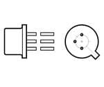
2N4391 2N4392 2N4393 SILICON N-CHANNEL JFET ELECTRICAL CHARACTERISTICS - Continued: (TA=25°C unless otherwise noted) 2N4391 2N4392 2N4393 SYMBOL TEST CONDITIONS MIN MAX MIN MAX MIN MAX UNITS tr ID(ON)=12mA - 5.0 - - - - ns tr ID(ON)=6.0mA - - - 5.0 - - ns tr ID(ON)=3.0mA - - - - - 5.0 ns tf VGS(OFF)=12V - 15 - - - - ns tf VGS(OFF)=7.0V - - - 20 - - ns tf VGS(OFF)=5.0V - - - - - 30 ns ton ID(ON)=12mA - 15 - - - - ns ton ID(ON)=6.0mA - - - 15 - - ns ton ID(ON)=3.0mA - - - - - 15 ns toff VGS(OFF)=12V - 20 - - - - ns toff VGS(OFF)=7.0V - - - 35 - - ns toff VGS(OFF)=5.0V - - - - - 50 ns TO-18 CASE - MECHANICAL OUTLINE LEAD CODE: 1) Source 2) Drain 3) Gate MARKING: FULL PART NUMBER R2 (26-September 2016) www.centralsemi.com
2N4391 2N4392 2N4393 SILICON N-CHANNEL JFET TYPICAL ELECTRICAL CHARACTERISTICS R2 (26-September 2016) www.centralsemi.com
OUTSTANDING SUPPORT AND SUPERIOR SERVICES PRODUCT SUPPORT Central’s operations team provides the highest level of support to insure product is delivered on-time. • Supply management (Customer portals) • Custom bar coding for shipments • Inventory bonding • Custom product packing • Consolidated shipping options DESIGNER SUPPORT/SERVICES Central’s applications engineering team is ready to discuss your design challenges. Just ask. • Free quick ship samples (2nd day air) • Special wafer diffusions • Online technical data and parametric search • PbSn plating options • SPICE models • Package details • Custom electrical curves • Application notes • Environmental regulation compliance • Application and design sample kits • Customer specific screening • Custom product and package development • Up-screening capabilities REQUESTING PRODUCT PLATING 1. If requesting Tin/Lead plated devices, add the suffix “ TIN/LEAD” to the part number when ordering (example: 2N2222A TIN/LEAD). 2. If requesting Lead (Pb) Free plated devices, add the suffix “ PBFREE” to the part number when ordering (example: 2N2222A PBFREE). CONTACT US Corporate Headquarters & Customer Support Team Central Semiconductor Corp. 145 Adams Avenue Worldwide Field Representatives: Hauppauge, NY 11788 USA www.centralsemi.com/wwreps Main Tel: (631) 435-1110 Main Fax: (631) 435-1824 Worldwide Distributors: Support Team Fax: (631) 435-3388 www.centralsemi.com/wwdistributors www.centralsemi.com For the latest version of Central Semiconductor’s LIMITATIONS AND DAMAGES DISCLAIMER, which is part of Central’s Standard Terms and Conditions of sale, visit: www.centralsemi.com/terms www.centralsemi.com (001)
Mouser Electronics Authorized Distributor Click to View Pricing, Inventory, Delivery & Lifecycle Information: C entral Semiconductor: 2N4391 2N4392 2N4393