ICGOO在线商城 > 25LC080/P

 Datasheet下载
- 型号: 25LC080/P
- 制造商: Microchip
- 库位|库存: xxxx|xxxx
- 要求:
| 数量阶梯 | 香港交货 | 国内含税 |
| +xxxx | $xxxx | ¥xxxx |
查看当月历史价格
查看今年历史价格
25LC080/P产品简介:
ICGOO电子元器件商城为您提供25LC080/P由Microchip设计生产,在icgoo商城现货销售,并且可以通过原厂、代理商等渠道进行代购。 提供25LC080/P价格参考以及Microchip25LC080/P封装/规格参数等产品信息。 你可以下载25LC080/P参考资料、Datasheet数据手册功能说明书, 资料中有25LC080/P详细功能的应用电路图电压和使用方法及教程。
| 参数 | 数值 |
| 产品目录 | 集成电路 (IC) |
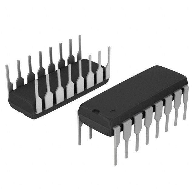
| 描述 | IC EEPROM 8KBIT 2MHZ 8DIP |
| 产品分类 | |
| 品牌 | Microchip Technology |
| 数据手册 | http://www.microchip.com/mymicrochip/filehandler.aspx?ddocname=en011221http://www.microchip.com/mymicrochip/filehandler.aspx?ddocname=en539525 |
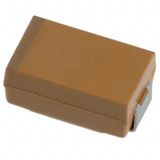
| 产品图片 |
|
| 产品型号 | 25LC080/P |
| rohs | 无铅 / 符合限制有害物质指令(RoHS)规范要求 |
| 产品系列 | - |
| 产品目录页面 | |
| 供应商器件封装 | 8-PDIP |
| 包装 | 管件 |
| 存储器类型 | EEPROM |
| 存储容量 | 8K (1K x 8) |
| 封装/外壳 | 8-DIP(0.300",7.62mm) |
| 工作温度 | 0°C ~ 70°C |
| 接口 | SPI 串行 |
| 标准包装 | 60 |
| 格式-存储器 | EEPROMs - 串行 |
| 电压-电源 | 2.5 V ~ 5.5 V |
| 速度 | 2MHz |


- 商务部:美国ITC正式对集成电路等产品启动337调查
- 曝三星4nm工艺存在良率问题 高通将骁龙8 Gen1或转产台积电
- 太阳诱电将投资9.5亿元在常州建新厂生产MLCC 预计2023年完工
- 英特尔发布欧洲新工厂建设计划 深化IDM 2.0 战略
- 台积电先进制程称霸业界 有大客户加持明年业绩稳了
- 达到5530亿美元!SIA预计今年全球半导体销售额将创下新高
- 英特尔拟将自动驾驶子公司Mobileye上市 估值或超500亿美元
- 三星加码芯片和SET,合并消费电子和移动部门,撤换高东真等 CEO
- 三星电子宣布重大人事变动 还合并消费电子和移动部门
- 海关总署:前11个月进口集成电路产品价值2.52万亿元 增长14.8%


PDF Datasheet 数据手册内容提取
Not recommended for new designs – Please use 25AA080A/B or 25LC080A/B. 25AA080/25LC080/25C080 8K SPI Bus Serial EEPROM Device Selection Table Description: The Microchip Technology Inc. 25AA080/25LC080/ Part VCC Max. Clock Temp. 25C080 (25XX080*) are 8 Kbit Serial Electrically Number Range Frequency Ranges Erasable PROMs. The memory is accessed via a 25AA080 1.8-5.5V 1MHz I simple Serial Peripheral Interface (SPI) compatible 25LC080 2.5-5.5V 2MHz I serial bus. The bus signals required are a clock input (SCK) plus separate data in (SI) and data out (SO) 25C080 4.5-5.5V 3MHz I,E lines. Access to the device is controlled through a Chip Select (CS) input. Features: Communication to the device can be paused via the • Low-power CMOS technology: hold pin (HOLD). While the device is paused, transi- - Write current: 3mA maximum tions on its inputs will be ignored, with the exception of - Read current: 500A typical chip select, allowing the host to service higher priority interrupts. - Standby current: 500nA typical • 1024 x 8-bit organization Package Types • 16 byte page • Write cycle time: 5 ms max. PDIP/SOIC • Self-timed erase and write cycles CS 1 8 VCC • Block write protection: 2 SO 2 5 7 HOLD - Protect none, 1/4, 1/2 or all of array A A • Built-in write protection: WP 3 0 6 SCK 8 0 - Power-on/off data protection circuitry VSS 4 / 5 SI - Write enable latch - Write-protect pin • Sequential read Block Diagram • High reliability: Status - Endurance: 1M cycles HV Generator Register - Data retention: > 200 years - ESD protection: > 4000V • 8-pin PDIP and SOIC (150 mil) • Temperature ranges supported: EEPROM - Industrial (I): -40C to +85C I/O Control Memory X Array - Automotive (E) (25C080): -40°C to +125°C Logic Control Logic Dec Page Latches SI SO Y Decoder CS SCK Sense Amp. HOLD R/W Control WP VCC VSS 1997-2012 Microchip Technology Inc. DS21230E-page 1
25AA080/25LC080/25C080 1.0 ELECTRICAL CHARACTERISTICS Absolute Maximum Ratings(†) VCC.............................................................................................................................................................................7.0V All inputs and outputs w.r.t. VSS........................................................................................................-0.6V to VCC + 1.0V Storage temperature.................................................................................................................................-65°C to 150°C Ambient temperature under bias...............................................................................................................-40°C to 125°C Soldering temperature of leads (10 seconds).......................................................................................................+300°C ESD protection on all pins.........................................................................................................................................4KV † NOTICE: Stresses above those listed under ‘Maximum ratings’ may cause permanent damage to the device. This is a stress rating only and functional operation of the device at those or any other conditions above those indicated in the operational listings of this specification is not implied. Exposure to maximum rating conditions for an extended period of time may affect device reliability. 1.1 DC Characteristics Industrial (I): TA = -40°C to +85°C VCC = 1.8V to 5.5V DC CHARACTERISTICS Automotive (E):TA = -40°C to +125°C VCC = 4.5V to 5.5V (25C080 only) Param. Sym. Characteristic Min. Max. Units Test Conditions No. D001 VIH1 High-level input 2.0 VCC+1 V VCC2.7V (Note) voltage D002 VIH2 0.7 VCC VCC+1 V VCC< 2.7V (Note) D003 VIL1 Low-level input -0.3 0.8 V VCC2.7V (Note) D004 VIL2 voltage -0.3 0.3 VCC V VCC < 2.7V (Note) D005 VOL Low-level output — 0.4 V IOL = 2.1mA D006 VOL voltage — 0.2 V IOL = 1.0mA, VCC < 2.5V D007 VOH High-level output VCC -0.5 — V IOH = -400A voltage D008 ILI Input leakage current -10 10 A CS = VCC, VIN = VSS TO VCC D009 ILO Output leakage -10 10 A CS = VCC, VOUT = VSS TO VCC current D010 CINT Internal Capacitance — 7 pF TA = 25°C, CLK = 1.0MHz, (all inputs and VCC = 5.0V (Note) outputs) D011 ICC Read — 1 mA VCC = 5.5V; FCLK = 3.0MHz; — 500 A SO = Open Operating Current VCC = 2.5V; FCLK = 2.0MHz; SO = Open D012 ICC Write — 5 mA VCC = 5.5V — 3 mA VCC = 2.5V D013 ICCS — 5 A CS = VCC = 5.5V, Inputs tied to VCC or Standby Current — 1 A VSS CS = VCC = 2.5V, Inputs tied to VCC or VSS Note: This parameter is periodically sampled and not 100% tested. DS21230E-page 2 1997-2012 Microchip Technology Inc.
25AA080/25LC080/25C080 1.2 AC Characteristics Industrial (I): TA = -40°C to +85°C VCC = 1.8V to 5.5V AC CHARACTERISTICS Automotive (E): TA = -40°C to +125°C VCC = 4.5V to 5.5V (25C080 only) Param. Sym. Characteristic Min. Max. Units Test Conditions No. 1 FCLK Clock Frequency — 3 MHz VCC = 4.5V to 5.5V — 2 MHz VCC = 2.5V to 4.5V — 1 MHz VCC = 1.8V to 2.5V 2 TCSS CS Setup Time 100 — ns VCC = 4.5V to 5.5V 250 — ns VCC = 2.5V to 4.5V 500 — ns VCC = 1.8V to 2.5V 3 TCSH CS Hold Time 150 — ns VCC = 4.5V to 5.5V 250 — ns VCC = 2.5V to 4.5V 475 — ns VCC = 1.8V to 2.5V 4 TCSD CS Disable Time 500 — ns — 5 Tsu Data Setup Time 30 — ns VCC = 4.5V to 5.5V 50 — ns VCC = 2.5V to 4.5V 50 — ns VCC = 1.8V to 2.5V 6 THD Data Hold Time 50 — ns VCC = 4.5V to 5.5V 100 — ns VCC = 2.5V to 4.5V 100 — ns VCC = 1.8V to 2.5V 7 TR CLK Rise Time — 2 s (Note1) 8 TF CLK Fall Time — 2 s (Note1) 9 THI Clock High Time 150 — ns VCC = 4.5V to 5.5V 230 — ns VCC = 2.5V to 4.5V 475 — ns VCC = 1.8V to 2.5V 10 TLO Clock Low Time 150 — ns VCC = 4.5V to 5.5V 230 — ns VCC = 2.5V to 4.5V 475 — ns VCC = 1.8V to 2.5V 11 TCLD Clock Delay Time 50 — ns — 12 TCLE Clock Enable Time 50 — ns — 13 TV Output Valid from Clock Low — 150 ns VCC = 4.5V to 5.5V — 230 ns VCC = 2.5V to 4.5V — 475 ns VCC = 1.8V to 2.5V 14 THO Output Hold Time 0 — ns (Note1) 15 TDIS Output Disable Time — 200 ns VCC = 4.5V to 5.5V (Note1) — 250 ns VCC = 2.5V to 4.5V (Note1) — 500 ns VCC = 1.8V to 2.5V (Note1) 16 THS HOLD Setup Time 100 — ns VCC = 4.5V to 5.5V 100 — ns VCC = 2.5V to 4.5V 200 — ns VCC = 1.8V to 2.5V 17 THH HOLD Hold Time 100 — ns VCC = 4.5V to 5.5V 100 — ns VCC = 2.5V to 4.5V 200 — ns VCC = 1.8V to 2.5V 18 THZ HOLD Low to Output High-Z 100 — ns VCC = 4.5V to 5.5V (Note1) 150 — ns VCC = 2.5V to 4.5V (Note1) 200 — ns VCC = 1.8V to 2.5V (Note1) 19 THV HOLD High to Output Valid 100 — ns VCC = 4.5V to 5.5V 150 — ns VCC = 2.5V to 4.5V 200 — ns VCC = 1.8V to 2.5V 20 TWC Internal Write Cycle Time — 5 ms — 21 — Endurance 1M — E/W (Note2) Cycles Note 1: This parameter is periodically sampled and not 100% tested. 2: This parameter is not tested but ensured by characterization. For endurance estimates in a specific application, please consult the Total Endurance™ Model which can be obtained from Microchip’s web site at: www.microchip.com. 1997-2012 Microchip Technology Inc. DS21230E-page 3
25AA080/25LC080/25C080 FIGURE 1-1: HOLD TIMING CS 17 17 16 16 SCK 18 19 High-impedance SO n+2 n+1 n n n-1 don’t care 5 SI n+2 n+1 n n n-1 HOLD FIGURE 1-2: SERIAL INPUT TIMING 4 CS 12 2 11 7 Mode 1,1 8 3 SCK Mode 0,0 5 6 SI MSB in LSB in High-impedance SO FIGURE 1-3: SERIAL OUTPUT TIMING CS 9 10 3 Mode 1,1 SCK Mode 0,0 13 15 14 SO MSB out ISB out don’t care SI DS21230E-page 4 1997-2012 Microchip Technology Inc.
25AA080/25LC080/25C080 1.3 AC Test Conditions FIGURE 1-4: AC TEST CIRCUIT AC Waveform: VCC VLO = 0.2V — VHI = VCC - 0.2V (Note 1) 2.25 K VHI = 4.0V (Note 2) Timing Measurement Reference Level SO Input 0.5 VCC 1.8 K 100pF Output 0.5 VCC Note1: For VCC 4.0V 2: For VCC > 4.0V 1997-2012 Microchip Technology Inc. DS21230E-page 5
25AA080/25LC080/25C080 2.0 PIN DESCRIPTIONS 2.4 Serial Input (SI) The descriptions of the pins are listed in Table2-1. The SI pin is used to transfer data into the device. It receives instructions, addresses and data. Data is TABLE 2-1: PIN FUNCTION TABLE latched on the rising edge of the serial clock. Name PDIP SOIC Function 2.5 Serial Clock (SCK) CS 1 1 Chip Select Input The SCK is used to synchronize the communication SO 2 2 Serial Data Output between a master and the 25XX080. Instructions, WP 3 3 Write-Protect Pin addresses or data present on the SI pin are latched on the rising edge of the clock input, while data on the SO Vss 4 4 Ground pin is updated after the falling edge of the clock input. SI 5 5 Serial Data Input SCK 6 6 Serial Clock Input 2.6 Hold (HOLD) HOLD 7 7 Hold Input The HOLD pin is used to suspend transmission to the Vcc 8 8 Supply Voltage 25XX080 while in the middle of a serial sequence without having to retransmit the entire sequence again. 2.1 Chip Select (CS) It must be held high any time this function is not being used. Once the device is selected and a serial A low level on this pin selects the device. A high level sequence is underway, the HOLD pin may be pulled deselects the device and forces it into Standby mode. low to pause further serial communication without However, a programming cycle which is already resetting the serial sequence. The HOLD pin must be initiated or in progress will be completed, regardless of brought low while SCK is low, otherwise the HOLD the CS input signal. If CS is brought high during a function will not be invoked until the next SCK high-to- program cycle, the device will go into Standby mode as low transition. The 25XX080 must remain selected soon as the programming cycle is complete. When the during this sequence. The SI, SCK and SO pins are in device is deselected, SO goes to the high-impedance a high-impedance state during the time the device is state, allowing multiple parts to share the same SPI paused and transitions on these pins will be ignored. To bus. A low-to-high transition on CS after a valid write resume serial communication, HOLD must be brought sequence initiates an internal write cycle. After power- high while the SCK pin is low, otherwise serial commu- up, a low level on CS is required prior to any sequence nication will not resume. Lowering the HOLD line at any being initiated. time will tri-state the SO line. 2.2 Serial Output (SO) The SO pin is used to transfer data out of the 25XX080. During a read cycle, data is shifted out on this pin after the falling edge of the serial clock. 2.3 Write-Protect (WP) This pin is used in conjunction with the WPEN bit in the Status register to prohibit writes to the nonvolatile bits in the Status register. When WP is low and WPEN is high, writing to the nonvolatile bits in the Status register is disabled. All other operations function normally. When WP is high, all functions, including writes to the nonvolatile bits in the Status register operate normally. If the WPEN bit is set, WP low during a Status register write sequence will disable writing to the Status register. If an internal write cycle has already begun, WP going low will have no effect on the write. The WP pin function is blocked when the WPEN bit in the Status register is low. This allows the user to install the 25XX080 in a system with WP pin grounded and still be able to write to the Status register. The WP pin functions will be enabled when the WPEN bit is set high. DS21230E-page 6 1997-2012 Microchip Technology Inc.
25AA080/25LC080/25C080 3.0 FUNCTIONAL DESCRIPTION 3.3 Write Sequence Prior to any attempt to write data to the 25XX080, the 3.1 Principles of Operation write enable latch must be set by issuing the WREN instruction (Figure3-4). This is done by setting CS low The 25XX080 are 1024 byte Serial EEPROMs and then clocking out the proper instruction into the designed to interface directly with the Serial Peripheral 25XX080. After all eight bits of the instruction are trans- Interface (SPI) port of many of today’s popular micro- mitted, the CS must be brought high to set the write controller families, including Microchip’s PIC16C6X/7X enable latch. If the write operation is initiated immedi- microcontrollers. It may also interface with microcon- ately after the WREN instruction without CS being trollers that do not have a built-in SPI port by using brought high, the data will not be written to the array discrete I/O lines programmed properly with the because the write enable latch will not have been software. properly set. The 25XX080 contains an 8-bit instruction register. The Once the write enable latch is set, the user may device is accessed via the SI pin, with data being proceed by setting the CS low, issuing a WRITE instruc- clocked in on the rising edge of SCK. The CS pin must tion, followed by the 16-bit address, with the six MSBs be low and the HOLD pin must be high for the entire of the address being “don’t care” bits, and then the data operation. The WP pin must be held high to allow to be written. Up to 16 bytes of data can be sent to the writing to the memory array. 25XX080 before a write cycle is necessary. The only Table3-1 contains a list of the possible instruction restriction is that all of the bytes must reside in the bytes and format for device operation. All instructions, same page. A page address begins with xxxx xxxx addresses, and data are transferred MSB first, LSB xxxx 0000 and ends with xxxx xxxx xxxx 1111. last. If the internal address counter reaches xxxx xxxx Data is sampled on the first rising edge of SCK after CS xxxx 1111 and the clock continues, the counter will goes low. If the clock line is shared with other periph- roll back to the first address of the page and overwrite eral devices on the SPI bus, the user can assert the any data in the page that may have been written. HOLD input and place the 25XX080 in ‘HOLD’ mode. For the data to be actually written to the array, the CS After releasing the HOLD pin, operation will resume must be brought high after the Least Significant bit (D0) from the point when the HOLD was asserted. of the nth data byte has been clocked in. If CS is brought high at any other time, the write operation will 3.2 Read Sequence not be completed. Refer to Figure3-2 and Figure3-3 for more detailed illustrations on the byte write The device is selected by pulling CS low. The 8-bit READ sequence and the page write sequence respectively. instruction is transmitted to the 25XX080 followed by While the write is in progress, the Status register may the 16-bit address, with the six MSBs of the address be read to check the status of the WPEN, WIP, WEL, being "don’t care" bits. After the correct READ instruction BP1 and BP0 bits (Figure3-6). A read attempt of a and address are sent, the data stored in the memory at memory array location will not be possible during a the selected address is shifted out on the SO pin. The write cycle. When the write cycle is completed, the data stored in the memory at the next address can be write enable latch is reset. read sequentially by continuing to provide clock pulses. The internal address pointer is automatically incre- mented to the next higher address after each byte of data is shifted out. When the highest address is reached (03FFh), the address counter rolls over to address 0000h allowing the read cycle to be continued indefi- nitely. The read operation is terminated by raising the CS pin (Figure3-1). TABLE 3-1: INSTRUCTION SET Instruction Name Instruction Format Description READ 0000 0011 Read data from memory array beginning at selected address WRITE 0000 0010 Write data to memory array beginning at selected address WRDI 0000 0100 Reset the write enable latch (disable write operations) WREN 0000 0110 Set the write enable latch (enable write operations) RDSR 0000 0101 Read Status register WRSR 0000 0001 Write Status register 1997-2012 Microchip Technology Inc. DS21230E-page 7
25AA080/25LC080/25C080 FIGURE 3-1: READ SEQUENCE CS 0 1 2 3 4 5 6 7 8 9 10 11 21 22 23 24 25 26 27 28 29 30 31 SCK instruction 16-bit address SI 0 0 0 0 0 0 1 1 15 14 13 12 2 1 0 data out High-impedance SO 7 6 5 4 3 2 1 0 FIGURE 3-2: BYTE WRITE SEQUENCE CS Twc 0 1 2 3 4 5 6 7 8 9 10 11 21 22 23 24 25 26 27 28 29 30 31 SCK instruction 16-bit address data byte SI 0 0 0 0 0 0 1 0 15 14 13 12 2 1 0 7 6 5 4 3 2 1 0 High-impedance SO FIGURE 3-3: PAGE WRITE SEQUENCE CS 0 1 2 3 4 5 6 7 8 9 10 11 21 22 23 24 25 26 27 28 29 30 31 SCK instruction 16-bit address data byte 1 SI 0 0 0 0 0 0 1 0 15 14 13 12 2 1 0 7 6 5 4 3 2 1 0 CS 32 33 34 35 36 37 38 39 40 41 42 43 44 45 46 47 SCK data byte 2 data byte 3 data byte n (16 max) SI 7 6 5 4 3 2 1 0 7 6 5 4 3 2 1 0 7 6 5 4 3 2 1 0 DS21230E-page 8 1997-2012 Microchip Technology Inc.
25AA080/25LC080/25C080 3.4 Write Enable (WREN) and Write The following is a list of conditions under which the Disable (WRDI) write enable latch will be reset: • Power-up The 25XX080 contains a write enable latch. See • WRDI instruction successfully executed Table3-3 for the Write-Protect Functionality Matrix. This latch must be set before any write operation will be • WRSR instruction successfully executed completed internally. The WREN instruction will set the • WRITE instruction successfully executed latch, and the WRDI will reset the latch. FIGURE 3-4: WRITE ENABLE SEQUENCE CS 0 1 2 3 4 5 6 7 SCK 0 0 0 0 0 1 1 0 SI High-impedance SO FIGURE 3-5: WRITE DISABLE SEQUENCE CS 0 1 2 3 4 5 6 7 SCK 0 0 0 0 0 1 10 0 SI High-impedance SO 1997-2012 Microchip Technology Inc. DS21230E-page 9
25AA080/25LC080/25C080 3.5 Read Status Register (RDSR) The Write Enable Latch (WEL) bit indicates the status of the write enable latch. When set to a ‘1’, the latch The Read Status Register (RDSR) instruction provides allows writes to the array, when set to a ‘0’, the latch access to the Status register. The Status register may prohibits writes to the array. The state of this bit can be read at any time, even during a write cycle. The always be updated via the WREN or WRDI commands Status register is formatted as follows: regardless of the state of write protection on the Status 7 6 5 4 3 2 1 0 register. This bit is read only. WPEN X X X BP1 BP0 WEL WIP The Block Protection (BP0 and BP1) bits indicate which blocks are currently write-protected. These bits The Write-In-Process (WIP) bit indicates whether the are set by the user issuing the WRSR instruction. These 25XX080 is busy with a write operation. When set to a bits are nonvolatile. ‘1’, a write is in progress, when set to a ‘0’, no write is in progress. This bit is read-only. See Figure3-6 for the RDSR timing sequence. FIGURE 3-6: READ STATUS REGISTER TIMING SEQUENCE CS 0 1 2 3 4 5 6 7 8 9 10 11 12 13 14 15 SCK instruction SI 0 0 0 0 0 1 0 1 data from Status register High-impedance SO 7 6 5 4 3 2 1 0 DS21230E-page 10 1997-2012 Microchip Technology Inc.
25AA080/25LC080/25C080 3.6 Write Status Register (WRSR) TABLE 3-2: ARRAY PROTECTION The Write Status Register (WRSR) instruction allows the Array Addresses BP1 BP0 user to select one of four levels of protection for the Write-Protected array by writing to the appropriate bits in the Status reg- 0 0 none ister. The array is divided up into four segments. The 0 1 upper 1/4 user has the ability to write-protect none, one, two, or (0300h - 03FFh) all four of the segments of the array. The partitioning is controlled as shown in Table3-2. 1 0 upper 1/2 (0200h - 03FFh) The Write-Protect Enable (WPEN) bit is a nonvolatile bit that is available as an enable bit for the WP pin. The 1 1 all Write-Protect (WP) pin and the Write-Protect Enable (0000h - 03FFh) (WPEN) bit in the Status register control the program- mable hardware write-protect feature. Hardware write protection is enabled when WP pin is low and the WPEN bit is high. Hardware write protection is disabled when either the WP pin is high or the WPEN bit is low. When the chip is hardware write-protected, only writes to nonvolatile bits in the Status register are disabled. See Table 3-3 for a matrix of functionality on the WPEN bit. See Figure3-5 for the WRSR timing sequence. FIGURE 3-7: WRITE STATUS REGISTER TIMING SEQUENCE CS 0 1 2 3 4 5 6 7 8 9 10 11 12 13 14 15 SCK instruction data to Status register SI 0 0 0 0 0 0 0 1 7 6 5 4 3 2 1 0 High-impedance SO 1997-2012 Microchip Technology Inc. DS21230E-page 11
25AA080/25LC080/25C080 3.7 Data Protection 3.8 Power-On State The following protection has been implemented to The 25XX080 powers on in the following state: prevent inadvertent writes to the array: • The device is in low-power Standby mode • The write enable latch is reset on power-up (CS=1) • A WRITE ENABLE instruction must be issued to • The write enable latch is reset set the write enable latch • SO is in high-impedance state • After a byte write, page write or Status register • A high-to-low level transition on CS is required to write, the write enable latch is reset enter active state • CS must be set high after the proper number of clock cycles to start an internal write cycle • Access to the array during an internal write cycle is ignored and programming is continued TABLE 3-3: WRITE-PROTECT FUNCTIONALITY MATRIX WPEN WP WEL Protected Blocks Unprotected Blocks Status Register X X 0 Protected Protected Protected 0 X 1 Protected Writable Writable 1 Low 1 Protected Writable Protected X High 1 Protected Writable Writable DS21230E-page 12 1997-2012 Microchip Technology Inc.
25AA080/25LC080/25C080 4.0 PACKAGING INFORMATION 4.1 Package Marking Information 8-Lead PDIP (300 mil) Example: XXXXXXXX 25LC080 XXXXXNNN /PNNN YYWW YYWW 8-Lead SOIC (150 mil) Example: XXXXXXXX 25LC080 XXXXYYWW /SNYYWW NNN NNN Legend: XX...X Customer specific information* Y Year code (last digit of calendar year) YY Year code (last 2 digits of calendar year) WW Week code (week of January 1 is week ‘01’) NNN Alphanumeric traceability code Note: In the event the full Microchip part number cannot be marked on one line, it will be carried over to the next line thus limiting the number of available characters for customer specific information. 1997-2012 Microchip Technology Inc. DS21230E-page 13
25AA080/25LC080/25C080 8-Lead Plastic Dual In-line (P) – 300 mil (PDIP) Note: For the most current package drawings, please see the Microchip Packaging Specification located at http://www.microchip.com/packaging E1 D 2 n 1 E A A2 L c A1 B1 p eB B Units INCHES* MILLIMETERS Dimension Limits MIN NOM MAX MIN NOM MAX Number of Pins n 8 8 Pitch p .100 2.54 Top to Seating Plane A .140 .155 .170 3.56 3.94 4.32 Molded Package Thickness A2 .115 .130 .145 2.92 3.30 3.68 Base to Seating Plane A1 .015 0.38 Shoulder to Shoulder Width E .300 .313 .325 7.62 7.94 8.26 Molded Package Width E1 .240 .250 .260 6.10 6.35 6.60 Overall Length D .360 .373 .385 9.14 9.46 9.78 Tip to Seating Plane L .125 .130 .135 3.18 3.30 3.43 Lead Thickness c .008 .012 .015 0.20 0.29 0.38 Upper Lead Width B1 .045 .058 .070 1.14 1.46 1.78 Lower Lead Width B .014 .018 .022 0.36 0.46 0.56 Overall Row Spacing § eB .310 .370 .430 7.87 9.40 10.92 Mold Draft Angle Top 5 10 15 5 10 15 Mold Draft Angle Bottom 5 10 15 5 10 15 * Controlling Parameter § Significant Characteristic Notes: Dimensions D and E1 do not include mold flash or protrusions. Mold flash or protrusions shall not exceed .010” (0.254mm) per side. JEDEC Equivalent: MS-001 Drawing No. C04-018 DS21230E-page 14 1997-2012 Microchip Technology Inc.
25AA080/25LC080/25C080 8-Lead Plastic Small Outline (SN) – Narrow, 150 mil (SOIC) Note: For the most current package drawings, please see the Microchip Packaging Specification located at http://www.microchip.com/packaging E E1 p D 2 B n 1 h 45× c A A2 f L A1 Units INCHES* MILLIMETERS Dimension Limits MIN NOM MAX MIN NOM MAX Number of Pins n 8 8 Pitch p .050 1.27 Overall Height A .053 .061 .069 1.35 1.55 1.75 Molded Package Thickness A2 .052 .056 .061 1.32 1.42 1.55 Standoff § A1 .004 .007 .010 0.10 0.18 0.25 Overall Width E .228 .237 .244 5.79 6.02 6.20 Molded Package Width E1 .146 .154 .157 3.71 3.91 3.99 Overall Length D .189 .193 .197 4.80 4.90 5.00 Chamfer Distance h .010 .015 .020 0.25 0.38 0.51 Foot Length L .019 .025 .030 0.48 0.62 0.76 Foot Angle f 0 4 8 0 4 8 Lead Thickness c .008 .009 .010 0.20 0.23 0.25 Lead Width B .013 .017 .020 0.33 0.42 0.51 Mold Draft Angle Top 0 12 15 0 12 15 Mold Draft Angle Bottom 0 12 15 0 12 15 * Controlling Parameter § Significant Characteristic Notes: Dimensions D and E1 do not include mold flash or protrusions. Mold flash or protrusions shall not exceed .010” (0.254mm) per side. JEDEC Equivalent: MS-012 Drawing No. C04-057 1997-2012 Microchip Technology Inc. DS21230E-page 15
25AA080/25LC080/25C080 APPENDIX A: REVISION HISTORY Revision D Added note to page 1 header (Not recommended for new designs). Updated document format. Revision E Added a note to each package outline drawing. DS21230E-page 16 1997-2012 Microchip Technology Inc.
25AA080/25LC080/25C080 THE MICROCHIP WEB SITE CUSTOMER SUPPORT Microchip provides online support via our WWW site at Users of Microchip products can receive assistance www.microchip.com. This web site is used as a means through several channels: to make files and information easily available to • Distributor or Representative customers. Accessible by using your favorite Internet • Local Sales Office browser, the web site contains the following • Field Application Engineer (FAE) information: • Technical Support • Product Support – Data sheets and errata, application notes and sample programs, design Customers should contact their distributor, resources, user’s guides and hardware support representative or field application engineer (FAE) for documents, latest software releases and archived support. Local sales offices are also available to help software customers. A listing of sales offices and locations is included in the back of this document. • General Technical Support – Frequently Asked Questions (FAQ), technical support requests, Technical support is available through the web site online discussion groups, Microchip consultant at: http://microchip.com/support program member listing • Business of Microchip – Product selector and ordering guides, latest Microchip press releases, listing of seminars and events, listings of Microchip sales offices, distributors and factory representatives CUSTOMER CHANGE NOTIFICATION SERVICE Microchip’s customer notification service helps keep customers current on Microchip products. Subscribers will receive e-mail notification whenever there are changes, updates, revisions or errata related to a specified product family or development tool of interest. To register, access the Microchip web site at www.microchip.com. Under “Support”, click on “Customer Change Notification” and follow the registration instructions. 1997-2012 Microchip Technology Inc. DS21230E-page 17
25AA080/25LC080/25C080 READER RESPONSE It is our intention to provide you with the best documentation possible to ensure successful use of your Microchip product. If you wish to provide your comments on organization, clarity, subject matter, and ways in which our documentation can better serve you, please FAX your comments to the Technical Publications Manager at (480)792-4150. Please list the following information, and use this outline to provide us with your comments about this document. TO: Technical Publications Manager Total Pages Sent ________ RE: Reader Response From: Name Company Address City / State / ZIP / Country Telephone: (_______) _________ - _________ FAX: (______) _________ - _________ Application (optional): Would you like a reply? Y N Device: 25AA080/25LC080/25C080 Literature Number: DS21230E Questions: 1. What are the best features of this document? 2. How does this document meet your hardware and software development needs? 3. Do you find the organization of this document easy to follow? If not, why? 4. What additions to the document do you think would enhance the structure and subject? 5. What deletions from the document could be made without affecting the overall usefulness? 6. Is there any incorrect or misleading information (what and where)? 7. How would you improve this document? DS21230E-page 18 1997-2012 Microchip Technology Inc.
25AA080/25LC080/25C080 PRODUCT IDENTIFICATION SYSTEM To order or obtain information, e.g., on pricing or delivery, refer to the factory or the listed sales office. PART NO. X /XX XXX Examples: Device Temperature Package Pattern a) 25AA080-I/SN: Industrial Temp., Range SOIC package b) 25AA080T-I/SN: Tape and Reel, Industrial Temp., SOIC package Device 25AA080: 8 Kbit 1.8V SPI Serial EEPROM c) 25LC080-I/SN: Industrial Temp., 25AA080T: 8 Kbit 1.8V SPI Serial EEPROM SOIC package (Tape and Reel) 25LC080: 8 Kbit 2.5V SPI Serial EEPROM d) 25LC080T-I/SN: Tape and Reel, 25LC080: 8 Kbit 2.5V SPI Serial EEPROM Industrial Temp., SOIC package (Tape and Reel) e) 25C080-I/P: Industrial Temp., 25C080: 8 Kbit 5.0V SPI Serial EEPROM PDIP package 25C080: 8 Kbit 5.0V SPI Serial EEPROM f) 25C080-I/SN: Industrial Temp., (Tape and Reel) SOIC package g) 25C080T-I/SN: Tape and Reel, Industrial Temp., SOIC package Temperature I = -40C to +85C h) 25C080-E/SN: Extended Temp., Range E = -40C to+125C SOIC package Package P = Plastic DIP (300 mil body), 8-lead SN = Plastic SOIC (150 mil body), 8-lead Sales and Support Data Sheets Products supported by a preliminary Data Sheet may have an errata sheet describing minor operational differences and recommended workarounds. To determine if an errata sheet exists for a particular device, please contact one of the following: 1. Your local Microchip sales office 2. The Microchip Worldwide Site (www.microchip.com) Please specify which device, revision of silicon and Data Sheet (include Literature #) you are using. New Customer Notification System Register on our web site (www.microchip.com/cn) to receive the most current information on our products. 1997-2012 Microchip Technology Inc. DS21230E-page 19
25AA080/25LC080/25C080 NOTES: DS21230E-page 20 1997-2012 Microchip Technology Inc.
Note the following details of the code protection feature on Microchip devices: • Microchip products meet the specification contained in their particular Microchip Data Sheet. • Microchip believes that its family of products is one of the most secure families of its kind on the market today, when used in the intended manner and under normal conditions. • There are dishonest and possibly illegal methods used to breach the code protection feature. All of these methods, to our knowledge, require using the Microchip products in a manner outside the operating specifications contained in Microchip’s Data Sheets. Most likely, the person doing so is engaged in theft of intellectual property. • Microchip is willing to work with the customer who is concerned about the integrity of their code. • Neither Microchip nor any other semiconductor manufacturer can guarantee the security of their code. Code protection does not mean that we are guaranteeing the product as “unbreakable.” Code protection is constantly evolving. We at Microchip are committed to continuously improving the code protection features of our products. Attempts to break Microchip’s code protection feature may be a violation of the Digital Millennium Copyright Act. If such acts allow unauthorized access to your software or other copyrighted work, you may have a right to sue for relief under that Act. Information contained in this publication regarding device Trademarks applications and the like is provided only for your convenience The Microchip name and logo, the Microchip logo, dsPIC, and may be superseded by updates. It is your responsibility to FlashFlex, KEELOQ, KEELOQ logo, MPLAB, PIC, PICmicro, ensure that your application meets with your specifications. PICSTART, PIC32 logo, rfPIC, SST, SST Logo, SuperFlash MICROCHIP MAKES NO REPRESENTATIONS OR and UNI/O are registered trademarks of Microchip Technology WARRANTIES OF ANY KIND WHETHER EXPRESS OR Incorporated in the U.S.A. and other countries. IMPLIED, WRITTEN OR ORAL, STATUTORY OR OTHERWISE, RELATED TO THE INFORMATION, FilterLab, Hampshire, HI-TECH C, Linear Active Thermistor, INCLUDING BUT NOT LIMITED TO ITS CONDITION, MTP, SEEVAL and The Embedded Control Solutions QUALITY, PERFORMANCE, MERCHANTABILITY OR Company are registered trademarks of Microchip Technology FITNESS FOR PURPOSE. Microchip disclaims all liability Incorporated in the U.S.A. arising from this information and its use. Use of Microchip Silicon Storage Technology is a registered trademark of devices in life support and/or safety applications is entirely at Microchip Technology Inc. in other countries. the buyer’s risk, and the buyer agrees to defend, indemnify and Analog-for-the-Digital Age, Application Maestro, BodyCom, hold harmless Microchip from any and all damages, claims, chipKIT, chipKIT logo, CodeGuard, dsPICDEM, suits, or expenses resulting from such use. No licenses are dsPICDEM.net, dsPICworks, dsSPEAK, ECAN, conveyed, implicitly or otherwise, under any Microchip ECONOMONITOR, FanSense, HI-TIDE, In-Circuit Serial intellectual property rights. Programming, ICSP, Mindi, MiWi, MPASM, MPF, MPLAB Certified logo, MPLIB, MPLINK, mTouch, Omniscient Code Generation, PICC, PICC-18, PICDEM, PICDEM.net, PICkit, PICtail, REAL ICE, rfLAB, Select Mode, SQI, Serial Quad I/O, Total Endurance, TSHARC, UniWinDriver, WiperLock, ZENA and Z-Scale are trademarks of Microchip Technology Incorporated in the U.S.A. and other countries. SQTP is a service mark of Microchip Technology Incorporated in the U.S.A. GestIC and ULPP are registered trademarks of Microchip Technology Germany II GmbH & Co. & KG, a subsidiary of Microchip Technology Inc., in other countries. All other trademarks mentioned herein are property of their respective companies. © 1997-2012, Microchip Technology Incorporated, Printed in the U.S.A., All Rights Reserved. Printed on recycled paper. ISBN: 9781620767399 QUALITY MANAGEMENT SYSTEM Microchip received ISO/TS-16949:2009 certification for its worldwide headquarters, design and wafer fabrication facilities in Chandler and CERTIFIED BY DNV Tempe, Arizona; Gresham, Oregon and design centers in California and India. The Company’s quality system processes and procedures == ISO/TS 16949 == are for its PIC® MCUs and dsPIC® DSCs, KEELOQ® code hopping devices, Serial EEPROMs, microperipherals, nonvolatile memory and analog products. In addition, Microchip’s quality system for the design and manufacture of development systems is ISO 9001:2000 certified. 1997-2012 Microchip Technology Inc. DS21230E-page 21
Worldwide Sales and Service AMERICAS ASIA/PACIFIC ASIA/PACIFIC EUROPE Corporate Office Asia Pacific Office India - Bangalore Austria - Wels 2355 West Chandler Blvd. Suites 3707-14, 37th Floor Tel: 91-80-3090-4444 Tel: 43-7242-2244-39 Chandler, AZ 85224-6199 Tower 6, The Gateway Fax: 91-80-3090-4123 Fax: 43-7242-2244-393 Tel: 480-792-7200 Harbour City, Kowloon India - New Delhi Denmark - Copenhagen Fax: 480-792-7277 Hong Kong Tel: 91-11-4160-8631 Tel: 45-4450-2828 Technical Support: Tel: 852-2401-1200 Fax: 91-11-4160-8632 Fax: 45-4485-2829 http://www.microchip.com/ support Fax: 852-2401-3431 India - Pune France - Paris Web Address: Australia - Sydney Tel: 91-20-2566-1512 Tel: 33-1-69-53-63-20 www.microchip.com Tel: 61-2-9868-6733 Fax: 91-20-2566-1513 Fax: 33-1-69-30-90-79 Atlanta Fax: 61-2-9868-6755 Japan - Osaka Germany - Munich Duluth, GA China - Beijing Tel: 81-66-152-7160 Tel: 49-89-627-144-0 Tel: 86-10-8569-7000 Fax: 49-89-627-144-44 Tel: 678-957-9614 Fax: 81-66-152-9310 Fax: 678-957-1455 Fax: 86-10-8528-2104 Japan - Yokohama Italy - Milan China - Chengdu Tel: 39-0331-742611 Boston Tel: 81-45-471- 6166 Tel: 86-28-8665-5511 Fax: 39-0331-466781 Westborough, MA Fax: 81-45-471-6122 Tel: 774-760-0087 Fax: 86-28-8665-7889 Korea - Daegu Netherlands - Drunen Fax: 774-760-0088 China - Chongqing Tel: 82-53-744-4301 Tel: 31-416-690399 Chicago Tel: 86-23-8980-9588 Fax: 82-53-744-4302 Fax: 31-416-690340 Itasca, IL Fax: 86-23-8980-9500 Korea - Seoul Spain - Madrid Tel: 630-285-0071 China - Hangzhou Tel: 82-2-554-7200 Tel: 34-91-708-08-90 Fax: 630-285-0075 Tel: 86-571-2819-3187 Fax: 82-2-558-5932 or Fax: 34-91-708-08-91 Cleveland Fax: 86-571-2819-3189 82-2-558-5934 UK - Wokingham Independence, OH China - Hong Kong SAR Malaysia - Kuala Lumpur Tel: 44-118-921-5869 Tel: 216-447-0464 Tel: 852-2401-1200 Tel: 60-3-6201-9857 Fax: 44-118-921-5820 Fax: 216-447-0643 Fax: 852-2401-3431 Fax: 60-3-6201-9859 Dallas China - Nanjing Malaysia - Penang Addison, TX Tel: 86-25-8473-2460 Tel: 60-4-227-8870 Tel: 972-818-7423 Fax: 86-25-8473-2470 Fax: 60-4-227-4068 Fax: 972-818-2924 China - Qingdao Philippines - Manila Detroit Tel: 86-532-8502-7355 Tel: 63-2-634-9065 Farmington Hills, MI Fax: 86-532-8502-7205 Fax: 63-2-634-9069 Tel: 248-538-2250 Fax: 248-538-2260 China - Shanghai Singapore Tel: 86-21-5407-5533 Tel: 65-6334-8870 Indianapolis Fax: 86-21-5407-5066 Fax: 65-6334-8850 Noblesville, IN Tel: 317-773-8323 China - Shenyang Taiwan - Hsin Chu Fax: 317-773-5453 Tel: 86-24-2334-2829 Tel: 886-3-5778-366 Fax: 86-24-2334-2393 Fax: 886-3-5770-955 Los Angeles Mission Viejo, CA China - Shenzhen Taiwan - Kaohsiung Tel: 949-462-9523 Tel: 86-755-8203-2660 Tel: 886-7-213-7828 Fax: 949-462-9608 Fax: 86-755-8203-1760 Fax: 886-7-330-9305 Santa Clara China - Wuhan Taiwan - Taipei Santa Clara, CA Tel: 86-27-5980-5300 Tel: 886-2-2508-8600 Tel: 408-961-6444 Fax: 86-27-5980-5118 Fax: 886-2-2508-0102 Fax: 408-961-6445 China - Xian Thailand - Bangkok Toronto Tel: 86-29-8833-7252 Tel: 66-2-694-1351 Mississauga, Ontario, Fax: 86-29-8833-7256 Fax: 66-2-694-1350 Canada China - Xiamen Tel: 905-673-0699 Tel: 86-592-2388138 Fax: 905-673-6509 Fax: 86-592-2388130 China - Zhuhai Tel: 86-756-3210040 10/26/12 Fax: 86-756-3210049 DS21230E-page 22 1997-2012 Microchip Technology Inc.