
 Datasheet下载
- 型号: 24LC16BT-I/SN
- 制造商: Microchip
- 库位|库存: xxxx|xxxx
- 要求:
| 数量阶梯 | 香港交货 | 国内含税 |
| +xxxx | $xxxx | ¥xxxx |
查看当月历史价格
查看今年历史价格
24LC16BT-I/SN产品简介:
ICGOO电子元器件商城为您提供24LC16BT-I/SN由Microchip设计生产,在icgoo商城现货销售,并且可以通过原厂、代理商等渠道进行代购。 24LC16BT-I/SN价格参考。Microchip24LC16BT-I/SN封装/规格:存储器, EEPROM Memory IC 16Kb (2K x 8) I²C 400kHz 900ns 8-SOIC。您可以下载24LC16BT-I/SN参考资料、Datasheet数据手册功能说明书,资料中有24LC16BT-I/SN 详细功能的应用电路图电压和使用方法及教程。
Microchip Technology的24LC16BT-I/SN是一款16 Kbit的串行EEPROM存储器,采用I²C通信接口,具备低功耗、高可靠性特点,广泛应用于需要非易失性数据存储的嵌入式系统中。其典型应用场景包括:消费类电子产品(如电视、机顶盒、音响设备)中用于保存用户设置、音量调节和频道配置;工业控制设备中存储校准参数、设备配置和运行日志;通信模块中保存MAC地址、序列号等唯一标识信息;医疗设备中记录使用数据和设备状态;以及汽车电子系统中用于存储座椅位置、后视镜设定等个性化信息。该器件工作电压宽(2.5V至5.5V),支持工业级温度范围(-40°C至+85°C),适用于严苛环境。封装为SOIC-8,便于PCB布局和自动化生产。因其体积小、稳定性高、读写寿命长(可达100万次写入),24LC16BT-I/SN成为中小容量数据存储的理想选择,尤其适合对空间和功耗敏感的应用场合。
| 参数 | 数值 |
| 产品目录 | 集成电路 (IC)半导体 |
| 描述 | IC EEPROM 16KBIT 400KHZ 8SOIC电可擦除可编程只读存储器 2kx8 - 2.5V |
| 产品分类 | |
| 品牌 | Microchip Technology |
| 产品手册 | |
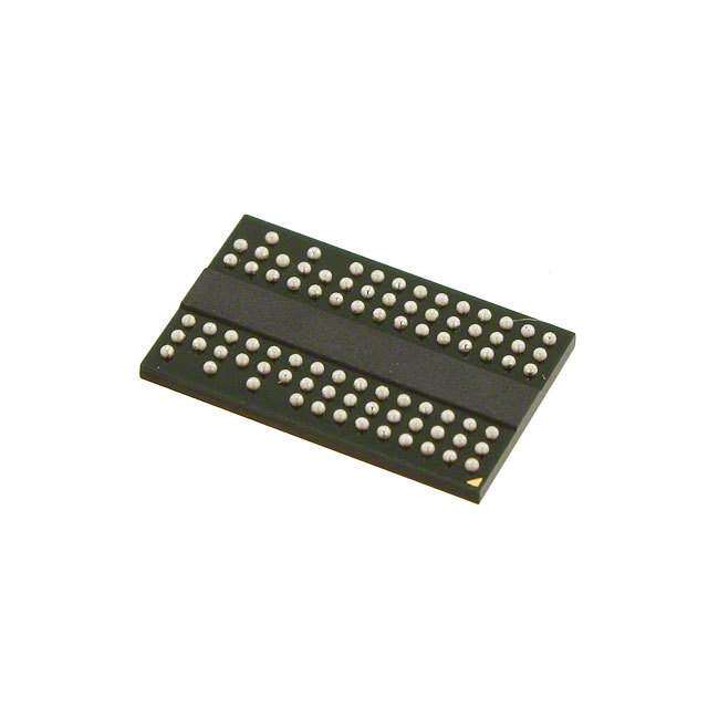
| 产品图片 |
|
| rohs | 符合RoHS无铅 / 符合限制有害物质指令(RoHS)规范要求 |
| 产品系列 | 内存,电可擦除可编程只读存储器,Microchip Technology 24LC16BT-I/SN- |
| 数据手册 | http://www.microchip.com/mymicrochip/filehandler.aspx?ddocname=en011855 |
| 产品型号 | 24LC16BT-I/SN |
| PCN设计/规格 | http://www.microchip.com/mymicrochip/NotificationDetails.aspx?pcn=JAON-29UDMC755&print=view |
| 产品培训模块 | http://www.digikey.cn/PTM/IndividualPTM.page?site=cn&lang=zhs&ptm=4315 |
| 产品目录页面 | |
| 产品种类 | 电可擦除可编程只读存储器 |
| 供应商器件封装 | 8-SOIC N |
| 其它名称 | 24LC16BT-I/SNDKR |
| 包装 | Digi-Reel® |
| 商标 | Microchip Technology |
| 存储器类型 | EEPROM |
| 存储容量 | 16K (2K x 8) |
| 安装风格 | SMD/SMT |
| 封装 | Reel |
| 封装/外壳 | 8-SOIC(0.154",3.90mm 宽) |
| 封装/箱体 | SOIC-8 |
| 工作温度 | -40°C ~ 85°C |
| 工作电流 | 3 mA |
| 工作电源电压 | 2.5 V, 5.5 V |
| 工厂包装数量 | 3300 |
| 接口 | I²C,2 线串口 |
| 接口类型 | I2C |
| 数据保留 | 200 yr |
| 最大工作温度 | + 85 C |
| 最大工作电流 | 5 mA |
| 最大时钟频率 | 0.4 MHz |
| 最小工作温度 | - 40 C |
| 标准包装 | 1 |
| 格式-存储器 | EEPROMs - 串行 |
| 电压-电源 | 2.5 V ~ 5.5 V |
| 电源电压-最大 | 5.5 V |
| 电源电压-最小 | 2.5 V |
| 组织 | 2 k x 8 |
| 访问时间 | 900 ns |
| 速度 | 400kHz |


- 商务部:美国ITC正式对集成电路等产品启动337调查
- 曝三星4nm工艺存在良率问题 高通将骁龙8 Gen1或转产台积电
- 太阳诱电将投资9.5亿元在常州建新厂生产MLCC 预计2023年完工
- 英特尔发布欧洲新工厂建设计划 深化IDM 2.0 战略
- 台积电先进制程称霸业界 有大客户加持明年业绩稳了
- 达到5530亿美元!SIA预计今年全球半导体销售额将创下新高
- 英特尔拟将自动驾驶子公司Mobileye上市 估值或超500亿美元
- 三星加码芯片和SET,合并消费电子和移动部门,撤换高东真等 CEO
- 三星电子宣布重大人事变动 还合并消费电子和移动部门
- 海关总署:前11个月进口集成电路产品价值2.52万亿元 增长14.8%


PDF Datasheet 数据手册内容提取
24AA16/24LC16B 2 16K I C™ Serial EEPROM Device Selection Table Description The Microchip Technology Inc. 24AA16/24LC16B Part Vcc Max Clock Temp (24XX16*) is a 16 Kbit Electrically Erasable PROM. Number Range Frequency Ranges The device is organized as eight blocks of 256 x 8-bit 24AA16 1.8-5.5 400kHz(1) I memory with a 2-wire serial interface. Low-voltage 24LC16B 2.5-5.5 400kHz I, E design permits operation down to 1.8V with standby and active currents of only 1µA and 1mA, Note 1: 100kHz for VCC <2.5V respectively. The 24XX16 also has a page write capability for up to 16 bytes of data. The 24XX16 is Features available in the standard 8-pin PDIP, surface mount SOIC, TSSOP and MSOP packages and is also avail- • Single supply with operation down to 1.8V able in the 5-lead SOT-23 package. (cid:127) Low-power CMOS technology - 1mA active current typical Package Types - 1µA standby current (max.) (I-temp) (cid:127) Organized as 8 blocks of 256 bytes (8 x 256 x 8) PDIP/SOIC/TSSOP/MSOP SOT-23-5 (cid:127) 2-wire serial interface bus, I 2C™ compatible A0 1 8 Vcc (cid:127) Schmitt Trigger inputs for noise suppression 2 SCL 1 5 WP A1 2 4 7 WP 2 (cid:127) Output slope control to eliminate ground bounce X 4 X Vss 2 X (cid:127) 100kHz (2.5V) and 400kHz ( ≥2.5V) compatibility A2 3 1 6 SCL X 6 1 (cid:127) Self-timed write cycle (including auto-erase) Vss 4 5 SDA SDA 3 6 4 Vcc (cid:127) Page write buffer for up to 16 bytes (cid:127) 2ms typical write cycle time for page write Note: Pins A0, A1 and A2 are not used by the (cid:127) Hardware write-protect for entire memory 24LC16B. (No internal connections). (cid:127) Can be operated as a serial ROM (cid:127) Factory programming (QTP) available Block Diagram (cid:127) ESD protection > 4,000V (cid:127) 1,000,000 erase/write cycles HV (cid:127) Data retention > 200 years WP Generator (cid:127) 8-lead PDIP, SOIC, TSSOP and MSOP packages (cid:127) 5-lead SOT-23 package (cid:127) Standard and Pb-free finishes available I/O Memory EEPROM Control Control XDEC Array (cid:127) Available temperature ranges: Logic Logic - Industrial (I): -40°C to +85°C Page Latches - Automotive (E): -40°C to +125°C I/O SCL YDEC SDA VCC Sense Amp. VSS R/W Control *24XX16 is used in this document as a generic part number for the 24AA16/24LC16B devices. 2003 Microchip Technology Inc. DS21703D-page 1
24AA16/24LC16B 1.0 ELECTRICAL CHARACTERISTICS Absolute Maximum Ratings (†) VCC.............................................................................................................................................................................6.5V All inputs and outputs w.r.t. VSS.........................................................................................................-0.3V to VCC +1.0V Storage temperature...............................................................................................................................-65°C to +150°C Ambient temperature with power applied................................................................................................-65°C to +125°C ESD protection on all pins......................................................................................................................................................≥ 4kV † NOTICE: Stresses above those listed under “Absolute Maximum Ratings” may cause permanent damage to the device. This is a stress rating only and functional operation of the device at those or any other conditions above those indicated in the operational listings of this specification is not implied. Exposure to maximum rating conditions for extended periods may affect device reliability. TABLE 1-1: DC CHARACTERISTICS VCC = +1.8V to +5.5V DC CHARACTERISTICS Industrial (I): TA = -40°C to +85°C Automotive (E): TA = -40°C to +125°C Param. Symbol Characteristic Min Typ Max Units Conditions No. D1 VIH WP, SCL and SDA pins — — — — — D2 — High-level input voltage 0.7 VCC — — V — D3 VIL Low-level input voltage — — 0.3 VCC V — D4 VHYS Hysteresis of Schmitt .05 VCC — — V (Note 1) Trigger inputs D5 VOL Low-level output voltage — — 0.40 V IOL = 3.0mA, VCC = 2.5V D6 ILI Input leakage current — — ±1 µA VIN =.1V to VCC D7 ILO Output leakage current — — ±1 µA VOUT =.1V to VCC D8 CIN, Pin capacitance — — 10 pF VCC = 5.0V (Note 1) COUT (all inputs/outputs) TA = 25°C, FCLK = 1MHz D9 ICC write Operating current — — 3 mA VCC = 5.5V, SCL = 400kHz D10 ICC read — 0.01 1 mA — D11 ICCS Standby current — 0.3 1 µA Industrial — .01 5 µA Automotive SDA = SCL = VCC WP = VSS Note 1: This parameter is periodically sampled and not 100% tested. 2: Typical measurements taken at room temperature. DS21703D-page 2 2003 Microchip Technology Inc.
24AA16/24LC16B TABLE 1-2: AC CHARACTERISTICS VCC = +1.8V to +5.5V AC CHARACTERISTICS Industrial (I): TA = -40°C to +85°C Automotive (E): TA = -40°C to +125°C Param. Symbol Characteristic Min Max Units Conditions No. 1 FCLK Clock frequency — 400 kHz 2.5V ≤ VCC ≤ 5.5V — 100 1.8V ≤ VCC < 2.5V (24AA16) 2 THIGH Clock high time 600 — ns 2.5V ≤ VCC ≤ 5.5V 4000 — 1.8V ≤ VCC < 2.5V (24AA16) 3 TLOW Clock low time 1300 — ns 2.5V ≤ VCC ≤ 5.5V 4700 — 1.8V ≤ VCC < 2.5V (24AA16) 4 TR SDA and SCL rise time — 300 ns 2.5V ≤ VCC ≤ 5.5V (Note1) (Note1) — 1000 1.8V ≤ VCC < 2.5V (24AA16) (Note1) 5 TF SDA and SCL fall time — 300 ns (Note1) 6 THD:STA Start condition hold time 600 — ns 2.5V ≤ VCC ≤ 5.5V 4000 — 1.8V ≤ VCC < 2.5V (24AA16) 7 TSU:STA Start condition setup time 600 — ns 2.5V ≤ VCC ≤ 5.5V 4700 — 1.8V ≤ VCC < 2.5V (24AA16) 8 THD:DAT Data input hold time 0 — ns (Note2) 9 TSU:DAT Data input setup time 100 — ns 2.5V ≤ VCC ≤ 5.5V 250 — 1.8V ≤ VCC < 2.5V (24AA16) 10 TSU:STO Stop condition setup time 600 — ns 2.5V ≤ VCC ≤ 5.5V 4000 — 1.8V ≤ VCC < 2.5V (24AA16) 11 TAA Output valid from clock — 900 ns 2.5V ≤ VCC ≤ 5.5V (Note2) — 3500 1.8V ≤ VCC < 2.5V (24AA16) 12 TBUF Bus free time: Time the bus 1300 — ns 2.5V ≤ VCC ≤ 5.5V must be free before a new 4700 — 1.8V ≤ VCC < 2.5V (24AA16) transmission can start 13 TOF Output fall time from VIH 20+0.1CB 250 ns 2.5V ≤ VCC ≤ 5.5V minimum to VIL maximum — 250 1.8V ≤ VCC <2.5V (24AA16) 14 TSP Input filter spike suppression — 50 ns (Notes1 and3) (SDA and SCL pins) 15 TWC Write cycle time — 5 ms — (byte or page) 16 — Endurance 1M — cycles 25°C, (Note4) Note 1: Not 100% tested. CB = total capacitance of one bus line in pF. 2: As a transmitter, the device must provide an internal minimum delay time to bridge the undefined region (minimum 300ns) of the falling edge of SCL to avoid unintended generation of Start or Stop conditions. 3: The combined TSP and VHYS specifications are due to new Schmitt Trigger inputs which provide improved noise spike suppression. This eliminates the need for a TI specification for standard operation. 4: This parameter is not tested but ensured by characterization. For endurance estimates in a specific application, please consult the Total Endurance™ Model which can be obtained from Microchip’s web site: www.microchip.com. 2003 Microchip Technology Inc. DS21703D-page 3
24AA16/24LC16B FIGURE 1-1: BUS TIMING DATA 5 4 2 3 SCL 7 8 9 10 6 SDA IN 14 11 12 SDA OUT FIGURE 1-2: BUS TIMING START/STOP D4 SCL 6 7 10 SDA Start Stop DS21703D-page 4 2003 Microchip Technology Inc.
24AA16/24LC16B 2.0 FUNCTIONAL DESCRIPTION 3.4 Data Valid (D) The 24XX16 supports a bidirectional, 2-wire bus and The state of the data line represents valid data when, data transmission protocol. A device that sends data after a Start condition, the data line is stable for the onto the bus is defined as a transmitter, while a device duration of the high period of the clock signal. receiving data is defined as a receiver. The bus has to The data on the line must be changed during the low be controlled by a master device which generates the period of the clock signal. There is one clock pulse per serial clock (SCL), controls the bus access and gener- bit of data. ates the Start and Stop conditions, while the 24XX16 Each data transfer is initiated with a Start condition and works as slave. Both master and slave can operate as terminated with a Stop condition. The number of data transmitter or receiver, but the master device deter- bytes transferred between Start and Stop conditions is mines which mode is activated. determined by the master device and is, theoretically unlimited, (although only the last sixteen will be stored 3.0 BUS CHARACTERISTICS when doing a write operation). When an overwrite does occur it will replace data in a first-in first-out (FIFO) The following bus protocol has been defined: fashion. (cid:127) Data transfer may be initiated only when the bus is not busy. 3.5 Acknowledge (cid:127) During data transfer, the data line must remain stable whenever the clock line is high. Changes in Each receiving device, when addressed, is obliged to the data line while the clock line is high will be generate an acknowledge after the reception of each interpreted as a Start or Stop condition. byte. The master device must generate an extra clock pulse which is associated with this Acknowledge bit. Accordingly, the following bus conditions have been defined (Figure3-1). Note: The 24XX16 does not generate any Acknowledge bits if an internal 3.1 Bus not Busy (A) programming cycle is in progress. The device that acknowledges, has to pull down the Both data and clock lines remain high. SDA line during the acknowledge clock pulse in such a way that the SDA line is stable low during the high 3.2 Start Data Transfer (B) period of the acknowledge related clock pulse. Of A high-to-low transition of the SDA line while the clock course, setup and hold times must be taken into (SCL) is high determines a Start condition. All account. During reads, a master must signal an end of commands must be preceded by a Start condition. data to the slave by not generating an Acknowledge bit on the last byte that has been clocked out of the slave. In this case, the slave (24XX16) will leave the data line 3.3 Stop Data Transfer (C) high to enable the master to generate the Stop A low-to-high transition of the SDA line while the clock condition. (SCL) is high determines a Stop condition. All operations must be ended with a Stop condition. FIGURE 3-1: DATA TRANSFER SEQUENCE ON THE SERIAL BUS (A) (B) (D) (D) (C) (A) SCL SDA START ADDRESS OR DATA STOP CONDITION ACKNOWLEDGE ALLOWED CONDITION VALID TO CHANGE 2003 Microchip Technology Inc. DS21703D-page 5
24AA16/24LC16B 3.6 Device Addressing FIGURE 3-2: CONTROL BYTE ALLOCATION A control byte is the first byte received following the Start condition from the master device (Figure3-2). START READ/WRITE The control byte consists of a four-bit control code. For the 24XX16, this is set as ‘1010’ binary for read and write operations. The next three bits of the control SLAVE ADDRESS R/W A byte are the block-select bits (B2, B1, B0). They are used by the master device to select which of the eight 256 word-blocks of memory are to be accessed. These bits are in effect the three Most Significant bits of the word address. It should be noted that the 1 0 1 0 B2 B1 B0 protocol limits the size of the memory to eight blocks of 256 words, therefore the protocol can support only one 24XX16 per system. The last bit of the control byte defines the operation to be performed. When set to ‘1’, a read operation is selected. When set to ‘0’, a write operation is selected. Following the Start condition, the 24XX16 monitors the SDA bus checking the device type identifier being transmitted and, upon receiving a ‘1010’ code, the slave device outputs an Acknowledge signal on the SDA line. Depending on the state of the R/W bit, the 24XX16 will select a read or write operation. Control Operation Block Select R/W Code Read 1010 Block Address 1 Write 1010 Block Address 0 DS21703D-page 6 2003 Microchip Technology Inc.
24AA16/24LC16B 4.0 WRITE OPERATION 4.2 Page Write The write control byte, word address and the first data 4.1 Byte Write byte are transmitted to the 24XX16 in the same way as in a byte write. However, instead of generating a Stop Following the Start condition from the master, the condition, the master transmits up to 16 data bytes to device code (4 bits), the block address (3 bits) and the the 24XX16, which are temporarily stored in the on- R/W bit, which is a logic-low, is placed onto the bus by chip page buffer and will be written into memory once the master transmitter. This indicates to the addressed the master has transmitted a Stop condition. Upon slave receiver that a byte with a word address will receipt of each word, the four lower-order address follow once it has generated an Acknowledge bit during pointer bits are internally incremented by ‘1’. The the ninth clock cycle. Therefore, the next byte transmit- higher-order 7 bits of the word address remain ted by the master is the word address and will be constant. If the master should transmit more than 16 written into the address pointer of the 24XX16. After bytes prior to generating the Stop condition, the receiving another Acknowledge signal from the address counter will roll over and the previously 24XX16, the master device will transmit the data word received data will be overwritten. As with the byte write to be written into the addressed memory location. The operation, once the Stop condition is received an inter- 24XX16 acknowledges again and the master nal write cycle will begin (Figure4-2). generates a Stop condition. This initiates the internal write cycle and, during this time, the 24XX16 will not Note: Page write operations are limited to writing generate Acknowledge signals (Figure4-1). bytes within a single physical page, regardless of the number of bytes actually being written. Physical page boundaries start at addresses that are integer multiples of the page buffer size (or ‘page-size’) and end at addresses that are integer multiples of [page size - 1]. If a Page Write command attempts to write across a physical page boundary, the result is that the data wraps around to the beginning of the current page (overwriting data previously stored there), instead of being written to the next page, as might be expected. It is therefore necessary for the application software to prevent page write operations that would attempt to cross a page boundary. FIGURE 4-1: BYTE WRITE S S BUS ACTIVITY T CONTROL WORD T MASTER A BYTE ADDRESS DATA O R P T SDA LINE S P A A A BUS ACTIVITY C C C K K K FIGURE 4-2: PAGE WRITE S S BUS ACTIVITY T CONTROL WORD T MASTER AR BYTE ADDRESS (n) DATA (n) DATA (n + 1) DATA (n + 15) OP T SDA LINE S P A A A A A BUS ACTIVITY C C C C C K K K K K 2003 Microchip Technology Inc. DS21703D-page 7
24AA16/24LC16B 5.0 ACKNOWLEDGE POLLING 6.0 WRITE-PROTECTION Since the device will not acknowledge during a write The 24XX16 can be used as a serial ROM when the cycle, this can be used to determine when the cycle is WP pin is connected to VCC. Programming will be complete (this feature can be used to maximize bus inhibited and the entire memory will be write-protected. throughput). Once the Stop condition for a write command has been issued from the master, the device initiates the internally-timed write cycle and ACK polling can then be initiated immediately. This involves the master sending a Start condition followed by the control byte for a Write command (R/W = 0). If the device is still busy with the write cycle, no ACK will be returned. If the cycle is complete, the device will return the ACK and the master can then proceed with the next Read or Write command. See Figure5-1 for a flow diagram of this operation. FIGURE 5-1: ACKNOWLEDGE POLLING FLOW Send Write Command Send Stop Condition to Initiate Write Cycle Send Start Send Control Byte with R/W = 0 Did Device No Acknowledge (ACK = 0)? Yes Next Operation DS21703D-page 8 2003 Microchip Technology Inc.
24AA16/24LC16B 7.0 READ OPERATION 7.3 Sequential Read Read operations are initiated in the same way as write Sequential reads are initiated in the same way as a operations, with the exception that the R/W bit of the random read, except that once the 24XX16 transmits slave address is set to ‘1’. There are three basic types the first data byte, the master issues an acknowledge of read operations: current address read, random read as opposed to a Stop condition in a random read. This and sequential read. directs the 24XX16 to transmit the next sequentially- addressed 8-bit word (Figure7-3). 7.1 Current Address Read To provide sequential reads, the 24XX16 contains an internal address pointer that is incremented by one The 24XX16 contains an address counter that main- upon completion of each operation. This address tains the address of the last word accessed, internally pointer allows the entire memory contents to be serially incremented by ‘1’. Therefore, if the previous access read during one operation. (either a read or write operation) was to address n, the next current address read operation would access data 7.4 Noise Protection from address n + 1. Upon receipt of the slave address with R/W bit set to ‘1’, the 24XX16 issues an acknowl- The 24XX16 employs a VCC threshold detector circuit edge and transmits the 8-bit data word. The master will which disables the internal erase/write logic if the VCC not acknowledge the transfer but does generate a Stop is below 1.5V at nominal conditions. condition and the 24XX16 discontinues transmission The SCL and SDA inputs have Schmitt Trigger and (Figure7-1). filter circuits which suppress noise spikes to assure proper device operation, even on a noisy bus. 7.2 Random Read Random read operations allow the master to access any memory location in a random manner. To perform this type of read operation, the word address must first be set. This is accomplished by sending the word address to the 24XX16 as part of a write operation. Once the word address is sent, the master generates a Start condition following the acknowledge. This terminates the write operation, but not before the inter- nal address pointer is set. The master then issues the control byte again, but with the R/W bit set to a ‘1’. The 24XX16 will then issue an acknowledge and transmit the 8-bit data word. The master will not acknowledge the transfer but does generate a Stop condition and the 24XX16 will discontinue transmission (Figure7-2). FIGURE 7-1: CURRENT ADDRESS READ S BUS ACTIVITY T CONTROL S MASTER A BYTE DATA (n) T R O T P SDA LINE S P A N BUS ACTIVITY C O K A C K 2003 Microchip Technology Inc. DS21703D-page 9
24AA16/24LC16B FIGURE 7-2: RANDOM READ S S BUS ACTIVITY T CONTROL WORD T CONTROL S A A T MASTER R BYTE ADDRESS (n) R BYTE DATA (n) O T T P S S P SDA LINE A A A N C C C O K K K BUS ACTIVITY A C K FIGURE 7-3: SEQUENTIAL READ S BUS ACTIVITY CONTROL T MASTER BYTE DATA (n) DATA (n + 1) DATA (n + 2) DATA (n + X) O P SDA LINE P A A A A N BUS ACTIVITY C C C C O K K K K A C K DS21703D-page 10 2003 Microchip Technology Inc.
24AA16/24LC16B 8.0 PIN DESCRIPTIONS The descriptions of the pins are listed in Table8-1. TABLE 8-1: PIN FUNCTION TABLE Name PDIP SOIC TSSOP MSOP SOT-23 Description A0 1 1 1 1 — Not Connected A1 2 2 2 2 — Not Connected A2 3 3 3 3 — Not Connected VSS 4 4 4 4 2 Ground SDA 5 5 5 5 3 Serial Address/Data I/O SCL 6 6 6 6 1 Serial Clock WP 7 7 7 7 5 Write-Protect Input VCC 8 8 8 8 4 +1.8V to 5.5V Power Supply 8.1 Serial Address/Data Input/Output 8.3 Write-Protect (WP) (SDA) The WP pin must be connected to either VSS or VCC. SDA is a bidirectional pin used to transfer addresses If tied to VSS, normal memory operation is enabled and data into and out of the device. Since it is an open- (read/write the entire memory 00-07FFH). drain terminal, the SDA bus requires a pull-up resistor to VCC (typical 10kΩ for 100kHz, 2kΩ for 400kHz). If tied to VCC, write operations are inhibited. The entire memory will be write-protected. Read operations are For normal data transfer, SDA is allowed to change not affected. only during SCL low. Changes during SCL high are This feature allows the user to use the 24XX16 as a reserved for indicating Start and Stop conditions. serial ROM when WP is enabled (tied to VCC). 8.2 Serial Clock (SCL) 8.4 A0, A1, A2 The SCL input is used to synchronize the data transfer The A0, A1 and A2 pins are not used by the 24XX16. to and from the device. They may be left floating or tied to either VSS or VCC. 2003 Microchip Technology Inc. DS21703D-page 11
24AA16/24LC16B 9.0 PACKAGING INFORMATION 9.1 Package Marking Information 8-Lead PDIP (300 mil) Example: XXXXXXXX 24LC16B T/XXXNNN I/P13F YYWW 0327 8-Lead SOIC (150 mil) Example: XXXXXXXX 24LC16B T/XXYYWW I/SNYYWW NNN 13F 8-Lead TSSOP Example: TSSOP/MSOP XXXX 4L16 Device Marking Codes TYWW I327 STD Pb-free NNN 13F 24AA16 4A16 G4A6 24LC16B 4L16 G4L6 8-Lead MSOP Example: XXXXXT 4L16BI YWWNNN 32713F SOT-23 5-Lead SOT-23 Example: Marking Codes Device STD Pb-free 24AA16 B5 B5 XXNN B53F 24LC16B-I M5 M5 24LC16B-E N5 N5 Note: Pb-free part number using “G” suffix is marked on carton Legend: XX...X Customer specific information* T Temperature grade (I, E) YY Year code (last 2 digits of calendar year) WW Week code (week of January 1 is week ‘01’) NNN Alphanumeric traceability code Note: In the event the full Microchip part number cannot be marked on one line, it will be carried over to the next line thus limiting the number of available characters for customer specific information. *Standard QTP marking consists of Microchip part number, year code, week code, and traceability code. DS21703D-page 12 2003 Microchip Technology Inc.
24AA16/24LC16B 8-Lead Plastic Dual In-line (P) – 300 mil (PDIP) E1 D 2 n 1 α E A A2 L c A1 β B1 p eB B Units INCHES* MILLIMETERS Dimension Limits MIN NOM MAX MIN NOM MAX Number of Pins n 8 8 Pitch p .100 2.54 Top to Seating Plane A .140 .155 .170 3.56 3.94 4.32 Molded Package Thickness A2 .115 .130 .145 2.92 3.30 3.68 Base to Seating Plane A1 .015 0.38 Shoulder to Shoulder Width E .300 .313 .325 7.62 7.94 8.26 Molded Package Width E1 .240 .250 .260 6.10 6.35 6.60 Overall Length D .360 .373 .385 9.14 9.46 9.78 Tip to Seating Plane L .125 .130 .135 3.18 3.30 3.43 Lead Thickness c .008 .012 .015 0.20 0.29 0.38 Upper Lead Width B1 .045 .058 .070 1.14 1.46 1.78 Lower Lead Width B .014 .018 .022 0.36 0.46 0.56 Overall Row Spacing § eB .310 .370 .430 7.87 9.40 10.92 Mold Draft Angle Top α 5 10 15 5 10 15 Mold Draft Angle Bottom β 5 10 15 5 10 15 * Controlling Parameter § Significant Characteristic Notes: Dimensions D and E1 do not include mold flash or protrusions. Mold flash or protrusions shall not exceed .010” (0.254mm) per side. JEDEC Equivalent: MS-001 Drawing No. C04-018 2003 Microchip Technology Inc. DS21703D-page 13
24AA16/24LC16B 8-Lead Plastic Small Outline (SN) –Narrow, 150 mil (SOIC) E E1 p D 2 B n 1 h α 45° c A A2 φ β L A1 Units INCHES* MILLIMETERS Dimension Limits MIN NOM MAX MIN NOM MAX Number of Pins n 8 8 Pitch p .050 1.27 Overall Height A .053 .061 .069 1.35 1.55 1.75 Molded Package Thickness A2 .052 .056 .061 1.32 1.42 1.55 Standoff § A1 .004 .007 .010 0.10 0.18 0.25 Overall Width E .228 .237 .244 5.79 6.02 6.20 Molded Package Width E1 .146 .154 .157 3.71 3.91 3.99 Overall Length D .189 .193 .197 4.80 4.90 5.00 Chamfer Distance h .010 .015 .020 0.25 0.38 0.51 Foot Length L .019 .025 .030 0.48 0.62 0.76 Foot Angle φ 0 4 8 0 4 8 Lead Thickness c .008 .009 .010 0.20 0.23 0.25 Lead Width B .013 .017 .020 0.33 0.42 0.51 Mold Draft Angle Top α 0 12 15 0 12 15 Mold Draft Angle Bottom β 0 12 15 0 12 15 * Controlling Parameter § Significant Characteristic Notes: Dimensions D and E1 do not include mold flash or protrusions. Mold flash or protrusions shall not exceed .010” (0.254mm) per side. JEDEC Equivalent: MS-012 Drawing No. C04-057 DS21703D-page 14 2003 Microchip Technology Inc.
24AA16/24LC16B 8-Lead Plastic Thin Shrink Small Outline (ST) – 4.4 mm (TSSOP) E E1 p D 2 1 n B α A c φ A1 A2 β L Units INCHES MILLIMETERS* Dimension Limits MIN NOM MAX MIN NOM MAX Number of Pins n 8 8 Pitch p .026 0.65 Overall Height A .043 1.10 Molded Package Thickness A2 .033 .035 .037 0.85 0.90 0.95 Standoff § A1 .002 .004 .006 0.05 0.10 0.15 Overall Width E .246 .251 .256 6.25 6.38 6.50 Molded Package Width E1 .169 .173 .177 4.30 4.40 4.50 Molded Package Length D .114 .118 .122 2.90 3.00 3.10 Foot Length L .020 .024 .028 0.50 0.60 0.70 Foot Angle φ 0 4 8 0 4 8 Lead Thickness c .004 .006 .008 0.09 0.15 0.20 Lead Width B .007 .010 .012 0.19 0.25 0.30 Mold Draft Angle Top α 0 5 10 0 5 10 Mold Draft Angle Bottom β 0 5 10 0 5 10 * Controlling Parameter § Significant Characteristic Notes: Dimensions D and E1 do not include mold flash or protrusions. Mold flash or protrusions shall not exceed .005” (0.127mm) per side. JEDEC Equivalent: MO-153 Drawing No. C04-086 8-Lead Plastic Micro Small Outline Package (MS) (MSOP) 2003 Microchip Technology Inc. DS21703D-page 15
24AA16/24LC16B E E1 p D 2 B n 1 α A A2 c φ A1 (F) L β Units INCHES MILLIMETERS* Dimension Limits MIN NOM MAX MIN NOM MAX Number of Pins n 8 8 Pitch p .026 BSC 0.65 BSC Overall Height A - - .043 - - 1.10 Molded Package Thickness A2 .030 .033 .037 0.75 0.85 0.95 Standoff A1 .000 - .006 0.00 - 0.15 Overall Width E .193 TYP. 4.90 BSC Molded Package Width E1 .118 BSC 3.00 BSC Overall Length D .118 BSC 3.00 BSC Foot Length L .016 .024 .031 0.40 0.60 0.80 Footprint (Reference) F .037 REF 0.95 REF Foot Angle φ 0° - 8° 0° - 8° Lead Thickness c .003 .006 .009 0.08 - 0.23 Lead Width B .009 .012 .016 0.22 - 0.40 Mold Draft Angle Top α 5° - 15° 5° - 15° Mold Draft Angle Bottom β 5° - 15° 5° - 15° *Controlling Parameter Notes: Dimensions D and E1 do not include mold flash or protrusions. Mold flash or protrusions shall not exceed .010" (0.254mm) per side. JEDEC Equivalent: MO-187 Drawing No. C04-111 DS21703D-page 16 2003 Microchip Technology Inc.
24AA16/24LC16B APPENDIX A: REVISION HISTORY Revision D Corrections to Section 1.0, Electrical Characteristics. 2003 Microchip Technology Inc. DS21703D-page 17
24AA16/24LC16B NOTES: DS21703D-page 18 2003 Microchip Technology Inc.
24AA16/24LC16B ON-LINE SUPPORT SYSTEMS INFORMATION AND UPGRADE HOT LINE Microchip provides on-line support on the Microchip World Wide Web site. The Systems Information and Upgrade Line provides The web site is used by Microchip as a means to make system users a listing of the latest versions of all of files and information easily available to customers. To Microchip's development systems software products. view the site, the user must have access to the Internet Plus, this line provides information on how customers and a web browser, such as Netscape® or Microsoft® can receive the most current upgrade kits. The Hot Line Internet Explorer. Files are also available for FTP Numbers are: download from our FTP site. 1-800-755-2345 for U.S. and most of Canada, and 1-480-792-7302 for the rest of the world. Connecting to the Microchip Internet Web Site 042003 The Microchip web site is available at the following URL: www.microchip.com The file transfer site is available by using an FTP service to connect to: ftp://ftp.microchip.com The web site and file transfer site provide a variety of services. Users may download files for the latest Development Tools, Data Sheets, Application Notes, User's Guides, Articles and Sample Programs. A vari- ety of Microchip specific business information is also available, including listings of Microchip sales offices, distributors and factory representatives. Other data available for consideration is: (cid:127) Latest Microchip Press Releases (cid:127) Technical Support Section with Frequently Asked Questions (cid:127) Design Tips (cid:127) Device Errata (cid:127) Job Postings (cid:127) Microchip Consultant Program Member Listing (cid:127) Links to other useful web sites related to Microchip Products (cid:127) Conferences for products, Development Systems, technical information and more (cid:127) Listing of seminars and events 2003 Microchip Technology Inc. DS21703D-page 19
24AA16/24LC16B READER RESPONSE It is our intention to provide you with the best documentation possible to ensure successful use of your Microchip prod- uct. If you wish to provide your comments on organization, clarity, subject matter, and ways in which our documentation can better serve you, please FAX your comments to the Technical Publications Manager at (480) 792-4150. Please list the following information, and use this outline to provide us with your comments about this document. To: Technical Publications Manager Total Pages Sent ________ RE: Reader Response From: Name Company Address City / State / ZIP / Country Telephone: (_______) _________ - _________ FAX: (______) _________ - _________ Application (optional): Would you like a reply? Y N Device: 24AA16/24LC16B Literature Number: DS21703D Questions: 1. What are the best features of this document? 2. How does this document meet your hardware and software development needs? 3. Do you find the organization of this document easy to follow? If not, why? 4. What additions to the document do you think would enhance the structure and subject? 5. What deletions from the document could be made without affecting the overall usefulness? 6. Is there any incorrect or misleading information (what and where)? 7. How would you improve this document? DS21703D-page 20 2003 Microchip Technology Inc.
24AA16/24LC16B PRODUCT IDENTIFICATION SYSTEM To order or obtain information, e.g., on pricing or delivery, refer to the factory or the listed sales office. PART NO. X /XX X Examples: Device Temperature Package Lead Finish a) 24AA16-I/P: Industrial Temperature,1.8V, Range PDIP package b) 24AA16-I/SN: Industrial Temperature,1.8V, 24AA16: = 1.8V, 16 Kbit I2C Serial EEPROM SOIC package 24AA16T: = 1.8V, 16 Kbit I2C Serial EEPROM c) 24AA16T-I/OT: Industrial Temperature, (Tape and Reel) 1.8V, SOT-23 package, Tape and Reel 24LC16B: = 2.5V, 16 Kbit I2C Serial EEPROM 24LC16BT: = 2.5V, 16 Kbit I2C Serial EEPROM (Tape and Reel) d) 24LC16B-I/P: Industrial Temperature, 2.5V, PDIP package e) 24LC16B-E/SN: Automotive Temp.,2.5V Tempera- I =-40°C to +85°C SOIC package ture E =-40°C to +125°C f) 24LC16BT-I/OT: Industrial Temperature, Range: 2.5V, SOT-23 package, Tape and Reel g) 24LC16B-I/PG: Industrial Temperature, Package: P = Plastic DIP (300 mil body), 8-lead 2.5V, PDIP package, Pb-free SN = Plastic SOIC (150 mil body), 8-lead h) 24LC16BT-I/SNG: Industrial Temperature, ST = Plastic TSSOP (4.4 mm), 8-lead 2.5V, SOIC package, Tape and Reel, MS = Plastic Micro Small Outline (MSOP), 8-lead Pb-free OT = SOT-23, 5-lead (Tape and Reel only) Lead Finish Blank = Standard 63% / 37% SnPb G = Pb-free (Matte Tin - Pure Sn) Sales and Support Data Sheets Products supported by a preliminary Data Sheet may have an errata sheet describing minor operational differences and recommended workarounds. To determine if an errata sheet exists for a particular device, please contact one of the following: 1. Your local Microchip sales office 2. The Microchip Corporate Literature Center U.S. FAX: (480) 792-7277 3. The Microchip Worldwide Site (www.microchip.com) Please specify which device, revision of silicon and Data Sheet (include Literature #) you are using. New Customer Notification System Register on our web site (www.microchip.com/cn) to receive the most current information on our products. 2003 Microchip Technology Inc. DS21703D-page 21
24AA16/24LC16B NOTES: DS21703D-page 22 2003 Microchip Technology Inc.
Note the following details of the code protection feature on Microchip devices: (cid:127) Microchip products meet the specification contained in their particular Microchip Data Sheet. (cid:127) Microchip believes that its family of products is one of the most secure families of its kind on the market today, when used in the intended manner and under normal conditions. (cid:127) There are dishonest and possibly illegal methods used to breach the code protection feature. All of these methods, to our knowledge, require using the Microchip products in a manner outside the operating specifications contained in Microchip's Data Sheets. Most likely, the person doing so is engaged in theft of intellectual property. (cid:127) Microchip is willing to work with the customer who is concerned about the integrity of their code. (cid:127) Neither Microchip nor any other semiconductor manufacturer can guarantee the security of their code. Code protection does not mean that we are guaranteeing the product as “unbreakable.” Code protection is constantly evolving. We at Microchip are committed to continuously improving the code protection features of our products. Attempts to break microchip’s code protection feature may be a violation of the Digital Millennium Copyright Act. If such acts allow unauthorized access to your software or other copyrighted work, you may have a right to sue for relief under that Act. Information contained in this publication regarding device Trademarks applications and the like is intended through suggestion only The Microchip name and logo, the Microchip logo, Accuron, and may be superseded by updates. It is your responsibility to dsPIC, KEELOQ, MPLAB, PIC, PICmicro, PICSTART, ensure that your application meets with your specifications. PRO MATE and PowerSmart are registered trademarks of No representation or warranty is given and no liability is Microchip Technology Incorporated in the U.S.A. and other assumed by Microchip Technology Incorporated with respect countries. to the accuracy or use of such information, or infringement of patents or other intellectual property rights arising from such AmpLab, FilterLab, microID, MXDEV, MXLAB, PICMASTER, use or otherwise. Use of Microchip’s products as critical com- SEEVAL and The Embedded Control Solutions Company are ponents in life support systems is not authorized except with registered trademarks of Microchip Technology Incorporated express written approval by Microchip. No licenses are con- in the U.S.A. veyed, implicitly or otherwise, under any intellectual property Application Maestro, dsPICDEM, dsPICDEM.net, ECAN, rights. ECONOMONITOR, FanSense, FlexROM, fuzzyLAB, In-Circuit Serial Programming, ICSP, ICEPIC, microPort, Migratable Memory, MPASM, MPLIB, MPLINK, MPSIM, PICkit, PICDEM, PICDEM.net, PowerCal, PowerInfo, PowerMate, PowerTool, rfLAB, rfPIC, Select Mode, SmartSensor, SmartShunt, SmartTel and Total Endurance are trademarks of Microchip Technology Incorporated in the U.S.A. and other countries. Serialized Quick Turn Programming (SQTP) is a service mark of Microchip Technology Incorporated in the U.S.A. All other trademarks mentioned herein are property of their respective companies. © 2003, Microchip Technology Incorporated, Printed in the U.S.A., All Rights Reserved. Printed on recycled paper. Microchip received QS-9000 quality system certification for its worldwide headquarters, design and wafer fabrication facilities in Chandler and Tempe, Arizona in July 1999 and Mountain View, California in March 2002. The Company’s quality system processes and procedures are QS-9000 compliant for its PICmicro® 8-bit MCUs, KEELOQ® code hopping devices, Serial EEPROMs, microperipherals, non-volatile memory and analog products. In addition, Microchip’s quality system for the design and manufacture of development systems is ISO 9001 certified. 2003 Microchip Technology Inc. DS21703D-page 23
WORLDWIDE SALES AND SERVICE AMERICAS ASIA/PACIFIC Korea Corporate Office Australia 168-1, Youngbo Bldg. 3 Floor Samsung-Dong, Kangnam-Ku 2355 West Chandler Blvd. Suite 22, 41 Rawson Street Seoul, Korea 135-882 Chandler, AZ 85224-6199 Epping 2121, NSW Tel: 82-2-554-7200 Fax: 82-2-558-5932 or Tel: 480-792-7200 Australia 82-2-558-5934 Fax: 480-792-7277 Tel: 61-2-9868-6733 Singapore Technical Support: 480-792-7627 Fax: 61-2-9868-6755 Web Address: http://www.microchip.com China - Beijing 200 Middle Road #07-02 Prime Centre Atlanta Unit 915 Singapore, 188980 3780 Mansell Road, Suite 130 Bei Hai Wan Tai Bldg. Tel: 65-6334-8870 Fax: 65-6334-8850 Alpharetta, GA 30022 No. 6 Chaoyangmen Beidajie Taiwan Tel: 770-640-0034 Beijing, 100027, No. China Fax: 770-640-0307 Tel: 86-10-85282100 Kaohsiung Branch Fax: 86-10-85282104 30F - 1 No. 8 Boston China - Chengdu Min Chuan 2nd Road 2 Lan Drive, Suite 120 Kaohsiung 806, Taiwan Rm. 2401-2402, 24th Floor, Westford, MA 01886 Tel: 886-7-536-4818 Tel: 978-692-3848 Ming Xing Financial Tower Fax: 886-7-536-4803 No. 88 TIDU Street Fax: 978-692-3821 Taiwan Chengdu 610016, China Chicago Tel: 86-28-86766200 Taiwan Branch 333 Pierce Road, Suite 180 Fax: 86-28-86766599 11F-3, No. 207 Itasca, IL 60143 China - Fuzhou Tung Hua North Road Tel: 630-285-0071 Taipei, 105, Taiwan Fax: 630-285-0075 Unit 28F, World Trade Plaza Tel: 886-2-2717-7175 Fax: 886-2-2545-0139 No. 71 Wusi Road Dallas Fuzhou 350001, China EUROPE 4570 Westgrove Drive, Suite 160 Tel: 86-591-7503506 Austria Addison, TX 75001 Fax: 86-591-7503521 Tel: 972-818-7423 China - Hong Kong SAR Durisolstrasse 2 Fax: 972-818-2924 Unit 901-6, Tower 2, Metroplaza AA-u4s6tr0ia0 Wels Detroit 223 Hing Fong Road Tel: 43-7242-2244-399 Tri-Atria Office Building Kwai Fong, N.T., Hong Kong Fax: 43-7242-2244-393 32255 Northwestern Highway, Suite 190 Tel: 852-2401-1200 Denmark Farmington Hills, MI 48334 Fax: 852-2401-3431 Regus Business Centre Tel: 248-538-2250 China - Shanghai Lautrup hoj 1-3 Fax: 248-538-2260 Room 701, Bldg. B Ballerup DK-2750 Denmark Kokomo Far East International Plaza Tel: 45-4420-9895 Fax: 45-4420-9910 2767 S. Albright Road No. 317 Xian Xia Road France Kokomo, IN 46902 Shanghai, 200051 Parc d’Activite du Moulin de Massy Tel: 765-864-8360 Tel: 86-21-6275-5700 43 Rue du Saule Trapu Fax: 765-864-8387 Fax: 86-21-6275-5060 Batiment A - ler Etage Los Angeles China - Shenzhen 91300 Massy, France Rm. 1812, 18/F, Building A, United Plaza Tel: 33-1-69-53-63-20 18201 Von Karman, Suite 1090 No. 5022 Binhe Road, Futian District Fax: 33-1-69-30-90-79 Irvine, CA 92612 Shenzhen 518033, China Germany Tel: 949-263-1888 Tel: 86-755-82901380 Steinheilstrasse 10 Fax: 949-263-1338 Fax: 86-755-8295-1393 D-85737 Ismaning, Germany Phoenix China - Shunde Tel: 49-89-627-144-0 2355 West Chandler Blvd. Room 401, Hongjian Building Fax: 49-89-627-144-44 Chandler, AZ 85224-6199 No. 2 Fengxiangnan Road, Ronggui Town Italy Tel: 480-792-7966 Shunde City, Guangdong 528303, China Via Quasimodo, 12 Fax: 480-792-4338 Tel: 86-765-8395507 Fax: 86-765-8395571 20025 Legnano (MI) San Jose China - Qingdao Milan, Italy 2107 North First Street, Suite 590 Rm. B505A, Fullhope Plaza, Tel: 39-0331-742611 San Jose, CA 95131 No. 12 Hong Kong Central Rd. Fax: 39-0331-466781 Tel: 408-436-7950 Qingdao 266071, China Netherlands Fax: 408-436-7955 Tel: 86-532-5027355 Fax: 86-532-5027205 P. A. De Biesbosch 14 Toronto India NL-5152 SC Drunen, Netherlands 6285 Northam Drive, Suite 108 Divyasree Chambers Tel: 31-416-690399 Mississauga, Ontario L4V 1X5, Canada 1 Floor, Wing A (A3/A4) Fax: 31-416-690340 Tel: 905-673-0699 No. 11, O’Shaugnessey Road United Kingdom Fax: 905-673-6509 Bangalore, 560 025, India 505 Eskdale Road Tel: 91-80-2290061 Fax: 91-80-2290062 Winnersh Triangle Japan Wokingham Benex S-1 6F Berkshire, England RG41 5TU 3-18-20, Shinyokohama Tel: 44-118-921-5869 Kohoku-Ku, Yokohama-shi Fax: 44-118-921-5820 Kanagawa, 222-0033, Japan Tel: 81-45-471- 6166 Fax: 81-45-471-6122 07/28/03 DS21703D-page 24 2003 Microchip Technology Inc.
Mouser Electronics Authorized Distributor Click to View Pricing, Inventory, Delivery & Lifecycle Information: M icrochip: 24LC16B-E/P 24AA16-I/SN 24AA16-I/MS 24AA16-I/MC 24AA16T-I/ST 24AA16T-I/OT 24AA16T-I/SN 24AA16T- I/MS 24AA16T-I/MC 24AA16-I/P 24LC16BT-E/SN 24LC16BT-E/OT 24LC16BT-E/ST 24LC16BT-E/MS 24LC16BT/ST 24LC16BT/SN 24LC16B-E/ST 24LC16B-E/SN 24LC16B-E/MS 24LC16BT-I/OTG 24LC16B/ST 24LC16B-I/P 24LC16B-I/MS 24LC16B-I/ST 24LC16B-I/SN 24LC16B/SN 24LC16B-I/STG 24LC16B-I/SNG 24AA16T/ST 24AA16/P 24AA16-I/ST 24LC16BT-I/OT 24LC16BT-I/MS 24LC16BT-I/SN 24LC16B/P