ICGOO在线商城 > 24AA16HT-I/OT

 Datasheet下载
- 型号: 24AA16HT-I/OT
- 制造商: Microchip
- 库位|库存: xxxx|xxxx
- 要求:
| 数量阶梯 | 香港交货 | 国内含税 |
| +xxxx | $xxxx | ¥xxxx |
查看当月历史价格
查看今年历史价格
24AA16HT-I/OT产品简介:
ICGOO电子元器件商城为您提供24AA16HT-I/OT由Microchip设计生产,在icgoo商城现货销售,并且可以通过原厂、代理商等渠道进行代购。 提供24AA16HT-I/OT价格参考以及Microchip24AA16HT-I/OT封装/规格参数等产品信息。 你可以下载24AA16HT-I/OT参考资料、Datasheet数据手册功能说明书, 资料中有24AA16HT-I/OT详细功能的应用电路图电压和使用方法及教程。
| 参数 | 数值 |
| 产品目录 | 集成电路 (IC)半导体 |
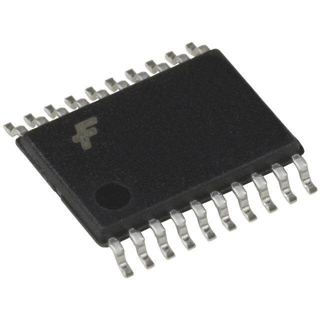
| 描述 | IC EEPROM 16KBIT 400KHZ SOT23-5电可擦除可编程只读存储器 16K 2KX8 1.8V SERIAL EE IND 1/2 ARRAY WP |
| 产品分类 | |
| 品牌 | Microchip Technology |
| 产品手册 | |
| 产品图片 |
|
| rohs | 符合RoHS无铅 / 符合限制有害物质指令(RoHS)规范要求 |
| 产品系列 | 内存,电可擦除可编程只读存储器,Microchip Technology 24AA16HT-I/OT- |
| 数据手册 | http://www.microchip.com/mymicrochip/filehandler.aspx?ddocname=en538685 |
| 产品型号 | 24AA16HT-I/OT |
| 产品目录页面 | |
| 产品种类 | 电可擦除可编程只读存储器 |
| 供应商器件封装 | SOT-23-5 |
| 其它名称 | 24AA16HT-I/OTDKR |
| 包装 | Digi-Reel® |
| 商标 | Microchip Technology |
| 存储器类型 | EEPROM |
| 存储容量 | 16K (2K x 8) |
| 安装风格 | SMD/SMT |
| 封装 | Reel |
| 封装/外壳 | SC-74A,SOT-753 |
| 封装/箱体 | SOT-23-5 |
| 工作温度 | -40°C ~ 85°C |
| 工作电流 | 3 mA |
| 工作电源电压 | 1.8 V to 5.5 V |
| 工厂包装数量 | 3000 |
| 接口 | I²C,2 线串口 |
| 接口类型 | I2C |
| 数据保留 | 200 yr |
| 最大工作温度 | + 85 C |
| 最大工作电流 | 3 mA |
| 最大时钟频率 | 0.1 MHz |
| 最小工作温度 | - 40 C |
| 标准包装 | 1 |
| 格式-存储器 | EEPROMs - 串行 |
| 电压-电源 | 1.7 V ~ 5.5 V |
| 电源电压-最大 | 5.5 V |
| 电源电压-最小 | 1.8 V |
| 组织 | 2 k x 8 |
| 访问时间 | 3500 ns |
| 速度 | 100kHz,400kHz |


- 商务部:美国ITC正式对集成电路等产品启动337调查
- 曝三星4nm工艺存在良率问题 高通将骁龙8 Gen1或转产台积电
- 太阳诱电将投资9.5亿元在常州建新厂生产MLCC 预计2023年完工
- 英特尔发布欧洲新工厂建设计划 深化IDM 2.0 战略
- 台积电先进制程称霸业界 有大客户加持明年业绩稳了
- 达到5530亿美元!SIA预计今年全球半导体销售额将创下新高
- 英特尔拟将自动驾驶子公司Mobileye上市 估值或超500亿美元
- 三星加码芯片和SET,合并消费电子和移动部门,撤换高东真等 CEO
- 三星电子宣布重大人事变动 还合并消费电子和移动部门
- 海关总署:前11个月进口集成电路产品价值2.52万亿元 增长14.8%

PDF Datasheet 数据手册内容提取
24AA16H/24LC16BH 2 16K I C™ Serial EEPROM with Half-Array Write-Protect Device Selection Table Description: Part VCC Max. Clock Temp. The Microchip Technology Inc. 24AA16H/24LC16BH Number Range Frequency Ranges (24XX16H*) is an 16 Kbit Electrically Erasable PROM. 24AA16H 1.7-5.5 400 kHz(1) I The device is organized as eight blocks of 256 x 8-bit memory with a 2-wire serial interface. Low-voltage 24LC16BH 2.5-5.5 400 kHz I, E design permits operation down to 1.7V, with standby Note 1: 100 kHz for VCC <2.5V and active currents of only 1 μA and 1 mA, respectively. The 24XX16H also has a page write Features: capability for up to 16 bytes of data. The 24XX16H is available in the standard 8-pin PDIP, surface mount • Single Supply with Operation Down to 1.7V for SOIC, TSSOP, 2x3 TDFN and MSOP packages, and 24AA16H Devices, 2.5V for 24LC16BH Devices is also available in the 5-lead SOT-23 package. All • Low-Power CMOS Technology: packages are Pb-free and RoHS compliant. - Read current 1 mA, max. Block Diagram - Standby current 1 μA, max. • 2-Wire Serial Interface, I2C™ Compatible HV WP Generator • Schmitt Trigger Inputs for Noise Suppression • Output Slope Control to eliminate Ground Bounce • 100 kHz and 400 kHz Clock Compatibility I/O Memory EEPROM • Page Write Time 3 ms, typical Control Control XDEC Array Logic Logic • Self-Timed Erase/Write Cycle Page • 16-Byte Page Write Buffer Latches • Hardware Write-Protect for Half-Array (400h-7FFh) I/O SCL • ESD Protection >4,000V YDEC • More than 1 Million Erase/Write Cycles SDA • Data Retention >200 years VCC Sense Amp. • Factory Programming available VSS R/W Control • Packages include 8-lead PDIP, SOIC, TSSOP, TDFN, MSOP and 5-lead SOT-23 Package Types • Pb-Free and RoHS Compliant PDIP, MSOP SOIC, TSSOP • Temperature Ranges: - Industrial (I): -40°C to +85°C A0 1 8 VCC A0 1 8 VCC - Automotive (E): -40°C to +125°C A1 2 7 WP A1 2 7 WP A2 3 6 SCL A2 3 6 SCL VSS 4 5 SDA VSS 4 5 SDA SOT-23-5 TDFN SCL 1 5 WP A0 1 8 VCC A1 2 7 WP Vss 2 A2 3 6 SCL VSS 4 5 SDA SDA 3 4 Vcc Note: Pins A0, A1 and A2 are not used by the 24XX08. (No *24XX16H is used in this document as a generic part internal connections). number for the 24AA16H/24LC16BH devices. © 2008 Microchip Technology Inc. DS22118A-page 1
24AA16H/24LC16BH 1.0 ELECTRICAL CHARACTERISTICS Absolute Maximum Ratings (†) VCC.............................................................................................................................................................................6.5V All inputs and outputs w.r.t. VSS.........................................................................................................-0.3V to VCC +1.0V Storage temperature...............................................................................................................................-65°C to +150°C Ambient temperature with power applied................................................................................................-40°C to +125°C ESD protection on all pins......................................................................................................................................................≥ 4 kV † NOTICE: Stresses above those listed under “Absolute Maximum Ratings” may cause permanent damage to the device. This is a stress rating only and functional operation of the device at those or any other conditions above those indicated in the operational listings of this specification is not implied. Exposure to maximum rating conditions for extended periods may affect device reliability. TABLE 1-1: DC CHARACTERISTICS VCC = +1.7V to +5.5V DC CHARACTERISTICS Industrial (I): TA = -40°C to +85°C Automotive (E): TA = -40°C to +125°C Param. Symbol Characteristic Min. Typ. Max. Units Conditions No. D1 VIH WP, SCL and SDA pins — — — — — D2 — High-level input voltage 0.7 VCC — — V — D3 VIL Low-level input voltage — — 0.3 VCC V — D4 VHYS Hysteresis of Schmitt 0.05 VCC — — V (Note) Trigger inputs D5 VOL Low-level output voltage — — 0.40 V IOL = 3.0 mA, VCC = 2.5V D6 ILI Input leakage current — — ±1 μA VIN = VSS or VCC D7 ILO Output leakage current — — ±1 μA VOUT = VSS or VCC D8 CIN, Pin capacitance — — 10 pF VCC = 5.0V (Note) COUT (all inputs/outputs) TA = 25°C, FCLK = 1 MHz D9 ICC write Operating current — 0.1 3 mA VCC = 5.5V, SCL = 400 kHz D10 ICC read — 0.05 1 mA — D11 ICCS Standby current — 0.01 1 μA Industrial — — 5 μA Automotive SDA = SCL = VCC WP = VSS Note: This parameter is periodically sampled and not 100% tested. DS22118A-page 2 © 2008 Microchip Technology Inc.
24AA16H/24LC16BH TABLE 1-2: AC CHARACTERISTICS Industrial (I): TA = -40°C to +85°C, VCC = +1.7V to +5.5V AC CHARACTERISTICS Automotive (E): TA = -40°C to +125°C, VCC = +2.5V to +5.5V Param. Symbol Characteristic Min. Max. Units Conditions No. 1 FCLK Clock Frequency — 400 kHz 2.5V ≤ VCC ≤ 5.5V — 100 kHz 1.7V ≤ VCC < 2.5V (24AA16H) 2 THIGH Clock High Time 600 — ns 2.5V ≤ VCC ≤ 5.5V 4000 — ns 1.7V ≤ VCC < 2.5V (24AA16H) 3 TLOW Clock Low Time 1300 — ns 2.5V ≤ VCC ≤ 5.5V 4700 — ns 1.7V ≤ VCC < 2.5V (24AA16H) 4 TR SDA and SCL Rise Time — 300 ns 2.5V ≤ VCC ≤ 5.5V (Note 1) — 1000 ns 1.7V ≤ VCC < 2.5V (24AA16H) 5 TF SDA and SCL Fall Time — 300 ns (Note 1) 6 THD:STA Start Condition Hold Time 600 — ns 2.5V ≤ VCC ≤ 5.5V 4000 — ns 1.7V ≤ VCC < 2.5V (24AA16H) 7 TSU:STA Start Condition Setup Time 600 — ns 2.5V ≤ VCC ≤ 5.5V 4700 — ns 1.7V ≤ VCC < 2.5V (24AA16H) 8 THD:DAT Data Input Hold Time 0 — ns (Note 2) 9 TSU:DAT Data Input Setup Time 100 — ns 2.5V ≤ VCC ≤ 5.5V 250 — ns 1.7V ≤ VCC < 2.5V (24AA16H) 10 TSU:STO Stop Condition Setup Time 600 — ns 2.5V ≤ VCC ≤ 5.5V 4000 — ns 1.7V ≤ VCC < 2.5V (24AA16H) 11 TSU:WP WP Setup Time 600 — ns 2.5V ≤ VCC ≤ 5.5V 4000 — ns 1.7V ≤ VCC < 2.5V (24AA16H) 12 THD:WP WP Hold Time 1300 — ns 2.5V ≤ VCC ≤ 5.5V 4700 — ns 1.7V ≤ VCC < 2.5V (24AA16H) 13 TAA Output Valid from Clock — 900 ns 2.5V ≤ VCC ≤ 5.5V (Note 2) — 3500 ns 1.7V ≤ VCC < 2.5V (24AA16H) 14 TBUF Bus free time: Time the bus 1300 — ns 2.5V ≤ VCC ≤ 5.5V must be free before a new 4700 — ns 1.7V ≤ VCC < 2.5V (24AA16H) transmission can start 15 TOF Output Fall Time from VIH — 250 ns 2.5V ≤ VCC ≤ 5.5V Minimum to VIL Maximum — 250 ns 1.7V ≤ VCC < 2.5V (24AA16H) 16 TSP Input Filter Spike Suppression — 50 ns (Notes 1 and 3) (SDA and SCL pins) 17 TWC Write Cycle Time (byte or — 5 ms — page) 18 — Endurance 1M — cycles 25°C, (Note 4) Note 1: Not 100% tested. CB = total capacitance of one bus line in pF. 2: As a transmitter the device must provide an internal minimum delay time to bridge the undefined region (minimum 300 ns) of the falling edge of SCL to avoid unintended generation of Start or Stop conditions. 3: The combined TSP and VHYS specifications are due to new Schmitt Trigger inputs which provide improved noise spike suppression. This eliminates the need for a TI specification for standard operation. 4: This parameter is not tested but ensured by characterization. For endurance estimates in a specific application, please consult the Total Endurance™ Model which can be obtained on Microchip’s web site at www.microchip.com. © 2008 Microchip Technology Inc. DS22118A-page 3
24AA16H/24LC16BH FIGURE 1-1: BUS TIMING DATA 5 4 2 D4 SCL 7 3 8 9 10 SDA 6 IN 16 13 14 SDA OUT (protected) WP 11 12 (unprotected) DS22118A-page 4 © 2008 Microchip Technology Inc.
24AA16H/24LC16BH 2.0 FUNCTIONAL DESCRIPTION 3.4 Data Valid (D) The 24XX16H supports a bidirectional, 2-wire bus and The state of the data line represents valid data when, data transmission protocol. A device that sends data after a Start condition, the data line is stable for the onto the bus is defined as a transmitter, while a device duration of the high period of the clock signal. receiving data is defined as a receiver. The bus has to The data on the line must be changed during the low be controlled by a master device which generates the period of the clock signal. There is one clock pulse per Serial Clock (SCL), controls the bus access and bit of data. generates the Start and Stop conditions, while the Each data transfer is initiated with a Start condition and 24XX16H works as slave. Both master and slave can terminated with a Stop condition. The number of the operate as transmitter or receiver, but the master data bytes transferred between the Start and Stop device determines which mode is activated. conditions is determined by the master device and is theoretically unlimited, although only the last sixteen 3.0 BUS CHARACTERISTICS will be stored when doing a write operation. When an overwrite does occur it will replace data in a first-in first- The following bus protocol has been defined: out (FIFO) fashion. • Data transfer may be initiated only when the bus is not busy. 3.5 Acknowledge • During data transfer, the data line must remain stable whenever the clock line is high. Changes in Each receiving device, when addressed, is obliged to the data line while the clock line is high will be generate an acknowledge after the reception of each interpreted as a Start or Stop condition. byte. The master device must generate an extra clock pulse which is associated with this Acknowledge bit. Accordingly, the following bus conditions have been defined (Figure 3-1). Note: The 24XX16H does not generate any Acknowledge bits if an internal program- 3.1 Bus Not Busy (A) ming cycle is in progress. The device that acknowledges, has to pull down the Both data and clock lines remain high. SDA line during the acknowledge clock pulse in such a way that the SDA line is stable low during the high 3.2 Start Data Transfer (B) period of the acknowledge related clock pulse. Of A high-to-low transition of the SDA line while the clock course, setup and hold times must be taken into (SCL) is high determines a Start condition. All account. During reads, a master must signal an end of commands must be preceded by a Start condition. data to the slave by not generating an Acknowledge bit on the last byte that has been clocked out of the slave. In this case, the slave (24XX16H) will leave the data 3.3 Stop Data Transfer (C) line high to enable the master to generate the Stop A low-to-high transition of the SDA line while the clock condition. (SCL) is high determines a Stop condition. All operations must be ended with a Stop condition. FIGURE 3-1: DATA TRANSFER SEQUENCE ON THE SERIAL BUS (A) (B) (D) (D) (C) (A) SCL SDA Start Address or Data Stop Condition Acknowledge Allowed Condition Valid to Change © 2008 Microchip Technology Inc. DS22118A-page 5
24AA16H/24LC16BH 3.6 Device Addressing FIGURE 3-2: CONTROL BYTE ALLOCATION A control byte is the first byte received following the Start condition from the master device (Figure 3-2). Read/Write Bit The control byte consists of a four-bit control code. For the 24XX16H, this is set as ‘1010’ binary for read and Block write operations. The next three bits of the control byte Select Control Code Bits are the block-select bits (B2, B1, B0). They are used by the master device to select which of the eight 256 word- blocks of memory are to be accessed. These bits are in S 1 0 1 0 B2 B1 B0 R/W ACK effect the three Most Significant bits of the word address. Slave Address The last bit of the control byte defines the operation to be performed. When set to ‘1’ a read operation is selected. When set to ‘0’ a write operation is selected. Start Bit Acknowledge Bit Following the Start condition, the 24XX16H monitors the SDA bus, checking the device type identifier being transmitted and, upon receiving a ‘1010’ code, the slave device outputs an Acknowledge signal on the SDA line. Depending on the state of the R/W bit, the 24XX16H will select a read or write operation. Control Operation Block Select R/W Code Read 1010 Block Address 1 Write 1010 Block Address 0 DS22118A-page 6 © 2008 Microchip Technology Inc.
24AA16H/24LC16BH 4.0 WRITE OPERATION 4.2 Page Write The write control byte, word address and the first data 4.1 Byte Write byte are transmitted to the 24XX16H in the same way as in a byte write. However, instead of generating a Following the Start condition from the master, the Stop condition, the master transmits up to 16 data bytes device code (4 bits), the block address (3 bits) and the to the 24XX16H, which are temporarily stored in the on- R/W bit, which is a logic-low, is placed onto the bus by chip page buffer and will be written into memory once the master transmitter. This indicates to the addressed the master has transmitted a Stop condition. Upon slave receiver that a byte with a word address will receipt of each word, the four lower-order Address follow once it has generated an Acknowledge bit during Pointer bits are internally incremented by ‘1’. The the ninth clock cycle. Therefore, the next byte transmit- higher-order 7 bits of the word address remain ted by the master is the word address and will be constant. If the master should transmit more than 16 written into the Address Pointer of the 24XX16H. After words prior to generating the Stop condition, the receiving another Acknowledge signal from the address counter will roll over and the previously 24XX16H, the master device will transmit the data word received data will be overwritten. As with the byte write to be written into the addressed memory location. The operation, once the Stop condition is received an 24XX16H acknowledges again and the master internal write cycle will begin (Figure 4-2). generates a Stop condition. This initiates the internal write cycle and, during this time, the 24XX16H will not Note: Page write operations are limited to writing generate Acknowledge signals (Figure 4-1). bytes within a single physical page, regardless of the number of bytes actually being written. Physical page boundaries start at addresses that are integer multiples of the page buffer size (or ‘page-size’) and end at addresses that are integer multiples of [page size – 1]. If a Page Write command attempts to write across a physical page boundary, the result is that the data wraps around to the beginning of the current page (overwriting data previously stored there), instead of being written to the next page, as might be expected. It is therefore necessary for the application software to prevent page write operations that would attempt to cross a page boundary. FIGURE 4-1: BYTE WRITE S S Bus Activity T Control Word T Master A Byte Address Data O R P T SDA Line S 1 0 1 0 B2 B1B0 0 P A A A Bus Activity Block C C C K K K Select Bits FIGURE 4-2: PAGE WRITE S S Bus Activity T Control Word T Master AR Byte Address (n) Data (n) Data (n + 1) Data (n + 15) OP T SDA Line S1 0 10B2B1B00 P A A A A A Bus Activity Block C C C C C K K K K K Select Bits © 2008 Microchip Technology Inc. DS22118A-page 7
24AA16H/24LC16BH 5.0 ACKNOWLEDGE POLLING 6.0 WRITE PROTECTION Since the device will not acknowledge during a write The WP pin allows the user to write-protect half of the cycle, this can be used to determine when the cycle is array (400h-7FFh) when the pin is tied to VCC. If the pin complete (this feature can be used to maximize bus is tied to VSS the write protection is disabled. throughput). Once the Stop condition for a Write command has been issued from the master, the device initiates the internally-timed write cycle and ACK polling can then be initiated immediately. This involves the master sending a Start condition followed by the control byte for a Write command (R/W = 0). If the device is still busy with the write cycle, no ACK will be returned. If the cycle is complete, the device will return the ACK and the master can then proceed with the next Read or Write command. See Figure 5-1 for a flow diagram of this operation. FIGURE 5-1: ACKNOWLEDGE POLLING FLOW Send Write Command Send Stop Condition to Initiate Write Cycle Send Start Send Control Byte with R/W = 0 Did Device No Acknowledge (ACK = 0)? Yes Next Operation DS22118A-page 8 © 2008 Microchip Technology Inc.
24AA16H/24LC16BH 7.0 READ OPERATION 7.3 Sequential Read Read operations are initiated in the same way as write Sequential reads are initiated in the same way as a operations, with the exception that the R/W bit of the random read, except that once the 24XX16H transmits slave address is set to ‘1’. There are three basic types the first data byte, the master issues an acknowledge of read operations: current address read, random read as opposed to a Stop condition in a random read. This and sequential read. directs the 24XX16H to transmit the next sequentially- addressed 8-bit word (Figure 7-3). 7.1 Current Address Read To provide sequential reads, the 24XX16H contains an internal Address Pointer that is incremented by one The 24XX16H contains an address counter that main- upon completion of each operation. This Address tains the address of the last word accessed, internally Pointer allows the entire memory contents to be serially incremented by ‘1’. Therefore, if the previous access read during one operation. (either a read or write operation) was to address n, the next current address read operation would access data 7.4 Noise Protection from address n + 1. Upon receipt of the slave address with R/W bit set to ‘1’, the 24XX16H issues an acknowl- The 24XX16H employs a VCC threshold detector circuit edge and transmits the 8-bit data word. The master will which disables the internal erase/write logic if the VCC not acknowledge the transfer, but does generate a Stop is below 1.5V at nominal conditions. condition and the 24XX16H discontinues transmission The SCL and SDA inputs have Schmitt Trigger and (Figure 7-1). filter circuits which suppress noise spikes to assure proper device operation, even on a noisy bus. 7.2 Random Read Random read operations allow the master to access any memory location in a random manner. To perform this type of read operation, the word address must first be set. This is accomplished by sending the word address to the 24XX16H as part of a write operation. Once the word address is sent, the master generates a Start condition following the acknowledge. This terminates the write operation, but not before the internal Address Pointer is set. The master then issues the control byte again, but with the R/W bit set to a ‘1’. The 24XX16H will then issue an acknowledge and transmit the 8-bit data word. The master will not acknowledge the transfer, but does generate a Stop condition and the 24XX16H will discontinue transmis- sion (Figure 7-2). FIGURE 7-1: CURRENT ADDRESS READ S Bus Activity T Control S Master A Byte Data (n) T R O T P SDA Line S 1 0 1 0 B2 B1B0 1 P A N Bus Activity C o Block K Select A Bits C K © 2008 Microchip Technology Inc. DS22118A-page 9
24AA16H/24LC16BH FIGURE 7-2: RANDOM READ S S Bus Activity T Control Word T Control S A A T Master R Byte Address (n) R Byte Data (n) O T T P S1010B2B1B00 S1010B2B1B01 P SDA Line A A A N Block C C Block C o Select K K Select K Bus Activity A Bits Bits C K FIGURE 7-3: SEQUENTIAL READ S Control Bus Activity T Master Byte Data (n) Data (n + 1) Data (n + 2) Data (n + X) O P 1 P SDA Line A A A A N C C C C o Bus Activity K K K K A C K DS22118A-page 10 © 2008 Microchip Technology Inc.
24AA16H/24LC16BH 8.0 PIN DESCRIPTIONS The descriptions of the pins are listed in Table 8-1. TABLE 8-1: PIN FUNCTION TABLE Name PDIP SOIC TSSOP TDFN MSOP SOT-23 Description A0 1 1 1 1 1 — Not Connected A1 2 2 2 2 2 — Not Connected A2 3 3 3 3 3 — Not Connected VSS 4 4 4 4 4 2 Ground SDA 5 5 5 5 5 3 Serial Address/Data I/O SCL 6 6 6 6 6 1 Serial Clock WP 7 7 7 7 7 5 Write-Protect Input VCC 8 8 8 8 8 4 +1.7V to 5.5V Power Supply 8.1 Serial Address/Data Input/Output 8.3 Write-Protect (WP) (SDA) The WP pin must be connected to either VSS or VCC. SDA is a bidirectional pin used to transfer addresses If tied to VSS, normal memory operation is enabled and data into and out of the device. Since it is an open- (read/write the entire memory 000h-7FFh). drain terminal, the SDA bus requires a pull-up resistor If tied to VCC, write operations are inhibited, half of the to VCC (typical 10 kΩ for 100 kHz, 2 kΩ for 400 kHz). memory will be write-protected (400h-7FFh). Read For normal data transfer, SDA is allowed to change operations are not affected. only during SCL low. Changes during SCL high are reserved for indicating Start and Stop conditions. 8.4 A0, A1, A2 8.2 Serial Clock (SCL) The A0, A1 and A2 pins are not used by the 24XX16H. They may be left floating or tied to either VSS or VCC. The SCL input is used to synchronize the data transfer to and from the device. © 2008 Microchip Technology Inc. DS22118A-page 11
24AA16H/24LC16BH 9.0 PACKAGING INFORMATION 9.1 Package Marking Information 8-Lead PDIP (300 mil) Example: XXXXXXXX 24LC16BH T/XXXNNN I/P e 3 13F YYWW 0827 8-Lead SOIC (3.90 mm) Example: XXXXXXXX 24L16BHI T/XXYYWW SN e 3 0827 NNN 13F 8-Lead TSSOP Example: XXXX 4L6H TYWW I827 NNN 13F 8-Lead MSOP Example: XXXXXT 4L16HI YWWNNN 82713F 5-Lead SOT-23 Example: XXNN 5QNN 8-Lead 2x3 TDFN Example: XXX AG4 YWW 827 NN 13 DS22118A-page 12 © 2008 Microchip Technology Inc.
24AA16H/24LC16BH 1st Line Marking MSOP SOT-23 TDFN Part No. TSSOP I-Temp E-Temp I-Temp E-Temp I-Temp E-Temp 24AA16H 4A6H 4A16HI — BWNN — AG1 — 24LC16BH 4L6H 4L16HI 4L16HE 5QNN 5RNN AG4 AS5 Legend: XX...X Part number or part number code T Temperature (I, E) Y Year code (last digit of calendar year) YY Year code (last 2 digits of calendar year) WW Week code (week of January 1 is week ‘01’) NNN Alphanumeric traceability code (2 characters for small packages) e3 Pb-free JEDEC designator for Matte Tin (Sn) Note: For very small packages with no room for the Pb-free JEDEC designator e 3 , the marking will only appear on the outer carton or reel label. Note: In the event the full Microchip part number cannot be marked on one line, it will be carried over to the next line, thus limiting the number of available characters for customer-specific information. *Standard OTP marking consists of Microchip part number, year code, week code, and traceability code. © 2008 Microchip Technology Inc. DS22118A-page 13
24AA16H/24LC16BH (cid:2)(cid:3)(cid:4)(cid:5)(cid:6)(cid:7)(cid:8)(cid:9)(cid:10)(cid:6)(cid:11)(cid:12)(cid:13)(cid:14)(cid:8)(cid:15)(cid:16)(cid:6)(cid:10)(cid:8)(cid:17)(cid:18)(cid:3)(cid:4)(cid:13)(cid:18)(cid:5)(cid:8)(cid:19)(cid:9)(cid:20)(cid:8)(cid:21)(cid:8)(cid:22)(cid:23)(cid:23)(cid:8)(cid:24)(cid:13)(cid:10)(cid:8)(cid:25)(cid:26)(cid:7)(cid:27)(cid:8)(cid:28)(cid:9)(cid:15)(cid:17)(cid:9)(cid:29) (cid:30)(cid:26)(cid:12)(cid:5)(cid:31) 3(cid:10)(cid:9)(cid:2)&(cid:11)(cid:14)(cid:2)’(cid:10)!&(cid:2)(cid:8)"(cid:9)(cid:9)(cid:14)(cid:15)&(cid:2)(cid:12)(cid:28)(cid:8)4(cid:28)(cid:17)(cid:14)(cid:2)#(cid:9)(cid:28)*(cid:7)(cid:15)(cid:17)!((cid:2)(cid:12)(cid:16)(cid:14)(cid:28)!(cid:14)(cid:2)!(cid:14)(cid:14)(cid:2)&(cid:11)(cid:14)(cid:2)(cid:6)(cid:7)(cid:8)(cid:9)(cid:10)(cid:8)(cid:11)(cid:7)(cid:12)(cid:2)(cid:31)(cid:28)(cid:8)4(cid:28)(cid:17)(cid:7)(cid:15)(cid:17)(cid:2)(cid:22)(cid:12)(cid:14)(cid:8)(cid:7)%(cid:7)(cid:8)(cid:28)&(cid:7)(cid:10)(cid:15)(cid:2)(cid:16)(cid:10)(cid:8)(cid:28)&(cid:14)#(cid:2)(cid:28)&(cid:2) (cid:11)&&(cid:12)255***(cid:20)’(cid:7)(cid:8)(cid:9)(cid:10)(cid:8)(cid:11)(cid:7)(cid:12)(cid:20)(cid:8)(cid:10)’5(cid:12)(cid:28)(cid:8)4(cid:28)(cid:17)(cid:7)(cid:15)(cid:17) N NOTE1 E1 1 2 3 D E A A2 L A1 c e eB b1 b 6(cid:15)(cid:7)&! (cid:19)7,8.(cid:22) (cid:21)(cid:7)’(cid:14)(cid:15)!(cid:7)(cid:10)(cid:15)(cid:2)9(cid:7)’(cid:7)&! (cid:6)(cid:19)7 7:(cid:6) (cid:6)(cid:25); 7"’)(cid:14)(cid:9)(cid:2)(cid:10)%(cid:2)(cid:31)(cid:7)(cid:15)! 7 < (cid:31)(cid:7)&(cid:8)(cid:11) (cid:14) (cid:20)(cid:30)(cid:4)(cid:4)(cid:2)1(cid:22), (cid:13)(cid:10)(cid:12)(cid:2)&(cid:10)(cid:2)(cid:22)(cid:14)(cid:28)&(cid:7)(cid:15)(cid:17)(cid:2)(cid:31)(cid:16)(cid:28)(cid:15)(cid:14) (cid:25) = = (cid:20)(cid:3)(cid:30)(cid:4) (cid:6)(cid:10)(cid:16)#(cid:14)#(cid:2)(cid:31)(cid:28)(cid:8)4(cid:28)(cid:17)(cid:14)(cid:2)(cid:13)(cid:11)(cid:7)(cid:8)4(cid:15)(cid:14)!! (cid:25)(cid:3) (cid:20)(cid:30)(cid:30)(cid:29) (cid:20)(cid:30)-(cid:4) (cid:20)(cid:30)(cid:24)(cid:29) 1(cid:28)!(cid:14)(cid:2)&(cid:10)(cid:2)(cid:22)(cid:14)(cid:28)&(cid:7)(cid:15)(cid:17)(cid:2)(cid:31)(cid:16)(cid:28)(cid:15)(cid:14) (cid:25)(cid:30) (cid:20)(cid:4)(cid:30)(cid:29) = = (cid:22)(cid:11)(cid:10)"(cid:16)#(cid:14)(cid:9)(cid:2)&(cid:10)(cid:2)(cid:22)(cid:11)(cid:10)"(cid:16)#(cid:14)(cid:9)(cid:2)>(cid:7)#&(cid:11) . (cid:20)(cid:3)(cid:24)(cid:4) (cid:20)-(cid:30)(cid:4) (cid:20)-(cid:3)(cid:29) (cid:6)(cid:10)(cid:16)#(cid:14)#(cid:2)(cid:31)(cid:28)(cid:8)4(cid:28)(cid:17)(cid:14)(cid:2)>(cid:7)#&(cid:11) .(cid:30) (cid:20)(cid:3)(cid:23)(cid:4) (cid:20)(cid:3)(cid:29)(cid:4) (cid:20)(cid:3)<(cid:4) : (cid:14)(cid:9)(cid:28)(cid:16)(cid:16)(cid:2)9(cid:14)(cid:15)(cid:17)&(cid:11) (cid:21) (cid:20)-(cid:23)< (cid:20)-?(cid:29) (cid:20)(cid:23)(cid:4)(cid:4) (cid:13)(cid:7)(cid:12)(cid:2)&(cid:10)(cid:2)(cid:22)(cid:14)(cid:28)&(cid:7)(cid:15)(cid:17)(cid:2)(cid:31)(cid:16)(cid:28)(cid:15)(cid:14) 9 (cid:20)(cid:30)(cid:30)(cid:29) (cid:20)(cid:30)-(cid:4) (cid:20)(cid:30)(cid:29)(cid:4) 9(cid:14)(cid:28)#(cid:2)(cid:13)(cid:11)(cid:7)(cid:8)4(cid:15)(cid:14)!! (cid:8) (cid:20)(cid:4)(cid:4)< (cid:20)(cid:4)(cid:30)(cid:4) (cid:20)(cid:4)(cid:30)(cid:29) 6(cid:12)(cid:12)(cid:14)(cid:9)(cid:2)9(cid:14)(cid:28)#(cid:2)>(cid:7)#&(cid:11) )(cid:30) (cid:20)(cid:4)(cid:23)(cid:4) (cid:20)(cid:4)?(cid:4) (cid:20)(cid:4)(cid:5)(cid:4) 9(cid:10)*(cid:14)(cid:9)(cid:2)9(cid:14)(cid:28)#(cid:2)>(cid:7)#&(cid:11) ) (cid:20)(cid:4)(cid:30)(cid:23) (cid:20)(cid:4)(cid:30)< (cid:20)(cid:4)(cid:3)(cid:3) : (cid:14)(cid:9)(cid:28)(cid:16)(cid:16)(cid:2)(cid:26)(cid:10)*(cid:2)(cid:22)(cid:12)(cid:28)(cid:8)(cid:7)(cid:15)(cid:17)(cid:2)(cid:2)+ (cid:14)1 = = (cid:20)(cid:23)-(cid:4) (cid:30)(cid:26)(cid:12)(cid:5)(cid:11)(cid:31) (cid:30)(cid:20) (cid:31)(cid:7)(cid:15)(cid:2)(cid:30)(cid:2) (cid:7)!"(cid:28)(cid:16)(cid:2)(cid:7)(cid:15)#(cid:14)$(cid:2)%(cid:14)(cid:28)&"(cid:9)(cid:14)(cid:2)’(cid:28)(cid:18)(cid:2) (cid:28)(cid:9)(cid:18)((cid:2))"&(cid:2)’"!&(cid:2))(cid:14)(cid:2)(cid:16)(cid:10)(cid:8)(cid:28)&(cid:14)#(cid:2)*(cid:7)&(cid:11)(cid:2)&(cid:11)(cid:14)(cid:2)(cid:11)(cid:28)&(cid:8)(cid:11)(cid:14)#(cid:2)(cid:28)(cid:9)(cid:14)(cid:28)(cid:20) (cid:3)(cid:20) +(cid:2)(cid:22)(cid:7)(cid:17)(cid:15)(cid:7)%(cid:7)(cid:8)(cid:28)(cid:15)&(cid:2),(cid:11)(cid:28)(cid:9)(cid:28)(cid:8)&(cid:14)(cid:9)(cid:7)!&(cid:7)(cid:8)(cid:20) -(cid:20) (cid:21)(cid:7)’(cid:14)(cid:15)!(cid:7)(cid:10)(cid:15)!(cid:2)(cid:21)(cid:2)(cid:28)(cid:15)#(cid:2).(cid:30)(cid:2)#(cid:10)(cid:2)(cid:15)(cid:10)&(cid:2)(cid:7)(cid:15)(cid:8)(cid:16)"#(cid:14)(cid:2)’(cid:10)(cid:16)#(cid:2)%(cid:16)(cid:28)!(cid:11)(cid:2)(cid:10)(cid:9)(cid:2)(cid:12)(cid:9)(cid:10)&(cid:9)"!(cid:7)(cid:10)(cid:15)!(cid:20)(cid:2)(cid:6)(cid:10)(cid:16)#(cid:2)%(cid:16)(cid:28)!(cid:11)(cid:2)(cid:10)(cid:9)(cid:2)(cid:12)(cid:9)(cid:10)&(cid:9)"!(cid:7)(cid:10)(cid:15)!(cid:2)!(cid:11)(cid:28)(cid:16)(cid:16)(cid:2)(cid:15)(cid:10)&(cid:2)(cid:14)$(cid:8)(cid:14)(cid:14)#(cid:2)(cid:20)(cid:4)(cid:30)(cid:4)/(cid:2)(cid:12)(cid:14)(cid:9)(cid:2)!(cid:7)#(cid:14)(cid:20) (cid:23)(cid:20) (cid:21)(cid:7)’(cid:14)(cid:15)!(cid:7)(cid:10)(cid:15)(cid:7)(cid:15)(cid:17)(cid:2)(cid:28)(cid:15)#(cid:2)&(cid:10)(cid:16)(cid:14)(cid:9)(cid:28)(cid:15)(cid:8)(cid:7)(cid:15)(cid:17)(cid:2)(cid:12)(cid:14)(cid:9)(cid:2)(cid:25)(cid:22)(cid:6).(cid:2)0(cid:30)(cid:23)(cid:20)(cid:29)(cid:6)(cid:20) 1(cid:22),2(cid:2)1(cid:28)!(cid:7)(cid:8)(cid:2)(cid:21)(cid:7)’(cid:14)(cid:15)!(cid:7)(cid:10)(cid:15)(cid:20)(cid:2)(cid:13)(cid:11)(cid:14)(cid:10)(cid:9)(cid:14)&(cid:7)(cid:8)(cid:28)(cid:16)(cid:16)(cid:18)(cid:2)(cid:14)$(cid:28)(cid:8)&(cid:2) (cid:28)(cid:16)"(cid:14)(cid:2)!(cid:11)(cid:10)*(cid:15)(cid:2)*(cid:7)&(cid:11)(cid:10)"&(cid:2)&(cid:10)(cid:16)(cid:14)(cid:9)(cid:28)(cid:15)(cid:8)(cid:14)!(cid:20) (cid:6)(cid:7)(cid:8)(cid:9)(cid:10)(cid:8)(cid:11)(cid:7)(cid:12)(cid:13)(cid:14)(cid:8)(cid:11)(cid:15)(cid:10)(cid:16)(cid:10)(cid:17)(cid:18)(cid:21)(cid:9)(cid:28)*(cid:7)(cid:15)(cid:17),(cid:4)(cid:23)(cid:27)(cid:4)(cid:30)<1 DS22118A-page 14 © 2008 Microchip Technology Inc.
24AA16H/24LC16BH (cid:2)(cid:3)(cid:4)(cid:5)(cid:6)(cid:7)(cid:8)(cid:9)(cid:10)(cid:6)(cid:11)(cid:12)(cid:13)(cid:14)(cid:8) (cid:24)(cid:6)(cid:10)(cid:10)(cid:8)!(cid:16)(cid:12)(cid:10)(cid:13)(cid:18)(cid:5)(cid:8)(cid:19) (cid:30)(cid:20)(cid:8)(cid:21)(cid:8)(cid:30)(cid:6)""(cid:26)#$(cid:8)(cid:22)%&(cid:23)(cid:8)(cid:24)(cid:24)(cid:8)(cid:25)(cid:26)(cid:7)(cid:27)(cid:8)(cid:28) !(cid:17)’(cid:29) (cid:30)(cid:26)(cid:12)(cid:5)(cid:31) 3(cid:10)(cid:9)(cid:2)&(cid:11)(cid:14)(cid:2)’(cid:10)!&(cid:2)(cid:8)"(cid:9)(cid:9)(cid:14)(cid:15)&(cid:2)(cid:12)(cid:28)(cid:8)4(cid:28)(cid:17)(cid:14)(cid:2)#(cid:9)(cid:28)*(cid:7)(cid:15)(cid:17)!((cid:2)(cid:12)(cid:16)(cid:14)(cid:28)!(cid:14)(cid:2)!(cid:14)(cid:14)(cid:2)&(cid:11)(cid:14)(cid:2)(cid:6)(cid:7)(cid:8)(cid:9)(cid:10)(cid:8)(cid:11)(cid:7)(cid:12)(cid:2)(cid:31)(cid:28)(cid:8)4(cid:28)(cid:17)(cid:7)(cid:15)(cid:17)(cid:2)(cid:22)(cid:12)(cid:14)(cid:8)(cid:7)%(cid:7)(cid:8)(cid:28)&(cid:7)(cid:10)(cid:15)(cid:2)(cid:16)(cid:10)(cid:8)(cid:28)&(cid:14)#(cid:2)(cid:28)&(cid:2) (cid:11)&&(cid:12)255***(cid:20)’(cid:7)(cid:8)(cid:9)(cid:10)(cid:8)(cid:11)(cid:7)(cid:12)(cid:20)(cid:8)(cid:10)’5(cid:12)(cid:28)(cid:8)4(cid:28)(cid:17)(cid:7)(cid:15)(cid:17) D e N E E1 NOTE1 1 2 3 b h α h c A A2 φ A1 L L1 β 6(cid:15)(cid:7)&! (cid:6)(cid:19)99(cid:19)(cid:6).(cid:13).(cid:26)(cid:22) (cid:21)(cid:7)’(cid:14)(cid:15)!(cid:7)(cid:10)(cid:15)(cid:2)9(cid:7)’(cid:7)&! (cid:6)(cid:19)7 7:(cid:6) (cid:6)(cid:25); 7"’)(cid:14)(cid:9)(cid:2)(cid:10)%(cid:2)(cid:31)(cid:7)(cid:15)! 7 < (cid:31)(cid:7)&(cid:8)(cid:11) (cid:14) (cid:30)(cid:20)(cid:3)(cid:5)(cid:2)1(cid:22), : (cid:14)(cid:9)(cid:28)(cid:16)(cid:16)(cid:2)8(cid:14)(cid:7)(cid:17)(cid:11)& (cid:25) = = (cid:30)(cid:20)(cid:5)(cid:29) (cid:6)(cid:10)(cid:16)#(cid:14)#(cid:2)(cid:31)(cid:28)(cid:8)4(cid:28)(cid:17)(cid:14)(cid:2)(cid:13)(cid:11)(cid:7)(cid:8)4(cid:15)(cid:14)!! (cid:25)(cid:3) (cid:30)(cid:20)(cid:3)(cid:29) = = (cid:22)&(cid:28)(cid:15)#(cid:10)%%(cid:2)(cid:2)+ (cid:25)(cid:30) (cid:4)(cid:20)(cid:30)(cid:4) = (cid:4)(cid:20)(cid:3)(cid:29) : (cid:14)(cid:9)(cid:28)(cid:16)(cid:16)(cid:2)>(cid:7)#&(cid:11) . ?(cid:20)(cid:4)(cid:4)(cid:2)1(cid:22), (cid:6)(cid:10)(cid:16)#(cid:14)#(cid:2)(cid:31)(cid:28)(cid:8)4(cid:28)(cid:17)(cid:14)(cid:2)>(cid:7)#&(cid:11) .(cid:30) -(cid:20)(cid:24)(cid:4)(cid:2)1(cid:22), : (cid:14)(cid:9)(cid:28)(cid:16)(cid:16)(cid:2)9(cid:14)(cid:15)(cid:17)&(cid:11) (cid:21) (cid:23)(cid:20)(cid:24)(cid:4)(cid:2)1(cid:22), ,(cid:11)(cid:28)’%(cid:14)(cid:9)(cid:2)@(cid:10)(cid:12)&(cid:7)(cid:10)(cid:15)(cid:28)(cid:16)A (cid:11) (cid:4)(cid:20)(cid:3)(cid:29) = (cid:4)(cid:20)(cid:29)(cid:4) 3(cid:10)(cid:10)&(cid:2)9(cid:14)(cid:15)(cid:17)&(cid:11) 9 (cid:4)(cid:20)(cid:23)(cid:4) = (cid:30)(cid:20)(cid:3)(cid:5) 3(cid:10)(cid:10)&(cid:12)(cid:9)(cid:7)(cid:15)& 9(cid:30) (cid:30)(cid:20)(cid:4)(cid:23)(cid:2)(cid:26).3 3(cid:10)(cid:10)&(cid:2)(cid:25)(cid:15)(cid:17)(cid:16)(cid:14) (cid:3) (cid:4)B = <B 9(cid:14)(cid:28)#(cid:2)(cid:13)(cid:11)(cid:7)(cid:8)4(cid:15)(cid:14)!! (cid:8) (cid:4)(cid:20)(cid:30)(cid:5) = (cid:4)(cid:20)(cid:3)(cid:29) 9(cid:14)(cid:28)#(cid:2)>(cid:7)#&(cid:11) ) (cid:4)(cid:20)-(cid:30) = (cid:4)(cid:20)(cid:29)(cid:30) (cid:6)(cid:10)(cid:16)#(cid:2)(cid:21)(cid:9)(cid:28)%&(cid:2)(cid:25)(cid:15)(cid:17)(cid:16)(cid:14)(cid:2)(cid:13)(cid:10)(cid:12) (cid:4) (cid:29)B = (cid:30)(cid:29)B (cid:6)(cid:10)(cid:16)#(cid:2)(cid:21)(cid:9)(cid:28)%&(cid:2)(cid:25)(cid:15)(cid:17)(cid:16)(cid:14)(cid:2)1(cid:10)&&(cid:10)’ (cid:5) (cid:29)B = (cid:30)(cid:29)B (cid:30)(cid:26)(cid:12)(cid:5)(cid:11)(cid:31) (cid:30)(cid:20) (cid:31)(cid:7)(cid:15)(cid:2)(cid:30)(cid:2) (cid:7)!"(cid:28)(cid:16)(cid:2)(cid:7)(cid:15)#(cid:14)$(cid:2)%(cid:14)(cid:28)&"(cid:9)(cid:14)(cid:2)’(cid:28)(cid:18)(cid:2) (cid:28)(cid:9)(cid:18)((cid:2))"&(cid:2)’"!&(cid:2))(cid:14)(cid:2)(cid:16)(cid:10)(cid:8)(cid:28)&(cid:14)#(cid:2)*(cid:7)&(cid:11)(cid:7)(cid:15)(cid:2)&(cid:11)(cid:14)(cid:2)(cid:11)(cid:28)&(cid:8)(cid:11)(cid:14)#(cid:2)(cid:28)(cid:9)(cid:14)(cid:28)(cid:20) (cid:3)(cid:20) +(cid:2)(cid:22)(cid:7)(cid:17)(cid:15)(cid:7)%(cid:7)(cid:8)(cid:28)(cid:15)&(cid:2),(cid:11)(cid:28)(cid:9)(cid:28)(cid:8)&(cid:14)(cid:9)(cid:7)!&(cid:7)(cid:8)(cid:20) -(cid:20) (cid:21)(cid:7)’(cid:14)(cid:15)!(cid:7)(cid:10)(cid:15)!(cid:2)(cid:21)(cid:2)(cid:28)(cid:15)#(cid:2).(cid:30)(cid:2)#(cid:10)(cid:2)(cid:15)(cid:10)&(cid:2)(cid:7)(cid:15)(cid:8)(cid:16)"#(cid:14)(cid:2)’(cid:10)(cid:16)#(cid:2)%(cid:16)(cid:28)!(cid:11)(cid:2)(cid:10)(cid:9)(cid:2)(cid:12)(cid:9)(cid:10)&(cid:9)"!(cid:7)(cid:10)(cid:15)!(cid:20)(cid:2)(cid:6)(cid:10)(cid:16)#(cid:2)%(cid:16)(cid:28)!(cid:11)(cid:2)(cid:10)(cid:9)(cid:2)(cid:12)(cid:9)(cid:10)&(cid:9)"!(cid:7)(cid:10)(cid:15)!(cid:2)!(cid:11)(cid:28)(cid:16)(cid:16)(cid:2)(cid:15)(cid:10)&(cid:2)(cid:14)$(cid:8)(cid:14)(cid:14)#(cid:2)(cid:4)(cid:20)(cid:30)(cid:29)(cid:2)’’(cid:2)(cid:12)(cid:14)(cid:9)(cid:2)!(cid:7)#(cid:14)(cid:20) (cid:23)(cid:20) (cid:21)(cid:7)’(cid:14)(cid:15)!(cid:7)(cid:10)(cid:15)(cid:7)(cid:15)(cid:17)(cid:2)(cid:28)(cid:15)#(cid:2)&(cid:10)(cid:16)(cid:14)(cid:9)(cid:28)(cid:15)(cid:8)(cid:7)(cid:15)(cid:17)(cid:2)(cid:12)(cid:14)(cid:9)(cid:2)(cid:25)(cid:22)(cid:6).(cid:2)0(cid:30)(cid:23)(cid:20)(cid:29)(cid:6)(cid:20) 1(cid:22),2 1(cid:28)!(cid:7)(cid:8)(cid:2)(cid:21)(cid:7)’(cid:14)(cid:15)!(cid:7)(cid:10)(cid:15)(cid:20)(cid:2)(cid:13)(cid:11)(cid:14)(cid:10)(cid:9)(cid:14)&(cid:7)(cid:8)(cid:28)(cid:16)(cid:16)(cid:18)(cid:2)(cid:14)$(cid:28)(cid:8)&(cid:2) (cid:28)(cid:16)"(cid:14)(cid:2)!(cid:11)(cid:10)*(cid:15)(cid:2)*(cid:7)&(cid:11)(cid:10)"&(cid:2)&(cid:10)(cid:16)(cid:14)(cid:9)(cid:28)(cid:15)(cid:8)(cid:14)!(cid:20) (cid:26).32 (cid:26)(cid:14)%(cid:14)(cid:9)(cid:14)(cid:15)(cid:8)(cid:14)(cid:2)(cid:21)(cid:7)’(cid:14)(cid:15)!(cid:7)(cid:10)(cid:15)((cid:2)"!"(cid:28)(cid:16)(cid:16)(cid:18)(cid:2)*(cid:7)&(cid:11)(cid:10)"&(cid:2)&(cid:10)(cid:16)(cid:14)(cid:9)(cid:28)(cid:15)(cid:8)(cid:14)((cid:2)%(cid:10)(cid:9)(cid:2)(cid:7)(cid:15)%(cid:10)(cid:9)’(cid:28)&(cid:7)(cid:10)(cid:15)(cid:2)(cid:12)"(cid:9)(cid:12)(cid:10)!(cid:14)!(cid:2)(cid:10)(cid:15)(cid:16)(cid:18)(cid:20) (cid:6)(cid:7)(cid:8)(cid:9)(cid:10)(cid:8)(cid:11)(cid:7)(cid:12)(cid:13)(cid:14)(cid:8)(cid:11)(cid:15)(cid:10)(cid:16)(cid:10)(cid:17)(cid:18)(cid:21)(cid:9)(cid:28)*(cid:7)(cid:15)(cid:17),(cid:4)(cid:23)(cid:27)(cid:4)(cid:29)(cid:5)1 © 2008 Microchip Technology Inc. DS22118A-page 15
24AA16H/24LC16BH (cid:2)(cid:3)(cid:4)(cid:5)(cid:6)(cid:7)(cid:8)(cid:9)(cid:10)(cid:6)(cid:11)(cid:12)(cid:13)(cid:14)(cid:8) (cid:24)(cid:6)(cid:10)(cid:10)(cid:8)!(cid:16)(cid:12)(cid:10)(cid:13)(cid:18)(cid:5)(cid:8)(cid:19) (cid:30)(cid:20)(cid:8)(cid:21)(cid:8)(cid:30)(cid:6)""(cid:26)#$(cid:8)(cid:22)%&(cid:23)(cid:8)(cid:24)(cid:24)(cid:8)(cid:25)(cid:26)(cid:7)(cid:27)(cid:8)(cid:28) !(cid:17)’(cid:29) (cid:30)(cid:26)(cid:12)(cid:5)(cid:31) 3(cid:10)(cid:9)(cid:2)&(cid:11)(cid:14)(cid:2)’(cid:10)!&(cid:2)(cid:8)"(cid:9)(cid:9)(cid:14)(cid:15)&(cid:2)(cid:12)(cid:28)(cid:8)4(cid:28)(cid:17)(cid:14)(cid:2)#(cid:9)(cid:28)*(cid:7)(cid:15)(cid:17)!((cid:2)(cid:12)(cid:16)(cid:14)(cid:28)!(cid:14)(cid:2)!(cid:14)(cid:14)(cid:2)&(cid:11)(cid:14)(cid:2)(cid:6)(cid:7)(cid:8)(cid:9)(cid:10)(cid:8)(cid:11)(cid:7)(cid:12)(cid:2)(cid:31)(cid:28)(cid:8)4(cid:28)(cid:17)(cid:7)(cid:15)(cid:17)(cid:2)(cid:22)(cid:12)(cid:14)(cid:8)(cid:7)%(cid:7)(cid:8)(cid:28)&(cid:7)(cid:10)(cid:15)(cid:2)(cid:16)(cid:10)(cid:8)(cid:28)&(cid:14)#(cid:2)(cid:28)&(cid:2) (cid:11)&&(cid:12)255***(cid:20)’(cid:7)(cid:8)(cid:9)(cid:10)(cid:8)(cid:11)(cid:7)(cid:12)(cid:20)(cid:8)(cid:10)’5(cid:12)(cid:28)(cid:8)4(cid:28)(cid:17)(cid:7)(cid:15)(cid:17) DS22118A-page 16 © 2008 Microchip Technology Inc.
24AA16H/24LC16BH (cid:2)(cid:3)(cid:4)(cid:5)(cid:6)(cid:7)(cid:8)(cid:9)(cid:10)(cid:6)(cid:11)(cid:12)(cid:13)(cid:14)(cid:8)()(cid:13)(cid:18)(cid:8) )"(cid:13)(cid:18)*(cid:8) (cid:24)(cid:6)(cid:10)(cid:10)(cid:8)!(cid:16)(cid:12)(cid:10)(cid:13)(cid:18)(cid:5)(cid:8)(cid:19) ((cid:20)(cid:8)(cid:21)(cid:8)+%+(cid:8)(cid:24)(cid:24)(cid:8)(cid:25)(cid:26)(cid:7)(cid:27)(cid:8)(cid:28)( !(cid:9)(cid:29) (cid:30)(cid:26)(cid:12)(cid:5)(cid:31) 3(cid:10)(cid:9)(cid:2)&(cid:11)(cid:14)(cid:2)’(cid:10)!&(cid:2)(cid:8)"(cid:9)(cid:9)(cid:14)(cid:15)&(cid:2)(cid:12)(cid:28)(cid:8)4(cid:28)(cid:17)(cid:14)(cid:2)#(cid:9)(cid:28)*(cid:7)(cid:15)(cid:17)!((cid:2)(cid:12)(cid:16)(cid:14)(cid:28)!(cid:14)(cid:2)!(cid:14)(cid:14)(cid:2)&(cid:11)(cid:14)(cid:2)(cid:6)(cid:7)(cid:8)(cid:9)(cid:10)(cid:8)(cid:11)(cid:7)(cid:12)(cid:2)(cid:31)(cid:28)(cid:8)4(cid:28)(cid:17)(cid:7)(cid:15)(cid:17)(cid:2)(cid:22)(cid:12)(cid:14)(cid:8)(cid:7)%(cid:7)(cid:8)(cid:28)&(cid:7)(cid:10)(cid:15)(cid:2)(cid:16)(cid:10)(cid:8)(cid:28)&(cid:14)#(cid:2)(cid:28)&(cid:2) (cid:11)&&(cid:12)255***(cid:20)’(cid:7)(cid:8)(cid:9)(cid:10)(cid:8)(cid:11)(cid:7)(cid:12)(cid:20)(cid:8)(cid:10)’5(cid:12)(cid:28)(cid:8)4(cid:28)(cid:17)(cid:7)(cid:15)(cid:17) D N E E1 NOTE1 1 2 b e c A A2 φ A1 L1 L 6(cid:15)(cid:7)&! (cid:6)(cid:19)99(cid:19)(cid:6).(cid:13).(cid:26)(cid:22) (cid:21)(cid:7)’(cid:14)(cid:15)!(cid:7)(cid:10)(cid:15)(cid:2)9(cid:7)’(cid:7)&! (cid:6)(cid:19)7 7:(cid:6) (cid:6)(cid:25); 7"’)(cid:14)(cid:9)(cid:2)(cid:10)%(cid:2)(cid:31)(cid:7)(cid:15)! 7 < (cid:31)(cid:7)&(cid:8)(cid:11) (cid:14) (cid:4)(cid:20)?(cid:29)(cid:2)1(cid:22), : (cid:14)(cid:9)(cid:28)(cid:16)(cid:16)(cid:2)8(cid:14)(cid:7)(cid:17)(cid:11)& (cid:25) = = (cid:30)(cid:20)(cid:3)(cid:4) (cid:6)(cid:10)(cid:16)#(cid:14)#(cid:2)(cid:31)(cid:28)(cid:8)4(cid:28)(cid:17)(cid:14)(cid:2)(cid:13)(cid:11)(cid:7)(cid:8)4(cid:15)(cid:14)!! (cid:25)(cid:3) (cid:4)(cid:20)<(cid:4) (cid:30)(cid:20)(cid:4)(cid:4) (cid:30)(cid:20)(cid:4)(cid:29) (cid:22)&(cid:28)(cid:15)#(cid:10)%%(cid:2) (cid:25)(cid:30) (cid:4)(cid:20)(cid:4)(cid:29) = (cid:4)(cid:20)(cid:30)(cid:29) : (cid:14)(cid:9)(cid:28)(cid:16)(cid:16)(cid:2)>(cid:7)#&(cid:11) . ?(cid:20)(cid:23)(cid:4)(cid:2)1(cid:22), (cid:6)(cid:10)(cid:16)#(cid:14)#(cid:2)(cid:31)(cid:28)(cid:8)4(cid:28)(cid:17)(cid:14)(cid:2)>(cid:7)#&(cid:11) .(cid:30) (cid:23)(cid:20)-(cid:4) (cid:23)(cid:20)(cid:23)(cid:4) (cid:23)(cid:20)(cid:29)(cid:4) (cid:6)(cid:10)(cid:16)#(cid:14)#(cid:2)(cid:31)(cid:28)(cid:8)4(cid:28)(cid:17)(cid:14)(cid:2)9(cid:14)(cid:15)(cid:17)&(cid:11) (cid:21) (cid:3)(cid:20)(cid:24)(cid:4) -(cid:20)(cid:4)(cid:4) -(cid:20)(cid:30)(cid:4) 3(cid:10)(cid:10)&(cid:2)9(cid:14)(cid:15)(cid:17)&(cid:11) 9 (cid:4)(cid:20)(cid:23)(cid:29) (cid:4)(cid:20)?(cid:4) (cid:4)(cid:20)(cid:5)(cid:29) 3(cid:10)(cid:10)&(cid:12)(cid:9)(cid:7)(cid:15)& 9(cid:30) (cid:30)(cid:20)(cid:4)(cid:4)(cid:2)(cid:26).3 3(cid:10)(cid:10)&(cid:2)(cid:25)(cid:15)(cid:17)(cid:16)(cid:14) (cid:3) (cid:4)B = <B 9(cid:14)(cid:28)#(cid:2)(cid:13)(cid:11)(cid:7)(cid:8)4(cid:15)(cid:14)!! (cid:8) (cid:4)(cid:20)(cid:4)(cid:24) = (cid:4)(cid:20)(cid:3)(cid:4) 9(cid:14)(cid:28)#(cid:2)>(cid:7)#&(cid:11) ) (cid:4)(cid:20)(cid:30)(cid:24) = (cid:4)(cid:20)-(cid:4) (cid:30)(cid:26)(cid:12)(cid:5)(cid:11)(cid:31) (cid:30)(cid:20) (cid:31)(cid:7)(cid:15)(cid:2)(cid:30)(cid:2) (cid:7)!"(cid:28)(cid:16)(cid:2)(cid:7)(cid:15)#(cid:14)$(cid:2)%(cid:14)(cid:28)&"(cid:9)(cid:14)(cid:2)’(cid:28)(cid:18)(cid:2) (cid:28)(cid:9)(cid:18)((cid:2))"&(cid:2)’"!&(cid:2))(cid:14)(cid:2)(cid:16)(cid:10)(cid:8)(cid:28)&(cid:14)#(cid:2)*(cid:7)&(cid:11)(cid:7)(cid:15)(cid:2)&(cid:11)(cid:14)(cid:2)(cid:11)(cid:28)&(cid:8)(cid:11)(cid:14)#(cid:2)(cid:28)(cid:9)(cid:14)(cid:28)(cid:20) (cid:3)(cid:20) (cid:21)(cid:7)’(cid:14)(cid:15)!(cid:7)(cid:10)(cid:15)!(cid:2)(cid:21)(cid:2)(cid:28)(cid:15)#(cid:2).(cid:30)(cid:2)#(cid:10)(cid:2)(cid:15)(cid:10)&(cid:2)(cid:7)(cid:15)(cid:8)(cid:16)"#(cid:14)(cid:2)’(cid:10)(cid:16)#(cid:2)%(cid:16)(cid:28)!(cid:11)(cid:2)(cid:10)(cid:9)(cid:2)(cid:12)(cid:9)(cid:10)&(cid:9)"!(cid:7)(cid:10)(cid:15)!(cid:20)(cid:2)(cid:6)(cid:10)(cid:16)#(cid:2)%(cid:16)(cid:28)!(cid:11)(cid:2)(cid:10)(cid:9)(cid:2)(cid:12)(cid:9)(cid:10)&(cid:9)"!(cid:7)(cid:10)(cid:15)!(cid:2)!(cid:11)(cid:28)(cid:16)(cid:16)(cid:2)(cid:15)(cid:10)&(cid:2)(cid:14)$(cid:8)(cid:14)(cid:14)#(cid:2)(cid:4)(cid:20)(cid:30)(cid:29)(cid:2)’’(cid:2)(cid:12)(cid:14)(cid:9)(cid:2)!(cid:7)#(cid:14)(cid:20) -(cid:20) (cid:21)(cid:7)’(cid:14)(cid:15)!(cid:7)(cid:10)(cid:15)(cid:7)(cid:15)(cid:17)(cid:2)(cid:28)(cid:15)#(cid:2)&(cid:10)(cid:16)(cid:14)(cid:9)(cid:28)(cid:15)(cid:8)(cid:7)(cid:15)(cid:17)(cid:2)(cid:12)(cid:14)(cid:9)(cid:2)(cid:25)(cid:22)(cid:6).(cid:2)0(cid:30)(cid:23)(cid:20)(cid:29)(cid:6)(cid:20) 1(cid:22),2 1(cid:28)!(cid:7)(cid:8)(cid:2)(cid:21)(cid:7)’(cid:14)(cid:15)!(cid:7)(cid:10)(cid:15)(cid:20)(cid:2)(cid:13)(cid:11)(cid:14)(cid:10)(cid:9)(cid:14)&(cid:7)(cid:8)(cid:28)(cid:16)(cid:16)(cid:18)(cid:2)(cid:14)$(cid:28)(cid:8)&(cid:2) (cid:28)(cid:16)"(cid:14)(cid:2)!(cid:11)(cid:10)*(cid:15)(cid:2)*(cid:7)&(cid:11)(cid:10)"&(cid:2)&(cid:10)(cid:16)(cid:14)(cid:9)(cid:28)(cid:15)(cid:8)(cid:14)!(cid:20) (cid:26).32 (cid:26)(cid:14)%(cid:14)(cid:9)(cid:14)(cid:15)(cid:8)(cid:14)(cid:2)(cid:21)(cid:7)’(cid:14)(cid:15)!(cid:7)(cid:10)(cid:15)((cid:2)"!"(cid:28)(cid:16)(cid:16)(cid:18)(cid:2)*(cid:7)&(cid:11)(cid:10)"&(cid:2)&(cid:10)(cid:16)(cid:14)(cid:9)(cid:28)(cid:15)(cid:8)(cid:14)((cid:2)%(cid:10)(cid:9)(cid:2)(cid:7)(cid:15)%(cid:10)(cid:9)’(cid:28)&(cid:7)(cid:10)(cid:15)(cid:2)(cid:12)"(cid:9)(cid:12)(cid:10)!(cid:14)!(cid:2)(cid:10)(cid:15)(cid:16)(cid:18)(cid:20) (cid:6)(cid:7)(cid:8)(cid:9)(cid:10)(cid:8)(cid:11)(cid:7)(cid:12)(cid:13)(cid:14)(cid:8)(cid:11)(cid:15)(cid:10)(cid:16)(cid:10)(cid:17)(cid:18)(cid:21)(cid:9)(cid:28)*(cid:7)(cid:15)(cid:17),(cid:4)(cid:23)(cid:27)(cid:4)<?1 © 2008 Microchip Technology Inc. DS22118A-page 17
24AA16H/24LC16BH (cid:2)(cid:3)(cid:4)(cid:5)(cid:6)(cid:7)(cid:8)(cid:9)(cid:10)(cid:6)(cid:11)(cid:12)(cid:13)(cid:14)(cid:8),(cid:13)(cid:14)"(cid:26)(cid:8) (cid:24)(cid:6)(cid:10)(cid:10)(cid:8)!(cid:16)(cid:12)(cid:10)(cid:13)(cid:18)(cid:5)(cid:8)(cid:9)(cid:6)(cid:14)*(cid:6)-(cid:5)(cid:8)(cid:19), (cid:20)(cid:8)(cid:28), !(cid:9)(cid:29) (cid:30)(cid:26)(cid:12)(cid:5)(cid:31) 3(cid:10)(cid:9)(cid:2)&(cid:11)(cid:14)(cid:2)’(cid:10)!&(cid:2)(cid:8)"(cid:9)(cid:9)(cid:14)(cid:15)&(cid:2)(cid:12)(cid:28)(cid:8)4(cid:28)(cid:17)(cid:14)(cid:2)#(cid:9)(cid:28)*(cid:7)(cid:15)(cid:17)!((cid:2)(cid:12)(cid:16)(cid:14)(cid:28)!(cid:14)(cid:2)!(cid:14)(cid:14)(cid:2)&(cid:11)(cid:14)(cid:2)(cid:6)(cid:7)(cid:8)(cid:9)(cid:10)(cid:8)(cid:11)(cid:7)(cid:12)(cid:2)(cid:31)(cid:28)(cid:8)4(cid:28)(cid:17)(cid:7)(cid:15)(cid:17)(cid:2)(cid:22)(cid:12)(cid:14)(cid:8)(cid:7)%(cid:7)(cid:8)(cid:28)&(cid:7)(cid:10)(cid:15)(cid:2)(cid:16)(cid:10)(cid:8)(cid:28)&(cid:14)#(cid:2)(cid:28)&(cid:2) (cid:11)&&(cid:12)255***(cid:20)’(cid:7)(cid:8)(cid:9)(cid:10)(cid:8)(cid:11)(cid:7)(cid:12)(cid:20)(cid:8)(cid:10)’5(cid:12)(cid:28)(cid:8)4(cid:28)(cid:17)(cid:7)(cid:15)(cid:17) D N E E1 NOTE1 1 2 e b c A A2 φ A1 L1 L 6(cid:15)(cid:7)&! (cid:6)(cid:19)99(cid:19)(cid:6).(cid:13).(cid:26)(cid:22) (cid:21)(cid:7)’(cid:14)(cid:15)!(cid:7)(cid:10)(cid:15)(cid:2)9(cid:7)’(cid:7)&! (cid:6)(cid:19)7 7:(cid:6) (cid:6)(cid:25); 7"’)(cid:14)(cid:9)(cid:2)(cid:10)%(cid:2)(cid:31)(cid:7)(cid:15)! 7 < (cid:31)(cid:7)&(cid:8)(cid:11) (cid:14) (cid:4)(cid:20)?(cid:29)(cid:2)1(cid:22), : (cid:14)(cid:9)(cid:28)(cid:16)(cid:16)(cid:2)8(cid:14)(cid:7)(cid:17)(cid:11)& (cid:25) = = (cid:30)(cid:20)(cid:30)(cid:4) (cid:6)(cid:10)(cid:16)#(cid:14)#(cid:2)(cid:31)(cid:28)(cid:8)4(cid:28)(cid:17)(cid:14)(cid:2)(cid:13)(cid:11)(cid:7)(cid:8)4(cid:15)(cid:14)!! (cid:25)(cid:3) (cid:4)(cid:20)(cid:5)(cid:29) (cid:4)(cid:20)<(cid:29) (cid:4)(cid:20)(cid:24)(cid:29) (cid:22)&(cid:28)(cid:15)#(cid:10)%%(cid:2) (cid:25)(cid:30) (cid:4)(cid:20)(cid:4)(cid:4) = (cid:4)(cid:20)(cid:30)(cid:29) : (cid:14)(cid:9)(cid:28)(cid:16)(cid:16)(cid:2)>(cid:7)#&(cid:11) . (cid:23)(cid:20)(cid:24)(cid:4)(cid:2)1(cid:22), (cid:6)(cid:10)(cid:16)#(cid:14)#(cid:2)(cid:31)(cid:28)(cid:8)4(cid:28)(cid:17)(cid:14)(cid:2)>(cid:7)#&(cid:11) .(cid:30) -(cid:20)(cid:4)(cid:4)(cid:2)1(cid:22), : (cid:14)(cid:9)(cid:28)(cid:16)(cid:16)(cid:2)9(cid:14)(cid:15)(cid:17)&(cid:11) (cid:21) -(cid:20)(cid:4)(cid:4)(cid:2)1(cid:22), 3(cid:10)(cid:10)&(cid:2)9(cid:14)(cid:15)(cid:17)&(cid:11) 9 (cid:4)(cid:20)(cid:23)(cid:4) (cid:4)(cid:20)?(cid:4) (cid:4)(cid:20)<(cid:4) 3(cid:10)(cid:10)&(cid:12)(cid:9)(cid:7)(cid:15)& 9(cid:30) (cid:4)(cid:20)(cid:24)(cid:29)(cid:2)(cid:26).3 3(cid:10)(cid:10)&(cid:2)(cid:25)(cid:15)(cid:17)(cid:16)(cid:14) (cid:3) (cid:4)B = <B 9(cid:14)(cid:28)#(cid:2)(cid:13)(cid:11)(cid:7)(cid:8)4(cid:15)(cid:14)!! (cid:8) (cid:4)(cid:20)(cid:4)< = (cid:4)(cid:20)(cid:3)- 9(cid:14)(cid:28)#(cid:2)>(cid:7)#&(cid:11) ) (cid:4)(cid:20)(cid:3)(cid:3) = (cid:4)(cid:20)(cid:23)(cid:4) (cid:30)(cid:26)(cid:12)(cid:5)(cid:11)(cid:31) (cid:30)(cid:20) (cid:31)(cid:7)(cid:15)(cid:2)(cid:30)(cid:2) (cid:7)!"(cid:28)(cid:16)(cid:2)(cid:7)(cid:15)#(cid:14)$(cid:2)%(cid:14)(cid:28)&"(cid:9)(cid:14)(cid:2)’(cid:28)(cid:18)(cid:2) (cid:28)(cid:9)(cid:18)((cid:2))"&(cid:2)’"!&(cid:2))(cid:14)(cid:2)(cid:16)(cid:10)(cid:8)(cid:28)&(cid:14)#(cid:2)*(cid:7)&(cid:11)(cid:7)(cid:15)(cid:2)&(cid:11)(cid:14)(cid:2)(cid:11)(cid:28)&(cid:8)(cid:11)(cid:14)#(cid:2)(cid:28)(cid:9)(cid:14)(cid:28)(cid:20) (cid:3)(cid:20) (cid:21)(cid:7)’(cid:14)(cid:15)!(cid:7)(cid:10)(cid:15)!(cid:2)(cid:21)(cid:2)(cid:28)(cid:15)#(cid:2).(cid:30)(cid:2)#(cid:10)(cid:2)(cid:15)(cid:10)&(cid:2)(cid:7)(cid:15)(cid:8)(cid:16)"#(cid:14)(cid:2)’(cid:10)(cid:16)#(cid:2)%(cid:16)(cid:28)!(cid:11)(cid:2)(cid:10)(cid:9)(cid:2)(cid:12)(cid:9)(cid:10)&(cid:9)"!(cid:7)(cid:10)(cid:15)!(cid:20)(cid:2)(cid:6)(cid:10)(cid:16)#(cid:2)%(cid:16)(cid:28)!(cid:11)(cid:2)(cid:10)(cid:9)(cid:2)(cid:12)(cid:9)(cid:10)&(cid:9)"!(cid:7)(cid:10)(cid:15)!(cid:2)!(cid:11)(cid:28)(cid:16)(cid:16)(cid:2)(cid:15)(cid:10)&(cid:2)(cid:14)$(cid:8)(cid:14)(cid:14)#(cid:2)(cid:4)(cid:20)(cid:30)(cid:29)(cid:2)’’(cid:2)(cid:12)(cid:14)(cid:9)(cid:2)!(cid:7)#(cid:14)(cid:20) -(cid:20) (cid:21)(cid:7)’(cid:14)(cid:15)!(cid:7)(cid:10)(cid:15)(cid:7)(cid:15)(cid:17)(cid:2)(cid:28)(cid:15)#(cid:2)&(cid:10)(cid:16)(cid:14)(cid:9)(cid:28)(cid:15)(cid:8)(cid:7)(cid:15)(cid:17)(cid:2)(cid:12)(cid:14)(cid:9)(cid:2)(cid:25)(cid:22)(cid:6).(cid:2)0(cid:30)(cid:23)(cid:20)(cid:29)(cid:6)(cid:20) 1(cid:22),2 1(cid:28)!(cid:7)(cid:8)(cid:2)(cid:21)(cid:7)’(cid:14)(cid:15)!(cid:7)(cid:10)(cid:15)(cid:20)(cid:2)(cid:13)(cid:11)(cid:14)(cid:10)(cid:9)(cid:14)&(cid:7)(cid:8)(cid:28)(cid:16)(cid:16)(cid:18)(cid:2)(cid:14)$(cid:28)(cid:8)&(cid:2) (cid:28)(cid:16)"(cid:14)(cid:2)!(cid:11)(cid:10)*(cid:15)(cid:2)*(cid:7)&(cid:11)(cid:10)"&(cid:2)&(cid:10)(cid:16)(cid:14)(cid:9)(cid:28)(cid:15)(cid:8)(cid:14)!(cid:20) (cid:26).32 (cid:26)(cid:14)%(cid:14)(cid:9)(cid:14)(cid:15)(cid:8)(cid:14)(cid:2)(cid:21)(cid:7)’(cid:14)(cid:15)!(cid:7)(cid:10)(cid:15)((cid:2)"!"(cid:28)(cid:16)(cid:16)(cid:18)(cid:2)*(cid:7)&(cid:11)(cid:10)"&(cid:2)&(cid:10)(cid:16)(cid:14)(cid:9)(cid:28)(cid:15)(cid:8)(cid:14)((cid:2)%(cid:10)(cid:9)(cid:2)(cid:7)(cid:15)%(cid:10)(cid:9)’(cid:28)&(cid:7)(cid:10)(cid:15)(cid:2)(cid:12)"(cid:9)(cid:12)(cid:10)!(cid:14)!(cid:2)(cid:10)(cid:15)(cid:16)(cid:18)(cid:20) (cid:6)(cid:7)(cid:8)(cid:9)(cid:10)(cid:8)(cid:11)(cid:7)(cid:12)(cid:13)(cid:14)(cid:8)(cid:11)(cid:15)(cid:10)(cid:16)(cid:10)(cid:17)(cid:18)(cid:21)(cid:9)(cid:28)*(cid:7)(cid:15)(cid:17),(cid:4)(cid:23)(cid:27)(cid:30)(cid:30)(cid:30)1 DS22118A-page 18 © 2008 Microchip Technology Inc.
24AA16H/24LC16BH .(cid:3)(cid:4)(cid:5)(cid:6)(cid:7)(cid:8)(cid:9)(cid:10)(cid:6)(cid:11)(cid:12)(cid:13)(cid:14)(cid:8) (cid:24)(cid:6)(cid:10)(cid:10)(cid:8)!(cid:16)(cid:12)(cid:10)(cid:13)(cid:18)(cid:5)(cid:8)("(cid:6)(cid:18)(cid:11)(cid:13)(cid:11)(cid:12)(cid:26)"(cid:8)(cid:19)!((cid:20)(cid:8)(cid:28) !((cid:3)/(cid:22)(cid:29) (cid:30)(cid:26)(cid:12)(cid:5)(cid:31) 3(cid:10)(cid:9)(cid:2)&(cid:11)(cid:14)(cid:2)’(cid:10)!&(cid:2)(cid:8)"(cid:9)(cid:9)(cid:14)(cid:15)&(cid:2)(cid:12)(cid:28)(cid:8)4(cid:28)(cid:17)(cid:14)(cid:2)#(cid:9)(cid:28)*(cid:7)(cid:15)(cid:17)!((cid:2)(cid:12)(cid:16)(cid:14)(cid:28)!(cid:14)(cid:2)!(cid:14)(cid:14)(cid:2)&(cid:11)(cid:14)(cid:2)(cid:6)(cid:7)(cid:8)(cid:9)(cid:10)(cid:8)(cid:11)(cid:7)(cid:12)(cid:2)(cid:31)(cid:28)(cid:8)4(cid:28)(cid:17)(cid:7)(cid:15)(cid:17)(cid:2)(cid:22)(cid:12)(cid:14)(cid:8)(cid:7)%(cid:7)(cid:8)(cid:28)&(cid:7)(cid:10)(cid:15)(cid:2)(cid:16)(cid:10)(cid:8)(cid:28)&(cid:14)#(cid:2)(cid:28)&(cid:2) (cid:11)&&(cid:12)255***(cid:20)’(cid:7)(cid:8)(cid:9)(cid:10)(cid:8)(cid:11)(cid:7)(cid:12)(cid:20)(cid:8)(cid:10)’5(cid:12)(cid:28)(cid:8)4(cid:28)(cid:17)(cid:7)(cid:15)(cid:17) b N E E1 1 2 3 e e1 D A A2 c φ A1 L L1 6(cid:15)(cid:7)&! (cid:6)(cid:19)99(cid:19)(cid:6).(cid:13).(cid:26)(cid:22) (cid:21)(cid:7)’(cid:14)(cid:15)!(cid:7)(cid:10)(cid:15)(cid:2)9(cid:7)’(cid:7)&! (cid:6)(cid:19)7 7:(cid:6) (cid:6)(cid:25); 7"’)(cid:14)(cid:9)(cid:2)(cid:10)%(cid:2)(cid:31)(cid:7)(cid:15)! 7 (cid:29) 9(cid:14)(cid:28)#(cid:2)(cid:31)(cid:7)&(cid:8)(cid:11) (cid:14) (cid:4)(cid:20)(cid:24)(cid:29)(cid:2)1(cid:22), :"&!(cid:7)#(cid:14)(cid:2)9(cid:14)(cid:28)#(cid:2)(cid:31)(cid:7)&(cid:8)(cid:11) (cid:14)(cid:30) (cid:30)(cid:20)(cid:24)(cid:4)(cid:2)1(cid:22), : (cid:14)(cid:9)(cid:28)(cid:16)(cid:16)(cid:2)8(cid:14)(cid:7)(cid:17)(cid:11)& (cid:25) (cid:4)(cid:20)(cid:24)(cid:4) = (cid:30)(cid:20)(cid:23)(cid:29) (cid:6)(cid:10)(cid:16)#(cid:14)#(cid:2)(cid:31)(cid:28)(cid:8)4(cid:28)(cid:17)(cid:14)(cid:2)(cid:13)(cid:11)(cid:7)(cid:8)4(cid:15)(cid:14)!! (cid:25)(cid:3) (cid:4)(cid:20)<(cid:24) = (cid:30)(cid:20)-(cid:4) (cid:22)&(cid:28)(cid:15)#(cid:10)%% (cid:25)(cid:30) (cid:4)(cid:20)(cid:4)(cid:4) = (cid:4)(cid:20)(cid:30)(cid:29) : (cid:14)(cid:9)(cid:28)(cid:16)(cid:16)(cid:2)>(cid:7)#&(cid:11) . (cid:3)(cid:20)(cid:3)(cid:4) = -(cid:20)(cid:3)(cid:4) (cid:6)(cid:10)(cid:16)#(cid:14)#(cid:2)(cid:31)(cid:28)(cid:8)4(cid:28)(cid:17)(cid:14)(cid:2)>(cid:7)#&(cid:11) .(cid:30) (cid:30)(cid:20)-(cid:4) = (cid:30)(cid:20)<(cid:4) : (cid:14)(cid:9)(cid:28)(cid:16)(cid:16)(cid:2)9(cid:14)(cid:15)(cid:17)&(cid:11) (cid:21) (cid:3)(cid:20)(cid:5)(cid:4) = -(cid:20)(cid:30)(cid:4) 3(cid:10)(cid:10)&(cid:2)9(cid:14)(cid:15)(cid:17)&(cid:11) 9 (cid:4)(cid:20)(cid:30)(cid:4) = (cid:4)(cid:20)?(cid:4) 3(cid:10)(cid:10)&(cid:12)(cid:9)(cid:7)(cid:15)& 9(cid:30) (cid:4)(cid:20)-(cid:29) = (cid:4)(cid:20)<(cid:4) 3(cid:10)(cid:10)&(cid:2)(cid:25)(cid:15)(cid:17)(cid:16)(cid:14) (cid:3) (cid:4)B = -(cid:4)B 9(cid:14)(cid:28)#(cid:2)(cid:13)(cid:11)(cid:7)(cid:8)4(cid:15)(cid:14)!! (cid:8) (cid:4)(cid:20)(cid:4)< = (cid:4)(cid:20)(cid:3)? 9(cid:14)(cid:28)#(cid:2)>(cid:7)#&(cid:11) ) (cid:4)(cid:20)(cid:3)(cid:4) = (cid:4)(cid:20)(cid:29)(cid:30) (cid:30)(cid:26)(cid:12)(cid:5)(cid:11)(cid:31) (cid:30)(cid:20) (cid:21)(cid:7)’(cid:14)(cid:15)!(cid:7)(cid:10)(cid:15)!(cid:2)(cid:21)(cid:2)(cid:28)(cid:15)#(cid:2).(cid:30)(cid:2)#(cid:10)(cid:2)(cid:15)(cid:10)&(cid:2)(cid:7)(cid:15)(cid:8)(cid:16)"#(cid:14)(cid:2)’(cid:10)(cid:16)#(cid:2)%(cid:16)(cid:28)!(cid:11)(cid:2)(cid:10)(cid:9)(cid:2)(cid:12)(cid:9)(cid:10)&(cid:9)"!(cid:7)(cid:10)(cid:15)!(cid:20)(cid:2)(cid:6)(cid:10)(cid:16)#(cid:2)%(cid:16)(cid:28)!(cid:11)(cid:2)(cid:10)(cid:9)(cid:2)(cid:12)(cid:9)(cid:10)&(cid:9)"!(cid:7)(cid:10)(cid:15)!(cid:2)!(cid:11)(cid:28)(cid:16)(cid:16)(cid:2)(cid:15)(cid:10)&(cid:2)(cid:14)$(cid:8)(cid:14)(cid:14)#(cid:2)(cid:4)(cid:20)(cid:30)(cid:3)(cid:5)(cid:2)’’(cid:2)(cid:12)(cid:14)(cid:9)(cid:2)!(cid:7)#(cid:14)(cid:20) (cid:3)(cid:20) (cid:21)(cid:7)’(cid:14)(cid:15)!(cid:7)(cid:10)(cid:15)(cid:7)(cid:15)(cid:17)(cid:2)(cid:28)(cid:15)#(cid:2)&(cid:10)(cid:16)(cid:14)(cid:9)(cid:28)(cid:15)(cid:8)(cid:7)(cid:15)(cid:17)(cid:2)(cid:12)(cid:14)(cid:9)(cid:2)(cid:25)(cid:22)(cid:6).(cid:2)0(cid:30)(cid:23)(cid:20)(cid:29)(cid:6)(cid:20) 1(cid:22),2 1(cid:28)!(cid:7)(cid:8)(cid:2)(cid:21)(cid:7)’(cid:14)(cid:15)!(cid:7)(cid:10)(cid:15)(cid:20)(cid:2)(cid:13)(cid:11)(cid:14)(cid:10)(cid:9)(cid:14)&(cid:7)(cid:8)(cid:28)(cid:16)(cid:16)(cid:18)(cid:2)(cid:14)$(cid:28)(cid:8)&(cid:2) (cid:28)(cid:16)"(cid:14)(cid:2)!(cid:11)(cid:10)*(cid:15)(cid:2)*(cid:7)&(cid:11)(cid:10)"&(cid:2)&(cid:10)(cid:16)(cid:14)(cid:9)(cid:28)(cid:15)(cid:8)(cid:14)!(cid:20) (cid:6)(cid:7)(cid:8)(cid:9)(cid:10)(cid:8)(cid:11)(cid:7)(cid:12)(cid:13)(cid:14)(cid:8)(cid:11)(cid:15)(cid:10)(cid:16)(cid:10)(cid:17)(cid:18)(cid:21)(cid:9)(cid:28)*(cid:7)(cid:15)(cid:17),(cid:4)(cid:23)(cid:27)(cid:4)(cid:24)(cid:30)1 © 2008 Microchip Technology Inc. DS22118A-page 19
24AA16H/24LC16BH (cid:2)(cid:3)(cid:4)(cid:5)(cid:6)(cid:7)(cid:8)(cid:9)(cid:10)(cid:6)(cid:11)(cid:12)(cid:13)(cid:14)(cid:8)(cid:15)(cid:16)(cid:6)(cid:10)(cid:8)0(cid:10)(cid:6)(cid:12)$(cid:8)(cid:30)(cid:26)(cid:8)(cid:4)(cid:5)(cid:6)(cid:7)(cid:8)(cid:9)(cid:6)(cid:14)*(cid:6)-(cid:5)(cid:8)(cid:19),(cid:30)(cid:20)(cid:8)(cid:21)(cid:8)/1(cid:22)1(cid:23)%2.(cid:8)(cid:24)(cid:24)(cid:8)(cid:25)(cid:26)(cid:7)(cid:27)(cid:8)(cid:28)((cid:15)0(cid:30)(cid:29) (cid:30)(cid:26)(cid:12)(cid:5)(cid:31) 3(cid:10)(cid:9)(cid:2)&(cid:11)(cid:14)(cid:2)’(cid:10)!&(cid:2)(cid:8)"(cid:9)(cid:9)(cid:14)(cid:15)&(cid:2)(cid:12)(cid:28)(cid:8)4(cid:28)(cid:17)(cid:14)(cid:2)#(cid:9)(cid:28)*(cid:7)(cid:15)(cid:17)!((cid:2)(cid:12)(cid:16)(cid:14)(cid:28)!(cid:14)(cid:2)!(cid:14)(cid:14)(cid:2)&(cid:11)(cid:14)(cid:2)(cid:6)(cid:7)(cid:8)(cid:9)(cid:10)(cid:8)(cid:11)(cid:7)(cid:12)(cid:2)(cid:31)(cid:28)(cid:8)4(cid:28)(cid:17)(cid:7)(cid:15)(cid:17)(cid:2)(cid:22)(cid:12)(cid:14)(cid:8)(cid:7)%(cid:7)(cid:8)(cid:28)&(cid:7)(cid:10)(cid:15)(cid:2)(cid:16)(cid:10)(cid:8)(cid:28)&(cid:14)#(cid:2)(cid:28)&(cid:2) (cid:11)&&(cid:12)255***(cid:20)’(cid:7)(cid:8)(cid:9)(cid:10)(cid:8)(cid:11)(cid:7)(cid:12)(cid:20)(cid:8)(cid:10)’5(cid:12)(cid:28)(cid:8)4(cid:28)(cid:17)(cid:7)(cid:15)(cid:17) DS22118A-page 20 © 2008 Microchip Technology Inc.
24AA16H/24LC16BH (cid:2)(cid:3)(cid:4)(cid:5)(cid:6)(cid:7)(cid:8)(cid:9)(cid:10)(cid:6)(cid:11)(cid:12)(cid:13)(cid:14)(cid:8)(cid:15)(cid:16)(cid:6)(cid:10)(cid:8)0(cid:10)(cid:6)(cid:12)$(cid:8)(cid:30)(cid:26)(cid:8)(cid:4)(cid:5)(cid:6)(cid:7)(cid:8)(cid:9)(cid:6)(cid:14)*(cid:6)-(cid:5)(cid:8)(cid:19),(cid:30)(cid:20)(cid:8)(cid:21)(cid:8)/1(cid:22)1(cid:23)%2.(cid:8)(cid:24)(cid:24)(cid:8)(cid:25)(cid:26)(cid:7)(cid:27)(cid:8)(cid:28)((cid:15)0(cid:30)(cid:29) (cid:30)(cid:26)(cid:12)(cid:5)(cid:31) 3(cid:10)(cid:9)(cid:2)&(cid:11)(cid:14)(cid:2)’(cid:10)!&(cid:2)(cid:8)"(cid:9)(cid:9)(cid:14)(cid:15)&(cid:2)(cid:12)(cid:28)(cid:8)4(cid:28)(cid:17)(cid:14)(cid:2)#(cid:9)(cid:28)*(cid:7)(cid:15)(cid:17)!((cid:2)(cid:12)(cid:16)(cid:14)(cid:28)!(cid:14)(cid:2)!(cid:14)(cid:14)(cid:2)&(cid:11)(cid:14)(cid:2)(cid:6)(cid:7)(cid:8)(cid:9)(cid:10)(cid:8)(cid:11)(cid:7)(cid:12)(cid:2)(cid:31)(cid:28)(cid:8)4(cid:28)(cid:17)(cid:7)(cid:15)(cid:17)(cid:2)(cid:22)(cid:12)(cid:14)(cid:8)(cid:7)%(cid:7)(cid:8)(cid:28)&(cid:7)(cid:10)(cid:15)(cid:2)(cid:16)(cid:10)(cid:8)(cid:28)&(cid:14)#(cid:2)(cid:28)&(cid:2) (cid:11)&&(cid:12)255***(cid:20)’(cid:7)(cid:8)(cid:9)(cid:10)(cid:8)(cid:11)(cid:7)(cid:12)(cid:20)(cid:8)(cid:10)’5(cid:12)(cid:28)(cid:8)4(cid:28)(cid:17)(cid:7)(cid:15)(cid:17) © 2008 Microchip Technology Inc. DS22118A-page 21
24AA16H/24LC16BH APPENDIX A: REVISION HISTORY Revision A (11/2008) Original release. DS22118A-page 22 © 2008 Microchip Technology Inc.
24AA16H/24LC16BH THE MICROCHIP WEB SITE CUSTOMER SUPPORT Microchip provides online support via our WWW site at Users of Microchip products can receive assistance www.microchip.com. This web site is used as a means through several channels: to make files and information easily available to • Distributor or Representative customers. Accessible by using your favorite Internet • Local Sales Office browser, the web site contains the following • Field Application Engineer (FAE) information: • Technical Support • Product Support – Data sheets and errata, • Development Systems Information Line application notes and sample programs, design resources, user’s guides and hardware support Customers should contact their distributor, documents, latest software releases and archived representative or field application engineer (FAE) for software support. Local sales offices are also available to help • General Technical Support – Frequently Asked customers. A listing of sales offices and locations is Questions (FAQ), technical support requests, included in the back of this document. online discussion groups, Microchip consultant Technical support is available through the web site program member listing at: http://support.microchip.com • Business of Microchip – Product selector and ordering guides, latest Microchip press releases, listing of seminars and events, listings of Microchip sales offices, distributors and factory representatives CUSTOMER CHANGE NOTIFICATION SERVICE Microchip’s customer notification service helps keep customers current on Microchip products. Subscribers will receive e-mail notification whenever there are changes, updates, revisions or errata related to a specified product family or development tool of interest. To register, access the Microchip web site at www.microchip.com, click on Customer Change Notification and follow the registration instructions. © 2008 Microchip Technology Inc. DS22118A-page 23
24AA16H/24LC16BH READER RESPONSE It is our intention to provide you with the best documentation possible to ensure successful use of your Microchip prod- uct. If you wish to provide your comments on organization, clarity, subject matter, and ways in which our documentation can better serve you, please FAX your comments to the Technical Publications Manager at (480) 792-4150. Please list the following information, and use this outline to provide us with your comments about this document. To: Technical Publications Manager Total Pages Sent ________ RE: Reader Response From: Name Company Address City / State / ZIP / Country Telephone: (_______) _________ - _________ FAX: (______) _________ - _________ Application (optional): Would you like a reply? Y N Device: 24AA16H/24LC16BH Literature Number: DS22118A Questions: 1. What are the best features of this document? 2. How does this document meet your hardware and software development needs? 3. Do you find the organization of this document easy to follow? If not, why? 4. What additions to the document do you think would enhance the structure and subject? 5. What deletions from the document could be made without affecting the overall usefulness? 6. Is there any incorrect or misleading information (what and where)? 7. How would you improve this document? DS22118A-page 24 © 2008 Microchip Technology Inc.
24AA16H/24LC16BH PRODUCT IDENTIFICATION SYSTEM To order or obtain information, e.g., on pricing or delivery, refer to the factory or the listed sales office. PART NO. X /XX Examples: Device Temperature Package a) 24AA16H-I/P: Industrial Temperature,1.7V, Range PDIP package b) 24AA16H-I/SN: Industrial Tempera- ture,1.7V, SOIC package Device: 24AA16H = 1.7V, 16 Kbit I2C Serial EEPROM 24AA16HT = 1.7V, 16 Kbit I2C Serial EEPROM c) 24AA16HT-I/OT: Industrial Temperature, 1.7V, SOT-23 package, Tape and Reel (Tape and Reel) 24LC16BH = 2.5V, 16 Kbit I2C Serial EEPROM 24LC16BHT= 2.5V, 16 Kbit I2C Serial EEPROM d) 24LC16BH-I/P: Industrial Temperature, (Tape and Reel) 2.5V, PDIP package e) 24LC16BH-E/SN: Automotive Temp.,2.5V Temperature I = -40°C to +85°C SOIC package Range: E = -40°C to +125°C f) 24LC16BHT-I/OT: Industrial Temperature, 2.5V, SOT-23 package, Tape and Reel Package: P = Plastic DIP (300 mil body), 8-lead SN = Plastic SOIC (3.90 mm body), 8-lead ST = Plastic TSSOP (4.4 mm), 8-lead MNY(1)= Plastic Dual Flat (TDFN), No lead package, 2x3 mm body, 8-lead MS = Plastic Micro Small Outline (MSOP), 8-lead OT = SOT-23, 5-lead (Tape and Reel only) Note 1: “Y” indicates a Nickel Palladium Gold (NiPdAu) finish. © 2008 Microchip Technology Inc. DS22118A-page 25
24AA16H/24LC16BH NOTES: DS22118A-page 26 © 2008 Microchip Technology Inc.
Note the following details of the code protection feature on Microchip devices: • Microchip products meet the specification contained in their particular Microchip Data Sheet. • Microchip believes that its family of products is one of the most secure families of its kind on the market today, when used in the intended manner and under normal conditions. • There are dishonest and possibly illegal methods used to breach the code protection feature. All of these methods, to our knowledge, require using the Microchip products in a manner outside the operating specifications contained in Microchip’s Data Sheets. Most likely, the person doing so is engaged in theft of intellectual property. • Microchip is willing to work with the customer who is concerned about the integrity of their code. • Neither Microchip nor any other semiconductor manufacturer can guarantee the security of their code. Code protection does not mean that we are guaranteeing the product as “unbreakable.” Code protection is constantly evolving. We at Microchip are committed to continuously improving the code protection features of our products. Attempts to break Microchip’s code protection feature may be a violation of the Digital Millennium Copyright Act. If such acts allow unauthorized access to your software or other copyrighted work, you may have a right to sue for relief under that Act. Information contained in this publication regarding device Trademarks applications and the like is provided only for your convenience The Microchip name and logo, the Microchip logo, Accuron, and may be superseded by updates. It is your responsibility to dsPIC, KEELOQ, KEELOQ logo, MPLAB, PIC, PICmicro, ensure that your application meets with your specifications. PICSTART, rfPIC, SmartShunt and UNI/O are registered MICROCHIP MAKES NO REPRESENTATIONS OR trademarks of Microchip Technology Incorporated in the WARRANTIES OF ANY KIND WHETHER EXPRESS OR U.S.A. and other countries. IMPLIED, WRITTEN OR ORAL, STATUTORY OR OTHERWISE, RELATED TO THE INFORMATION, FilterLab, Linear Active Thermistor, MXDEV, MXLAB, INCLUDING BUT NOT LIMITED TO ITS CONDITION, SEEVAL, SmartSensor and The Embedded Control Solutions QUALITY, PERFORMANCE, MERCHANTABILITY OR Company are registered trademarks of Microchip Technology FITNESS FOR PURPOSE. Microchip disclaims all liability Incorporated in the U.S.A. arising from this information and its use. Use of Microchip Analog-for-the-Digital Age, Application Maestro, CodeGuard, devices in life support and/or safety applications is entirely at dsPICDEM, dsPICDEM.net, dsPICworks, dsSPEAK, ECAN, the buyer’s risk, and the buyer agrees to defend, indemnify and ECONOMONITOR, FanSense, In-Circuit Serial hold harmless Microchip from any and all damages, claims, Programming, ICSP, ICEPIC, Mindi, MiWi, MPASM, MPLAB suits, or expenses resulting from such use. No licenses are Certified logo, MPLIB, MPLINK, mTouch, PICkit, PICDEM, conveyed, implicitly or otherwise, under any Microchip PICDEM.net, PICtail, PIC32 logo, PowerCal, PowerInfo, intellectual property rights. PowerMate, PowerTool, REAL ICE, rfLAB, Select Mode, Total Endurance, WiperLock and ZENA are trademarks of Microchip Technology Incorporated in the U.S.A. and other countries. SQTP is a service mark of Microchip Technology Incorporated in the U.S.A. All other trademarks mentioned herein are property of their respective companies. © 2008, Microchip Technology Incorporated, Printed in the U.S.A., All Rights Reserved. Printed on recycled paper. Microchip received ISO/TS-16949:2002 certification for its worldwide headquarters, design and wafer fabrication facilities in Chandler and Tempe, Arizona; Gresham, Oregon and design centers in California and India. The Company’s quality system processes and procedures are for its PIC® MCUs and dsPIC® DSCs, KEELOQ® code hopping devices, Serial EEPROMs, microperipherals, nonvolatile memory and analog products. In addition, Microchip’s quality system for the design and manufacture of development systems is ISO 9001:2000 certified. © 2008 Microchip Technology Inc. DS22118A-page 27
WORLDWIDE SALES AND SERVICE AMERICAS ASIA/PACIFIC ASIA/PACIFIC EUROPE Corporate Office Asia Pacific Office India - Bangalore Austria - Wels 2355 West Chandler Blvd. Suites 3707-14, 37th Floor Tel: 91-80-4182-8400 Tel: 43-7242-2244-39 Chandler, AZ 85224-6199 Tower 6, The Gateway Fax: 91-80-4182-8422 Fax: 43-7242-2244-393 Tel: 480-792-7200 Harbour City, Kowloon India - New Delhi Denmark - Copenhagen Fax: 480-792-7277 Hong Kong Tel: 91-11-4160-8631 Tel: 45-4450-2828 Technical Support: Tel: 852-2401-1200 Fax: 91-11-4160-8632 Fax: 45-4485-2829 http://support.microchip.com Web Address: Fax: 852-2401-3431 India - Pune France - Paris www.microchip.com Australia - Sydney Tel: 91-20-2566-1512 Tel: 33-1-69-53-63-20 Tel: 61-2-9868-6733 Fax: 91-20-2566-1513 Fax: 33-1-69-30-90-79 ADtullaunthta, GA Fax: 61-2-9868-6755 Japan - Yokohama Germany - Munich Tel: 678-957-9614 China - Beijing Tel: 81-45-471- 6166 Tel: 49-89-627-144-0 Tel: 86-10-8528-2100 Fax: 49-89-627-144-44 Fax: 678-957-1455 Fax: 81-45-471-6122 Fax: 86-10-8528-2104 Italy - Milan Boston Korea - Daegu Westborough, MA China - Chengdu Tel: 82-53-744-4301 Tel: 39-0331-742611 Tel: 774-760-0087 Tel: 86-28-8665-5511 Fax: 82-53-744-4302 Fax: 39-0331-466781 Fax: 774-760-0088 Fax: 86-28-8665-7889 Korea - Seoul Netherlands - Drunen Chicago China - Hong Kong SAR Tel: 82-2-554-7200 Tel: 31-416-690399 Itasca, IL Tel: 852-2401-1200 Fax: 82-2-558-5932 or Fax: 31-416-690340 Tel: 630-285-0071 Fax: 852-2401-3431 82-2-558-5934 Spain - Madrid Fax: 630-285-0075 China - Nanjing Malaysia - Kuala Lumpur Tel: 34-91-708-08-90 Dallas Tel: 86-25-8473-2460 Tel: 60-3-6201-9857 Fax: 34-91-708-08-91 Addison, TX Fax: 86-25-8473-2470 Fax: 60-3-6201-9859 UK - Wokingham Tel: 972-818-7423 China - Qingdao Malaysia - Penang Tel: 44-118-921-5869 Fax: 972-818-2924 Tel: 86-532-8502-7355 Tel: 60-4-227-8870 Fax: 44-118-921-5820 Detroit Fax: 86-532-8502-7205 Fax: 60-4-227-4068 Farmington Hills, MI China - Shanghai Philippines - Manila Tel: 248-538-2250 Tel: 86-21-5407-5533 Tel: 63-2-634-9065 Fax: 248-538-2260 Fax: 86-21-5407-5066 Fax: 63-2-634-9069 Kokomo China - Shenyang Singapore Kokomo, IN Tel: 86-24-2334-2829 Tel: 65-6334-8870 Tel: 765-864-8360 Fax: 86-24-2334-2393 Fax: 65-6334-8850 Fax: 765-864-8387 China - Shenzhen Taiwan - Hsin Chu Los Angeles Tel: 86-755-8203-2660 Tel: 886-3-572-9526 Mission Viejo, CA Fax: 86-755-8203-1760 Fax: 886-3-572-6459 Tel: 949-462-9523 Fax: 949-462-9608 China - Wuhan Taiwan - Kaohsiung Tel: 86-27-5980-5300 Tel: 886-7-536-4818 Santa Clara Fax: 86-27-5980-5118 Fax: 886-7-536-4803 Santa Clara, CA China - Xiamen Taiwan - Taipei Tel: 408-961-6444 Tel: 86-592-2388138 Tel: 886-2-2500-6610 Fax: 408-961-6445 Fax: 86-592-2388130 Fax: 886-2-2508-0102 Toronto China - Xian Thailand - Bangkok Mississauga, Ontario, Tel: 86-29-8833-7252 Tel: 66-2-694-1351 Canada Fax: 86-29-8833-7256 Fax: 66-2-694-1350 Tel: 905-673-0699 Fax: 905-673-6509 China - Zhuhai Tel: 86-756-3210040 Fax: 86-756-3210049 01/02/08 DS22118A-page 28 © 2008 Microchip Technology Inc.
Mouser Electronics Authorized Distributor Click to View Pricing, Inventory, Delivery & Lifecycle Information: M icrochip: 24LC16BHT-E/MS 24AA16H-I/SN 24LC16BHT-E/OT 24LC16BHT-E/ST 24AA16H-I/MNY 24LC16BHT-I/SN 24LC16BH-E/P 24AA16HT-I/SN 24LC16BHT-I/MNY 24LC16BH-E/SN 24AA16HT-I/MS 24AA16HT-I/MNY 24LC16BHT-I/MS 24LC16BH-I/MNY 24LC16BHT-E/MNY 24LC16BH-I/P 24LC16BH-E/ST 24LC16BH-I/SN 24LC16BHT-I/ST 24AA16H-I/MS 24AA16H-I/ST 24AA16HT-I/ST 24LC16BH-E/MNY 24LC16BH-E/MS 24AA16H-I/P 24LC16BH-I/ST 24LC16BHT-E/SN 24AA16HT-I/OT 24LC16BH-I/MS 24LC16BHT-I/OT