ICGOO在线商城 > 分立半导体产品 > 二极管 - 整流器 - 单 > 1N4933RLG
 Datasheet下载
- 型号: 1N4933RLG
- 制造商: ON Semiconductor
- 库位|库存: xxxx|xxxx
- 要求:
| 数量阶梯 | 香港交货 | 国内含税 |
| +xxxx | $xxxx | ¥xxxx |
查看当月历史价格
查看今年历史价格
1N4933RLG产品简介:
ICGOO电子元器件商城为您提供1N4933RLG由ON Semiconductor设计生产,在icgoo商城现货销售,并且可以通过原厂、代理商等渠道进行代购。 1N4933RLG价格参考¥0.22-¥0.31。ON Semiconductor1N4933RLG封装/规格:二极管 - 整流器 - 单, 标准 通孔 二极管 50V 1A DO-41。您可以下载1N4933RLG参考资料、Datasheet数据手册功能说明书,资料中有1N4933RLG 详细功能的应用电路图电压和使用方法及教程。
ON Semiconductor的1N4933RLG是一款高速整流二极管,属于二极管-整流器-单类别。该器件广泛应用于需要快速开关和高效整流的电子电路中。典型应用场景包括开关电源(SMPS)、DC-DC转换器、逆变器、电源适配器以及消费类电子产品中的整流电路。由于其高反向耐压(200V)和3A的正向整流电流能力,1N4933RLG适用于中等功率电源系统。其快速恢复特性(典型反向恢复时间约500ns)有助于减少开关损耗,提升系统效率,因此在高频工作环境下表现优异。此外,该型号采用环保的DO-41封装,符合RoHS标准,适合对环保要求较高的工业与民用设备。常见应用还包括照明电源、电机驱动电路中的续流或钳位保护,以及各类电子设备中的桥式整流模块。凭借ON Semiconductor一贯的可靠品质,1N4933RLG在通信设备、家用电器、工业控制等领域均有广泛应用,是中小功率整流需求的理想选择。
| 参数 | 数值 |
| 产品目录 | |
| 描述 | DIODE FAST REC 50V 1A DO41整流器 50V 1A Fast |
| 产品分类 | 单二极管/整流器分离式半导体 |
| 品牌 | ON Semiconductor |
| 产品手册 | |
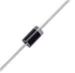
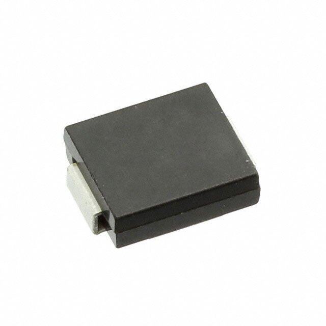
| 产品图片 |
|
| rohs | 符合RoHS无铅 / 符合限制有害物质指令(RoHS)规范要求 |
| 产品系列 | 二极管与整流器,整流器,ON Semiconductor 1N4933RLG- |
| 数据手册 | |
| 产品型号 | 1N4933RLG |
| 不同If时的电压-正向(Vf) | 1.2V @ 1A |
| 不同 Vr、F时的电容 | - |
| 不同 Vr时的电流-反向漏电流 | 5µA @ 50V |
| 二极管类型 | 标准 |
| 产品 | Fast Recovery Rectifiers |
| 产品目录页面 | |
| 产品种类 | 整流器 |
| 供应商器件封装 | DO-41 |
| 其它名称 | 1N4933RLGOSTR |
| 包装 | 带卷 (TR) |
| 反向恢复时间(trr) | 300ns |
| 反向电压 | 50 V |
| 反向电流IR | 5 uA |
| 商标 | ON Semiconductor |
| 安装类型 | 通孔 |
| 安装风格 | Through Hole |
| 封装 | Reel |
| 封装/外壳 | DO-204AL,DO-41,轴向 |
| 封装/箱体 | DO-41 |
| 工作温度-结 | -65°C ~ 150°C |
| 工厂包装数量 | 5000 |
| 恢复时间 | 300 ns |
| 最大工作温度 | + 150 C |
| 最大浪涌电流 | 30 A |
| 最小工作温度 | - 65 C |
| 标准包装 | 5,000 |
| 正向电压下降 | 1.2 V |
| 正向连续电流 | 1 A |
| 热阻 | 65°C/W Ja |
| 电压-DC反向(Vr)(最大值) | 50V |
| 电流-平均整流(Io) | 1A |
| 系列 | 1N4933 |
| 速度 | 快速恢复 =< 500 ns,> 200mA(Io) |
| 配置 | Single |


- 商务部:美国ITC正式对集成电路等产品启动337调查
- 曝三星4nm工艺存在良率问题 高通将骁龙8 Gen1或转产台积电
- 太阳诱电将投资9.5亿元在常州建新厂生产MLCC 预计2023年完工
- 英特尔发布欧洲新工厂建设计划 深化IDM 2.0 战略
- 台积电先进制程称霸业界 有大客户加持明年业绩稳了
- 达到5530亿美元!SIA预计今年全球半导体销售额将创下新高
- 英特尔拟将自动驾驶子公司Mobileye上市 估值或超500亿美元
- 三星加码芯片和SET,合并消费电子和移动部门,撤换高东真等 CEO
- 三星电子宣布重大人事变动 还合并消费电子和移动部门
- 海关总署:前11个月进口集成电路产品价值2.52万亿元 增长14.8%


PDF Datasheet 数据手册内容提取
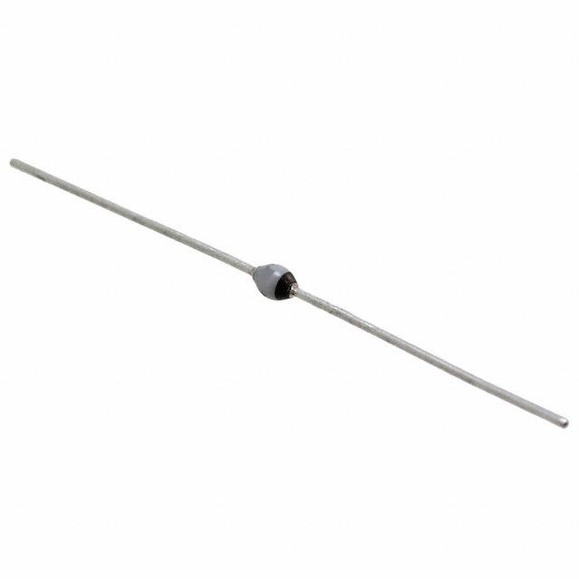
1N4933, 1N4934, 1N4935, 1N4936, 1N4937 Axial-Lead Glass Passivated Fast Recovery Rectifiers www.onsemi.com Axial−lead, fast−recovery rectifiers are designed for special applications such as DC power supplies, inverters, converters, ultrasonic systems, choppers, low RF interference and free wheeling FAST RECOVERY RECTIFIERS diodes. A complete line of fast recovery rectifiers having typical recovery time of 150 nanoseconds providing high efficiency at 1.0 AMPERE, 50−600 VOLTS frequencies to 250 kHz. Features • Shipped in Plastic Bags; 1,000 per Bag • Available Tape and Reeled; 5,000 per Reel, by Adding a “RL” Suffix to the Part Number • These are Pb−Free Devices* Mechanical Characteristics: • Case: Epoxy, Molded AXIAL LEAD • Weight: 0.4 Gram (Approximately) CASE 59 • STYLE 1 Finish: All External Surfaces Corrosion Resistant and Terminal Leads are Readily Solderable • Lead Temperature for Soldering Purposes: 260°C Max. for 10 Seconds • Polarity: Cathode Indicated by Polarity Band MARKING DIAGRAM *For additional information on our Pb−Free strategy and soldering details, please download the ON Semiconductor Soldering and Mounting Techniques A Reference Manual, SOLDERRM/D. 1N493x YYWW(cid:2) (cid:2) A =Assembly Location 1N493x =Device Number x= 3, 4, 5, 6 or 7 YY =Year WW =Work Week (cid:2) =Pb−Free Package (Note: Microdot may be in either location) ORDERING INFORMATION See detailed ordering and shipping information on page 3 of this data sheet. © Semiconductor Components Industries, LLC, 2006 1 Publication Order Number: June, 2018 − Rev. 13 1N4933/D
1N4933, 1N4934, 1N4935, 1N4936, 1N4937 MAXIMUM RATINGS (Note 1) Rating Symbol 1N4933 1N4934 1N4935 1N4936 1N4937 Unit †Peak Repetitive Reverse Voltage VRRM 50 100 200 400 600 V Working Peak Reverse Voltage VRWM DC Blocking Voltage VR †Non−Repetitive Peak Reverse Voltage VRSM 75 150 250 450 650 V RMS Reverse Voltage VR(RMS) 35 70 140 280 420 †Average Rectified Forward Current IO 1.0 A (Single phase, resistive load, TA = 75°C) (Note 2) †Non−Repetitive Peak Surge Current IFSM 30 A (Surge applied at rated load conditions) Operating Junction Temperature Range TJ, Tstg −65 to +150 °C Storage Temperature Range Stresses exceeding those listed in the Maximum Ratings table may damage the device. If any of these limits are exceeded, device functionality should not be assumed, damage may occur and reliability may be affected. 1. Ratings at 25°C ambient temperature unless otherwise specified. 2. Derate by 20% for capacitive loads. THERMAL CHARACTERISTICS Characteristic Symbol Max Unit Thermal Resistance, Junction−to−Ambient (Typical Printed Circuit Board Mounting) R(cid:2)JA 65 °C/W ELECTRICAL CHARACTERISTICS Characteristic Symbol Min Typ Max Unit Instantaneous Forward Voltage (IF = 3.14 Amp, TJ = 150°C) vF − 1.0 1.2 V Forward Voltage (IF = 1.0 Amp, TA = 25°C) VF − 1.05 1.2 V †Reverse Current (Rated DC Voltage) TA = 25°C IR − 1.0 5.0 (cid:3)A TA = 100°C − 50 100 REVERSE RECOVERY CHARACTERISTICS† Reverse Recovery Time (IF = 1.0 Amp to VR = 30 Vdc) trr − 150 200 ns (IFM = 15 Amp, di/dt = 10 A/(cid:3)s) − 175 300 Reverse Recovery Current (IF = 1.0 Amp to VR = 30 Vdc) IRM(REC) − 1.0 2.0 A Product parametric performance is indicated in the Electrical Characteristics for the listed test conditions, unless otherwise noted. Product performance may not be indicated by the Electrical Characteristics if operated under different conditions. †Indicates JEDEC Registered Data for 1N4933 Series. 10 1.0E−03 TC = 150°C NT (A) T (A)1.0E−04 TC = 125°C E N R E UR RR1.0E−05 TC = 100°C WARD C 1 TC = 12T5C° C= 150°C RSE CU1.0E−06 E OR TC = 100°C EV F R I, F I, R1.0E−07 TC = 25°C TC = 25°C 0.1 1.0E−08 0.4 0.6 0.8 1 1.2 1.4 0 100 200 300 400 500 600 VF, INSTANTANEOUS FORWARD VOLTAGE (V) VR, REVERSE VOLTAGE (V) Figure 1. Typical Forward Voltage Figure 2. Typical Reverse Current www.onsemi.com 2
1N4933, 1N4934, 1N4935, 1N4936, 1N4937 10 TJ = 25°C T (A) 11..86 (cid:2)JA = 65°C/W N E F) RR 1.4 p U CE ( D C 1.2 N R 1.0 DC A A T W CI R 0.8 A O P F CA E 0.6 C, AG 0.4 R E V 0.2 A 1 , O 0 0 20 40 60 80 100 120 140 160 180 200 I 0 20 40 60 80 100 120 140 160 VR, REVERSE VOLTAGE (V) TA, AMBIENT TEMPERATURE (C) Figure 3. Typical Capacitance Figure 4. Current Derating ORDERING INFORMATION Device Package Shipping† 1N4933 Axial Lead* 1000 Units / Bag 1N4933G Axial Lead* 1000 Units / Bag 1N4933RL Axial Lead* 5000 / Tape & Reel 1N4933RLG Axial Lead* 5000 / Tape & Reel 1N4934 Axial Lead* 1000 Units / Bag 1N4934G Axial Lead* 1000 Units / Bag 1N4934RL Axial Lead* 5000 / Tape & Reel 1N4934RLG Axial Lead* 5000 / Tape & Reel 1N4935 Axial Lead* 1000 Units / Bag 1N4935G Axial Lead* 1000 Units / Bag 1N4935RL Axial Lead* 5000 / Tape & Reel 1N4935RLG Axial Lead* 5000 / Tape & Reel 1N4936 Axial Lead* 1000 Units / Bag 1N4936G Axial Lead* 1000 Units / Bag 1N4936RL Axial Lead* 5000 / Tape & Reel 1N4936RLG Axial Lead* 5000 / Tape & Reel 1N4937 Axial Lead* 1000 Units / Bag 1N4937G Axial Lead* 1000 Units / Bag 1N4937RL Axial Lead* 5000 / Tape & Reel 1N4937RLG Axial Lead* 5000 / Tape & Reel †For information on tape and reel specifications, including part orientation and tape sizes, please refer to our Tape and Reel Packaging Specifications Brochure, BRD8011/D. *This package is inherently Pb−Free. www.onsemi.com 3
1N4933, 1N4934, 1N4935, 1N4936, 1N4937 PACKAGE DIMENSIONS AXIAL LEAD CASE 59−10 ISSUE U NOTES: 1. DIMENSIONING AND TOLERANCING PER ANSI B Y14.5M, 1982. 2. CONTROLLING DIMENSION: INCH. 3. ALL RULES AND NOTES ASSOCIATED WITH JEDEC DO−41 OUTLINE SHALL APPLY 4. POLARITY DENOTED BY CATHODE BAND. 5. LEAD DIAMETER NOT CONTROLLED WITHIN F DIMENSION. K D INCHES MILLIMETERS DIM MIN MAX MIN MAX F A 0.161 0.205 4.10 5.20 B 0.079 0.106 2.00 2.70 D 0.028 0.034 0.71 0.86 A F −−− 0.050 −−− 1.27 K 1.000 −−− 25.40 −−− POLARITY INDICATOR OPTIONAL AS NEEDED F STYLE 1: (SEE STYLES) PIN 1.CATHODE (POLARITY BAND) 2.ANODE K ON Semiconductor and are trademarks of Semiconductor Components Industries, LLC dba ON Semiconductor or its subsidiaries in the United States and/or other countries. ON Semiconductor owns the rights to a number of patents, trademarks, copyrights, trade secrets, and other intellectual property. A listing of ON Semiconductor’s product/patent coverage may be accessed at www.onsemi.com/site/pdf/Patent−Marking.pdf. ON Semiconductor reserves the right to make changes without further notice to any products herein. ON Semiconductor makes no warranty, representation or guarantee regarding the suitability of its products for any particular purpose, nor does ON Semiconductor assume any liability arising out of the application or use of any product or circuit, and specifically disclaims any and all liability, including without limitation special, consequential or incidental damages. Buyer is responsible for its products and applications using ON Semiconductor products, including compliance with all laws, regulations and safety requirements or standards, regardless of any support or applications information provided by ON Semiconductor. “Typical” parameters which may be provided in ON Semiconductor data sheets and/or specifications can and do vary in different applications and actual performance may vary over time. All operating parameters, including “Typicals” must be validated for each customer application by customer’s technical experts. ON Semiconductor does not convey any license under its patent rights nor the rights of others. ON Semiconductor products are not designed, intended, or authorized for use as a critical component in life support systems or any FDA Class 3 medical devices or medical devices with a same or similar classification in a foreign jurisdiction or any devices intended for implantation in the human body. Should Buyer purchase or use ON Semiconductor products for any such unintended or unauthorized application, Buyer shall indemnify and hold ON Semiconductor and its officers, employees, subsidiaries, affiliates, and distributors harmless against all claims, costs, damages, and expenses, and reasonable attorney fees arising out of, directly or indirectly, any claim of personal injury or death associated with such unintended or unauthorized use, even if such claim alleges that ON Semiconductor was negligent regarding the design or manufacture of the part. ON Semiconductor is an Equal Opportunity/Affirmative Action Employer. This literature is subject to all applicable copyright laws and is not for resale in any manner. PUBLICATION ORDERING INFORMATION LITERATURE FULFILLMENT: N. American Technical Support: 800−282−9855 Toll Free ON Semiconductor Website: www.onsemi.com Literature Distribution Center for ON Semiconductor USA/Canada 19521 E. 32nd Pkwy, Aurora, Colorado 80011 USA Europe, Middle East and Africa Technical Support: Order Literature: http://www.onsemi.com/orderlit Phone: 303−675−2175 or 800−344−3860 Toll Free USA/Canada Phone: 421 33 790 2910 Fax: 303−675−2176 or 800−344−3867 Toll Free USA/Canada For additional information, please contact your local Email: orderlit@onsemi.com Sales Representative ◊ www.onsemi.com 1N4933/D 4