ICGOO在线商城 > 分立半导体产品 > 二极管 - 整流器 - 单 > 1N4002RLG
 Datasheet下载
- 型号: 1N4002RLG
- 制造商: ON Semiconductor
- 库位|库存: xxxx|xxxx
- 要求:
| 数量阶梯 | 香港交货 | 国内含税 |
| +xxxx | $xxxx | ¥xxxx |
查看当月历史价格
查看今年历史价格
1N4002RLG产品简介:
ICGOO电子元器件商城为您提供1N4002RLG由ON Semiconductor设计生产,在icgoo商城现货销售,并且可以通过原厂、代理商等渠道进行代购。 1N4002RLG价格参考。ON Semiconductor1N4002RLG封装/规格:二极管 - 整流器 - 单, 标准 通孔 二极管 100V 1A DO-41。您可以下载1N4002RLG参考资料、Datasheet数据手册功能说明书,资料中有1N4002RLG 详细功能的应用电路图电压和使用方法及教程。
1N4002RLG是ON Semiconductor公司生产的二极管,属于整流器单二极管系列。该型号主要用于电力电子电路中的整流、滤波和平滑等应用场景。以下是其主要应用领域和特点:

 1. 电源整流
1N4002RLG常用于将交流电(AC)转换为直流电(DC)的整流电路中。它能够承受最大反向电压为100V,正向电流为1A,适合应用于低压、小电流的整流场合,如小型开关电源、线性电源等。

 2. 保护电路
该二极管还可以用作保护元件,防止电路中的瞬态电压或反向电流对敏感器件造成损害。例如,在电机驱动电路中,它可以吸收感性负载产生的反电动势,保护晶体管或其他半导体器件免受损坏。

 3. 续流二极管
在开关电源、逆变器和变频器等电路中,1N4002RLG可以作为续流二极管使用。当开关元件(如MOSFET或IGBT)关断时,它能够提供一个路径让电感中的电流继续流通,避免电流突然中断导致的电压尖峰。

 4. 浪涌抑制
1N4002RLG具有较好的浪涌耐受能力,能够在短时间内承受较大的电流冲击。因此,它可以在一些需要应对短时大电流冲击的应用中使用,如汽车电子设备中的电源电路。

 5. 低功耗设备
由于1N4002RLG的工作电压和电流相对较低,它非常适合用于低功耗设备,如便携式电子产品、电池供电设备等。这些设备通常要求二极管具有较小的正向压降和较低的功耗,以延长电池寿命。

 6. 信号隔离
在某些通信或控制电路中,1N4002RLG可以用作信号隔离元件,确保不同部分的电路之间不会相互干扰。它能够有效地阻隔反向信号,同时允许正向信号通过。

总之,1N4002RLG是一款通用性强、性能稳定的整流二极管,适用于多种电力电子应用场合,尤其是在低压、小电流的整流和保护电路中表现尤为出色。
| 参数 | 数值 |
| 产品目录 | |
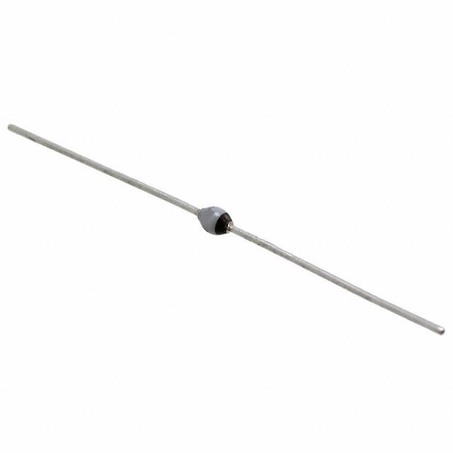
| 描述 | DIODE GEN PURPOSE 100V 1A DO41整流器 100V 1A Standard |
| 产品分类 | 单二极管/整流器分离式半导体 |
| 品牌 | ON Semiconductor |
| 产品手册 | |
| 产品图片 |
|
| rohs | 符合RoHS无铅 / 符合限制有害物质指令(RoHS)规范要求 |
| 产品系列 | 二极管与整流器,整流器,ON Semiconductor 1N4002RLG- |
| 数据手册 | |
| 产品型号 | 1N4002RLG |
| 不同If时的电压-正向(Vf) | 1.1V @ 1A |
| 不同 Vr、F时的电容 | - |
| 不同 Vr时的电流-反向漏电流 | 10µA @ 100V |
| 二极管类型 | 标准 |
| 产品 | Standard Recovery Rectifiers |
| 产品种类 | 整流器 |
| 供应商器件封装 | DO-41 |
| 其它名称 | 1N4002RLGOSTR |
| 包装 | 带卷 (TR) |
| 反向恢复时间(trr) | - |
| 反向电压 | 100 V |
| 反向电流IR | 10 uA |
| 商标 | ON Semiconductor |
| 安装类型 | 通孔 |
| 安装风格 | Through Hole |
| 封装 | Reel |
| 封装/外壳 | DO-204AL,DO-41,轴向 |
| 封装/箱体 | DO-41 |
| 工作温度-结 | -65°C ~ 175°C |
| 工厂包装数量 | 5000 |
| 最大工作温度 | + 175 C |
| 最大浪涌电流 | 30 A |
| 最小工作温度 | - 65 C |
| 标准包装 | 5,000 |
| 正向电压下降 | 1.1 V |
| 正向连续电流 | 1 A |
| 热阻 | 52°C/W Ja |
| 电压-DC反向(Vr)(最大值) | 100V |
| 电流-平均整流(Io) | 1A |
| 系列 | 1N4002 |
| 速度 | 标准恢复 >500ns,> 200mA(Io) |
| 配置 | Single |


PDF Datasheet 数据手册内容提取
1N4001, 1N4002, 1N4003, 1N4004, 1N4005, 1N4006, 1N4007 Axial-Lead Glass Passivated Standard Recovery Rectifiers www.onsemi.com This data sheet provides information on subminiature size, axial lead mounted rectifiers for general−purpose low−power applications. LEAD MOUNTED RECTIFIERS 50−1000 VOLTS Features • DIFFUSED JUNCTION Shipped in Plastic Bags, 1000 per bag • Available Tape and Reeled, 5000 per reel, by adding a “RL” suffix to the part number • Available in Fan−Fold Packaging, 3000 per box, by adding a “FF” suffix to the part number • Pb−Free Packages are Available Mechanical Characteristics • Case: Epoxy, Molded • CASE 59−10 Weight: 0.4 gram (approximately) • AXIAL LEAD Finish: All External Surfaces Corrosion Resistant and Terminal PLASTIC Leads are Readily Solderable • Lead and Mounting Surface Temperature for Soldering Purposes: 260°C Max. for 10 Seconds, 1/16 in. from case • Polarity: Cathode Indicated by Polarity Band MARKING DIAGRAM *For additional information on our Pb−Free strategy and soldering details, please download the ON Semiconductor Soldering and Mounting Techniques A Reference Manual, SOLDERRM/D. 1N400x YYWW(cid:2) (cid:2) A = Assembly Location 1N400x= Device Number x = 1, 2, 3, 4, 5, 6 or 7 YY = Year WW = Work Week (cid:2) = Pb−Free Package (Note: Microdot may be in either location) ORDERING INFORMATION See detailed ordering and shipping information on page 5 of this data sheet. © Semiconductor Components Industries, LLC, 2012 1 Publication Order Number: June, 2018 − Rev. 14 1N4001/D
1N4001, 1N4002, 1N4003, 1N4004, 1N4005, 1N4006, 1N4007 MAXIMUM RATINGS Rating Symbol 1N4001 1N4002 1N4003 1N4004 1N4005 1N4006 1N4007 Unit †Peak Repetitive Reverse Voltage VRRM 50 100 200 400 600 800 1000 V Working Peak Reverse Voltage VRWM DC Blocking Voltage VR †Non−Repetitive Peak Reverse Voltage VRSM 60 120 240 480 720 1000 1200 V (halfwave, single phase, 60 Hz) †RMS Reverse Voltage VR(RMS) 35 70 140 280 420 560 700 V †Average Rectified Forward Current IO 1.0 A (single phase, resistive load, 60 Hz, TA = 75°C) †Non−Repetitive Peak Surge Current IFSM 30 (for 1 cycle) A (surge applied at rated load conditions) Operating and Storage Junction TJ −65 to +175 °C Temperature Range Tstg Stresses exceeding those listed in the Maximum Ratings table may damage the device. If any of these limits are exceeded, device functionality should not be assumed, damage may occur and reliability may be affected. †Indicates JEDEC Registered Data THERMAL CHARACTERISTICS Rating Symbol Max Unit Maximum Thermal Resistance, Junction−to−Ambient R(cid:2)JA Note 1 °C/W ELECTRICAL CHARACTERISTICS† Rating Symbol Typ Max Unit Maximum Instantaneous Forward Voltage Drop, (iF = 1.0 Amp, TJ = 25°C) vF 0.93 1.1 V Maximum Full−Cycle Average Forward Voltage Drop, (IO = 1.0 Amp, TL = 75°C, 1 inch leads) VF(AV) − 0.8 V Maximum Reverse Current (rated DC voltage) IR (cid:3)A (TJ = 25°C) 0.05 10 (TJ = 100°C) 1.0 50 Maximum Full−Cycle Average Reverse Current, (IO = 1.0 Amp, TL = 75°C, 1 inch leads) IR(AV) − 30 (cid:3)A Product parametric performance is indicated in the Electrical Characteristics for the listed test conditions, unless otherwise noted. Product performance may not be indicated by the Electrical Characteristics if operated under different conditions. †Indicates JEDEC Registered Data www.onsemi.com 2
1N4001, 1N4002, 1N4003, 1N4004, 1N4005, 1N4006, 1N4007 10 1.0E−04 NT (A) T (A)1.0E−05 TC = 150°C E N R E R R D CU 1 TC = 100°C CUR1.0E−06 TC = 100°C R E WA RS1.0E−07 R E FO TC = 150°C REV I, F TC = 25°C I, R1.0E−08 TC = 25°C 0.1 1.0E−09 0.5 0.6 0.7 0.8 0.9 1 1.1 1.2 0 100 200 300 400 500 600 700 800 9001000 VF, INSTANTANEOUS FORWARD VOLTAGE (V) VR, REVERSE VOLTAGE (V) Figure 1. Typical Forward Voltage Figure 2. Typical Reverse Current 100 TJ = 25°C F) p E ( C N TA 10 CI A P A C C, 1 0 20 40 60 80 100 120 140 160 180 200 VR, REVERSE VOLTAGE (V) Figure 3. Typical Capacitance www.onsemi.com 3
1N4001, 1N4002, 1N4003, 1N4004, 1N4005, 1N4006, 1N4007 NOTE 1. − AMBIENT MOUNTING DATA Data shown for thermal resistance, junction−to−ambient (R(cid:2)JA) for the mountings shown is to be used as typical guideline values for preliminary engineering or in case the tie point temperature cannot be measured. TYPICAL VALUES FOR R(cid:2)JA IN STILL AIR Mounting Lead Length, L Method 1/8 1/4 1/2 Units 1 52 65 72 °C/W 2 R(cid:2)JA 67 80 87 °C/W 3 50 °C/W MOUNTING METHOD 1 L L ÉÉÉÉÉÉÉÉÉÉÉ ÉÉÉÉÉÉÉÉÉÉÉ MOUNTING METHOD 2 L L ÉÉÉÉÉÉÉÉÉÉÉÉ ÉÉÉÉÉÉÉÉÉÉÉÉ Vector Pin Mounting MOUNTING METHOD 3 ÉÉ ÉÉ L = 3/8″ ÉÉ ÉÉ ÉÉ ÉÉ Board Ground Plane ÉÉ P.C. Board with 1−1/2 ″ X 1−1/2 ″ Copper Surface www.onsemi.com 4
1N4001, 1N4002, 1N4003, 1N4004, 1N4005, 1N4006, 1N4007 ORDERING INFORMATION Device Package Shipping† 1N4001 Axial Lead* 1000 Units/Bag 1N4001G Axial Lead* 1000 Units/Bag (Pb−Free) 1N4001FF Axial Lead* 3000 Units/Box 1N4001FFG Axial Lead* 3000 Units/Box (Pb−Free) 1N4001RL Axial Lead* 5000/Tape & Reel 1N4001RLG Axial Lead* 5000/Tape & Reel (Pb−Free) 1N4002 Axial Lead* 1000 Units/Bag 1N4002G Axial Lead* 1000 Units/Bag (Pb−Free) 1N4002FF Axial Lead* 3000 Units/Box 1N4002FFG Axial Lead* 3000 Units/Box (Pb−Free) 1N4002RL Axial Lead* 5000/Tape & Reel 1N4002RLG Axial Lead* 5000/Tape & Reel (Pb−Free) 1N4003 Axial Lead* 1000 Units/Bag 1N4003G Axial Lead* 1000 Units/Bag (Pb−Free) 1N4003FF Axial Lead* 3000 Units/Box 1N4003FFG Axial Lead* 3000 Units/Box (Pb−Free) 1N4003RL Axial Lead* 5000/Tape & Reel 1N4003RLG Axial Lead* 5000/Tape & Reel (Pb−Free) 1N4004 Axial Lead* 1000 Units/Bag 1N4004G Axial Lead* 1000 Units/Bag (Pb−Free) 1N4004FF Axial Lead* 3000 Units/Box 1N4004FFG Axial Lead* 3000 Units/Box (Pb−Free) 1N4004RL Axial Lead* 5000/Tape & Reel 1N4004RLG Axial Lead* 5000/Tape & Reel (Pb−Free) 1N4005 Axial Lead* 1000 Units/Bag 1N4005G Axial Lead* 1000 Units/Bag (Pb−Free) 1N4005FF Axial Lead* 3000 Units/Box 1N4005FFG Axial Lead* 3000 Units/Box (Pb−Free) 1N4005RL Axial Lead* 5000/Tape & Reel 1N4005RLG Axial Lead* 5000/Tape & Reel (Pb−Free) †For information on tape and reel specifications, including part orientation and tape sizes, please refer to our Tape and Reel Packaging Specifications Brochure, BRD8011/D. *This package is inherently Pb−Free. www.onsemi.com 5
1N4001, 1N4002, 1N4003, 1N4004, 1N4005, 1N4006, 1N4007 ORDERING INFORMATION Device Package Shipping† 1N4006 Axial Lead* 1000 Units/Bag 1N4006G Axial Lead* 1000 Units/Bag (Pb−Free) 1N4006FF Axial Lead* 3000 Units/Box 1N4006FFG Axial Lead* 3000 Units/Box (Pb−Free) 1N4006RL Axial Lead* 5000/Tape & Reel 1N4006RLG Axial Lead* 5000/Tape & Reel (Pb−Free) 1N4007 Axial Lead* 1000 Units/Bag 1N4007G Axial Lead* 1000 Units/Bag (Pb−Free) 1N4007FF Axial Lead* 3000 Units/Box 1N4007FFG Axial Lead* 3000 Units/Box (Pb−Free) 1N4007RL Axial Lead* 5000/Tape & Reel 1N4007RLG Axial Lead* 5000/Tape & Reel (Pb−Free) †For information on tape and reel specifications, including part orientation and tape sizes, please refer to our Tape and Reel Packaging Specifications Brochure, BRD8011/D. *This package is inherently Pb−Free. www.onsemi.com 6
1N4001, 1N4002, 1N4003, 1N4004, 1N4005, 1N4006, 1N4007 PACKAGE DIMENSIONS AXIAL LEAD CASE 59−10 ISSUE U B NOTES: 1. DIMENSIONING AND TOLERANCING PER ANSI Y14.5M, 1982. 2. CONTROLLING DIMENSION: INCH. K D 3. ALL RULES AND NOTES ASSOCIATED WITH JEDEC DO−41 OUTLINE SHALL APPLY 4. POLARITY DENOTED BY CATHODE BAND. F 5. LEAD DIAMETER NOT CONTROLLED WITHIN F DIMENSION. A INCHES MILLIMETERS DIM MIN MAX MIN MAX A 0.161 0.205 4.10 5.20 OPPOTLIOANRAITLY A INS DNICEEADTOERD F B 0.079 0.106 2.00 2.70 (SEE STYLES) D 0.028 0.034 0.71 0.86 F −−− 0.050 −−− 1.27 K K 1.000 −−− 25.40 −−− ON Semiconductor and are trademarks of Semiconductor Components Industries, LLC dba ON Semiconductor or its subsidiaries in the United States and/or other countries. ON Semiconductor owns the rights to a number of patents, trademarks, copyrights, trade secrets, and other intellectual property. A listing of ON Semiconductor’s product/patent coverage may be accessed at www.onsemi.com/site/pdf/Patent−Marking.pdf. ON Semiconductor reserves the right to make changes without further notice to any products herein. ON Semiconductor makes no warranty, representation or guarantee regarding the suitability of its products for any particular purpose, nor does ON Semiconductor assume any liability arising out of the application or use of any product or circuit, and specifically disclaims any and all liability, including without limitation special, consequential or incidental damages. Buyer is responsible for its products and applications using ON Semiconductor products, including compliance with all laws, regulations and safety requirements or standards, regardless of any support or applications information provided by ON Semiconductor. “Typical” parameters which may be provided in ON Semiconductor data sheets and/or specifications can and do vary in different applications and actual performance may vary over time. All operating parameters, including “Typicals” must be validated for each customer application by customer’s technical experts. ON Semiconductor does not convey any license under its patent rights nor the rights of others. ON Semiconductor products are not designed, intended, or authorized for use as a critical component in life support systems or any FDA Class 3 medical devices or medical devices with a same or similar classification in a foreign jurisdiction or any devices intended for implantation in the human body. Should Buyer purchase or use ON Semiconductor products for any such unintended or unauthorized application, Buyer shall indemnify and hold ON Semiconductor and its officers, employees, subsidiaries, affiliates, and distributors harmless against all claims, costs, damages, and expenses, and reasonable attorney fees arising out of, directly or indirectly, any claim of personal injury or death associated with such unintended or unauthorized use, even if such claim alleges that ON Semiconductor was negligent regarding the design or manufacture of the part. ON Semiconductor is an Equal Opportunity/Affirmative Action Employer. This literature is subject to all applicable copyright laws and is not for resale in any manner. PUBLICATION ORDERING INFORMATION LITERATURE FULFILLMENT: N. American Technical Support: 800−282−9855 Toll Free ON Semiconductor Website: www.onsemi.com Literature Distribution Center for ON Semiconductor USA/Canada 19521 E. 32nd Pkwy, Aurora, Colorado 80011 USA Europe, Middle East and Africa Technical Support: Order Literature: http://www.onsemi.com/orderlit Phone: 303−675−2175 or 800−344−3860 Toll Free USA/Canada Phone: 421 33 790 2910 Fax: 303−675−2176 or 800−344−3867 Toll Free USA/Canada For additional information, please contact your local Email: orderlit@onsemi.com Sales Representative ◊ www.onsemi.com 1N4001/D 7
Mouser Electronics Authorized Distributor Click to View Pricing, Inventory, Delivery & Lifecycle Information: O N Semiconductor: 1N4001 1N4001FF 1N4001FFG 1N4001G 1N4001RL 1N4001RLG 1N4002 1N4002FF 1N4002FFG 1N4002G 1N4002RL 1N4002RLG 1N4003 1N4003FF 1N4003FFG 1N4003G 1N4003RL 1N4003RLG 1N4004 1N4004FF 1N4004FFG 1N4004G 1N4004RL 1N4004RLG 1N4005 1N4005FF 1N4005FFG 1N4005G 1N4005RL 1N4005RLG 1N4006 1N4006FF 1N4006FFG 1N4006G 1N4006RL 1N4006RLG 1N4007 1N4007FF 1N4007FFG 1N4007G 1N4007RL 1N4007RLG