ICGOO在线商城 > 100-1241-1
 Datasheet下载
- 型号: 100-1241-1
- 制造商: Bluetechnix
- 库位|库存: xxxx|xxxx
- 要求:
| 数量阶梯 | 香港交货 | 国内含税 |
| +xxxx | $xxxx | ¥xxxx |
查看当月历史价格
查看今年历史价格
100-1241-1产品简介:
ICGOO电子元器件商城为您提供100-1241-1由Bluetechnix设计生产,在icgoo商城现货销售,并且可以通过原厂、代理商等渠道进行代购。 提供100-1241-1价格参考以及Bluetechnix100-1241-1封装/规格参数等产品信息。 你可以下载100-1241-1参考资料、Datasheet数据手册功能说明书, 资料中有100-1241-1详细功能的应用电路图电压和使用方法及教程。
| 参数 | 数值 |
| CacheMemory | 32 MB |
| 品牌 | Bluetechnix |
| 产品目录 | 嵌入式解决方案 |
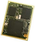
| 描述 | 模块化系统 - SOM CM-BF548-C-C Q25S64F8 |
| 产品分类 | 计算 |
| 产品手册 | |
| 产品图片 |
|
| rohs | 符合RoHS |
| 产品系列 | 模块化系统 - SOM,Bluetechnix 100-1241-1 |
| mouser_ship_limit | 该产品可能需要其他文件才能进口到中国。 |
| 产品型号 | 100-1241-1 |
| 产品种类 | 模块化系统 - SOM |
| 商标 | Bluetechnix |
| 处理器类型 | ADSP-BF548BBCZ-5X |
| 备用电池 | No |
| 外观尺寸 | - |
| 存储容量 | 8 MB |
| 存储类型 | NAND Flash, DDR-SDRAM |
| 封装 | Reel |
| 尺寸 | 41 mm x 28.5 mm x 3 mm |
| 工作电源电压 | 3.3 V |
| 工厂包装数量 | 50 |
| 接口类型 | CAN, SPI, UART, USB |
| 最大工作温度 | + 85 C |
| 最小工作温度 | - 40 C |
| 系列 | Blackfin |
| 闪光 | 8 MB |
| 频率 | 533 MHz |


- 商务部:美国ITC正式对集成电路等产品启动337调查
- 曝三星4nm工艺存在良率问题 高通将骁龙8 Gen1或转产台积电
- 太阳诱电将投资9.5亿元在常州建新厂生产MLCC 预计2023年完工
- 英特尔发布欧洲新工厂建设计划 深化IDM 2.0 战略
- 台积电先进制程称霸业界 有大客户加持明年业绩稳了
- 达到5530亿美元!SIA预计今年全球半导体销售额将创下新高
- 英特尔拟将自动驾驶子公司Mobileye上市 估值或超500亿美元
- 三星加码芯片和SET,合并消费电子和移动部门,撤换高东真等 CEO
- 三星电子宣布重大人事变动 还合并消费电子和移动部门
- 海关总署:前11个月进口集成电路产品价值2.52万亿元 增长14.8%


PDF Datasheet 数据手册内容提取
Hardware User Manual CM-BF548 V1.x
Contact Bluetechnix Mechatronische Systeme GmbH Lainzerstraße 162/3 A-1130 Vienna AUSTRIA/EUROPE office@bluetechnix.at http://www.bluetechnix.com Document No.: 100-1241-1.0 Document Revision 13 Date: 2010-02-02 Blackfin CM-BF548 Hardware User Manual 1
Table of Contents 1 Introduction .................................................................................................................................................................................. 8 1.1 Overview ............................................................................................................................................................................... 8 1.2 Key Features ........................................................................................................................................................................ 9 1.3 Target Applications ........................................................................................................................................................... 9 1.4 Further Information .......................................................................................................................................................... 9 2 Specification .............................................................................................................................................................................. 10 2.1 Functional Specification ............................................................................................................................................... 10 2.2 Boot Mode ......................................................................................................................................................................... 10 2.3 Memory Map .................................................................................................................................................................... 11 2.3.1 Core Module Memory .......................................................................................................................................... 11 2.3.2 Externally Addressable Memory Space (on connector) ........................................................................... 11 2.4 Electrical Specification .................................................................................................................................................. 11 2.4.1 Supply Voltage ....................................................................................................................................................... 11 2.4.2 Supply Voltage Ripple ......................................................................................................................................... 11 2.4.3 Oscillator Frequency ............................................................................................................................................ 11 2.4.4 Supply Current ....................................................................................................................................................... 11 2.5 Environmental Specification ....................................................................................................................................... 12 2.5.1 Temperature ........................................................................................................................................................... 12 2.5.2 Humidity ................................................................................................................................................................... 12 3 CM-BF548 .................................................................................................................................................................................... 12 3.1 Mechanical Outline ........................................................................................................................................................ 12 3.1.1 Footprint .................................................................................................................................................................. 13 3.2 Schematic Symbols (Signals of X1a and X1b) ....................................................................................................... 15 3.3 Connector X1a – (1-100) ............................................................................................................................................... 16 3.4 Connector X1b – (101-200) .......................................................................................................................................... 18 3.5 Reset circuit....................................................................................................................................................................... 20 4 Software Support ..................................................................................................................................................................... 20 4.1 BLACKSheep ..................................................................................................................................................................... 20 4.2 uClinux ............................................................................................................................................................................... 21 5 Application Examples ............................................................................................................................................................. 21 5.1 Sample Schematic .......................................................................................................................................................... 21 6 Anomalies ................................................................................................................................................................................... 23 7 Production Report.................................................................................................................................................................... 23 7.1 CM-BF548 (100-1241) .................................................................................................................................................... 23 Blackfin CM-BF548 Hardware User Manual 2
8 Product Changes ...................................................................................................................................................................... 23 9 Document Revision History .................................................................................................................................................. 24 A List of Figures and Tables ...................................................................................................................................................... 25 Blackfin CM-BF548 Hardware User Manual 3
Edition 2008-09 © Bluetechnix Mechatronische Systeme GmbH 2008 All Rights Reserved. The information herein is given to describe certain components and shall not be considered as a guarantee of characteristics. Terms of delivery and rights of technical change reserved. We hereby disclaim any warranties, including but not limited to warranties of non-infringement, regarding circuits, descriptions and charts stated herein. Bluetechnix makes and you receive no warranties or conditions, express, implied, statutory or in any communication with you. Bluetechnix specifically disclaims any implied warranty of merchantability or fitness for a particular purpose. Bluetechnix takes no liability for any damages and errors causing of the usage of this board. The user of this board is responsible by himself for the functionality of his application. He is allowed to use the board only if he has the qualification. More information is found in the General Terms and Conditions (AGB). Information For further information on technology, delivery terms and conditions and prices please contact Bluetechnix (http://www.bluetechnix.com). Warning Due to technical requirements components may contain dangerous substances. The Core Modules and development systems contain ESD (electrostatic discharge) sensitive devices. Electro-static charges readily accumulate on the human body and equipment and can discharge without detection. Permanent damage may occur on devices subjected to high-energy discharges. Proper ESD precautions are recommended to avoid performance degradation or loss of functionality. Unused Core Modules and Development Boards should be stored in the protective shipping Blackfin CM-BF548 Hardware User Manual 4
BLACKFIN Products Core Modules: CM-BF533: Blackfin Processor Module powered by Analog Devices' single core ADSP- BF533 processor; up to 600MHz, 32MB SDRAM, 2MB flash, 2x60 pin expansion connectors and a size of 36.5x31.5mm. CM-BF537E: Blackfin Processor Module powered by Analog Devices' single core ADSP- BF537 processor; up to 600MHz, 32MB SDRAM, 4MB flash, integrated TP10/100 Ethernet physical transceiver, 2x60 pin expansion connectors and a size of 36.5x31.5mm. CM-BF537U: Blackfin Processor Module powered by Analog Devices' single core ADSP- BF537 processor; up to 600MHz, 32MB SDRAM, 4MB flash, integrated USB 2.0 Device, 2x60 pin expansion connectors and a size of 36.5x31.5mm. TCM-BF537: Blackfin Processor Module powered by Analog Devices' single core ADSP- BF537 processor; up to 500MHz, 32MB SDRAM, 8MB flash, a size of 28x28mm, 2x60 pin expansion connectors, Ball Grid Array or Border Pads for reflow soldering, industrial temperature range -40°C to +85°C. CM-BF561: Blackfin Processor Module powered by Analog Devices' dual core ADSP- BF561 processor; up to 2x 600MHz, 64MB SDRAM, 8MB flash, 2x60 pin expansion connectors and a size of 36.5x31.5mm. CM-BF527: The new Blackfin Processor Module is powered by Analog Devices' single core ADSP-BF527 processor; key features are USB OTG 2.0 and Ethernet. The 2x60 pin expansion connectors are backwards compatible with other Core Modules. CM-BF548: The new Blackfin Processor Module is powered by Analog Devices' single core ADSP-BF548 processor; key features are 64MB DDR SD-RAM 2x100 pin expansion connectors. TCM-BF518: The new Core Module CM-BF518 is powered by Analog Devices' single core ADSP-BF518 processor; up to 400MHz, 32MB SDRAM, up to 8MB flash. The 2x60 pin expansion connectors are backwards compatible with other Core Modules. Development Boards: EVAL-BF5xx: Low cost Blackfin processor Evaluation Board with one socket for any Bluetechnix Blackfin Core Module. Additional interfaces are available, e.g. an SD-Card. DEV-BF5xxDA-Lite: Get ready to program and debug Bluetechnix Core Modules with this tiny development platform including an USB-Based Debug Agent. The DEV- BF5xxDA-Lite is a low cost starter development system including a VDSP++ Evaluation Software License. DEV-BF548-Lite: Low-cost development board with one socket for Bluetechnix CM-BF548 Core Module. Additional interfaces are available, e.g. an SD-Card, USB and Ethernet. Blackfin CM-BF548 Hardware User Manual 5
DEV-BF548DA-Lite: Get ready to program and debug Bluetechnix CM-BF548 Core Module with this tiny development platform including an USB-Based Debug Agent. The DEV-BF548DA-Lite is a low-cost starter development system including a VDSP++ Evaluation Software License. EXT-Boards: The following Extender Boards are available: EXT-BF5xx-AUDIO, EXT-BF5xx- VIDEO, EXT-BF5xx-CAM, EXT-BF5xx-EXP-TR, EXT-BF5xx-USB-ETH2, EXT- BF5xx-AD/DA, EXT-BF548-EXP and EXT-BF518-ETH. Furthermore, we offer the development of customized extender boards for our customers. Software Support: BLACKSheep: The BLACKSheep VDK is a multithreaded framework for the Blackfin processor family from Analog Devices that includes driver support for a variety of hardware extensions. It is based on the real-time VDK kernel included within the VDSP++ development environment. LabVIEW: LabVIEW embedded support for Bluetechnix Core Modules is done by Schmid-Engineering AG: http://www.schmid-engineering.ch uClinux: All the Core Modules are fully supported by uClinux. The required boot loader and uClinux can be downloaded from: http://blackfin.uClinux.org. Upcoming Products and Software Releases: Keep up-to-date with all the changes to the Bluetechnix product line and software updates at: http://www.bluetechnix.com . Software Support: BLACKSheep: The BLACKSheep VDK is a multithreaded framework for the Blackfin processor family from Analog Devices that includes driver support for a variety of hardware extensions. It is based on the real-time VDK kernel included within the VDSP++ development environment. LabVIEW: LabVIEW embedded support for Bluetechnix Core Modules is done by Schmid-Engineering AG: http://www.schmid-engineering.ch uClinux: All the Core Modules are fully supported by uClinux. The required boot loader and uClinux can be downloaded from: http://blackfin.uClinux.org. Upcoming Products and Software Releases: Keep up-to-date with all the changes to the Bluetechnix product line and software updates at: http://www.bluetechnix.com Blackfin CM-BF548 Hardware User Manual 6
BLACKFIN Design Service Based on more than five years of experience with Blackfin, Bluetechnix offers development assistance as well as custom design services and software development. Blackfin CM-BF548 Hardware User Manual 7
1 Introduction The CM-BF548 is a high performance and low power processor module incorporating Analog Devices Blackfin family of processors. Special feature is the fast DDR SDRAM memory bus and the many IO Interfaces available on two 100 pin connectors. The module allows easy integration into high demanding very space and power limited applications. 1.1 Overview The Core Module CM-BF548 consists of the following components: Figure 1-1: Main components of the CM-BF548 module Analog Devices Blackfin Processor ADSP-BF548 o ADSP-BF548BBCZ-5X with 533MHz* (* please see chapter 7.1 for the correct part number) o Note: ADSP BF54x Variants can be mounted upon request for higher volumes 64 MB DDR SDRAM o DDR SDRAM MT46V32M16BN-6IT (32Mx16, 512Mbit @ 2.5V) 8 MB of Byte Addressable Flash o PF48F2000P0XBQ0 (4Mx16, 64Mbit @ 3.3 V; all 8MByte addressable) o Additional flash memory can be connected through the expansion board as parallel Flash using asynchronous chip select lines or the NAND Flash interface, or as SPI flash. Blackfin CM-BF548 Hardware User Manual 8
Low Voltage Reset Circuit o Resets module if power supply goes below 2.93V for at least 140ms Dynamic Core Voltage Control o Core voltage can be adjusted by setting software registers on the Blackfin processor o Core voltage range: 0.8 – TBD Expansion Connector A – 100pins o Data Bus o Address Bus o Control Signals (Memory Control, Reset, Interrupt, Timer) o PC (0..13) SD-IO Signals, SPORT, GPIO o PJ (1..13) Atapi Signals, GPIO o PH (0..7) o ClkOUT, CLKBUF o USB-OTG o JTAG o Boot Mode Pins o Power Supply Expansion Connector B – 100pins o PA (0..15) Main functions: SPORT, GPIO, Timer o PB (0..14) Main functions: SPI, UART, I2C, GPIO, Timer o PD (0..15) Main functions: Host Port, SPORT, PPI0, PPI1, PPI2 o PE (0..15) Main functions: SPI, UART, I2C, PPI1, GPIO o PF(0..15) Main functions: PPI0, GPIO o PG(0..15) Main functions: CAN1,2 , PPI0, SPI, Host Port, GPIO 1.2 Key Features Allows quick prototyping of product that comes very close to the final design Reduces development costs, faster time to market Very cost effective for small and medium volumes 1.3 Target Applications Generic high performance signal processor module Automotive Applications GUI Based Web Appliances Robotics: Tiny processor module for mobile robots 1.4 Further Information Further information, and document updates are available on the product homepage: http://www.bluetechnix.com/goto/cm-bf548 Blackfin CM-BF548 Hardware User Manual 9
2 Specification ATTENTION: Please check the orientation of the Core Module. Insertion in the wrong orientation will cause damage! 2.1 Functional Specification Figure 2-1: CM-BF548 Detailed Block Diagram Figure 2-1 shows a detailed block diagram of the CM-BF548 module. Beside the DDR SD-RAM control pins the CM-BF548 has all other pins of the Blackfin processor at its two main 100 pin connectors. Dynamic voltage control allows reducing power consumption to a minimum adjusting the core voltage and the clock frequency dynamically in accordance to the required processing power. A low voltage reset circuit guarantees a power on reset and resets the system when the input voltage drops below 2.93V. 2.2 Boot Mode BMODE3---0 Description 0000 Idle---no boot 0001 Boot from 8- or 16-bit external flash memory 0010 Boot from 16-bit asynchronous FIFO 0011 Boot from serial SPI memory (EEPROM or flash) 0100 Boot from SPI host device 0101 Boot from serial TWI memory (EEPROM/flash) 0110 Boot from TWI host 0111 Boot from UART host 1000 Reserved Blackfin CM-BF548 Hardware User Manual 10
1001 Reserved 1010 Boot from (DDR) SDRAM 1011 Boot from OTP memory 1100 Reserved 1101 Boot from 8- or 16-bit NAND flash memory via NFC 1110 Boot from 16-Bit Host DMA 1111 Boot from 8-Bit Host DMA Table 2-1: Available Boot Modes for the CM-BF548 By default the Boot Mode is set to 0000 (BMODE0 = LOW, BMODE1 = LOW; BMODE2 = LOW, BMODE3 = LOW). Push BMODE PINS to high in order to change the boot mode. 2.3 Memory Map 2.3.1 Core Module Memory Memory Type Start Address End Address Size Comment FLASH 0x20000000 0x207FFFFF 8MB PF48F2000P0XBQ0 DDR SDRAM 0x00000000 0x03FFFFFF 64MB MT46V32M16BN‐6IT Table 2-2: Memory Map 2.3.2 Externally Addressable Memory Space (on connector) The core module has 3 banks of the Asynchronous Memory interface of the Blackfin processor available, this can be addressed via the following addresses. Async Memory Start Address End Address Size Comment Bank 1 0x24000000 0x2400FFFF 64K Use nAMS 1 2 0x28000000 0x2800FFFF 64K Use nAMS 2 3 0x2C000000 0x2C00FFFF 64K Use nAMS 3 Table 2-3: External Asynchronous Memory Mapping These memory banks can be used to access various memory mapped devices or peripherals. 2.4 Electrical Specification 2.4.1 Supply Voltage 3.3V DC +/-10% 2.4.2 Supply Voltage Ripple 100mV peak to peak 0-20 MHz 2.4.3 Oscillator Frequency 25MHz 2.4.4 Supply Current Maximum supply current: ca. 450mA Operating conditions: Blackfin CM-BF548 Hardware User Manual 11
o CPU running at 533MHz, Core Voltage 1.25V, DDR RAM 20% bandwidth utilization @ 130MHz: ca. 230mA o CPU running at 300MHz, Core Voltage 0.9V DDR RAM 20% bandwidth utilization @ 1xxMHz: ca. 155mA 2.5 Environmental Specification 2.5.1 Temperature Operating at full 533 MHz: -40 to + 85°C (* see chapter 7.1) 2.5.2 Humidity Operating: 10% to 90% (non condensing) 3 CM-BF548 3.1 Mechanical Outline All dimensions are given in millimeters! Figure 3-1: Mechanical outline (top view) Blackfin CM-BF548 Hardware User Manual 12
Figure 3-2: Mechanical outline (bottom view) Take 0.5mm as a tolerance for the border of the board since it is braked out from a multiboard panel and some additional rest may remain. Figure 3-3: Side View with Connectors Mounted The total minimum mounting height including receptacle at the motherboard is 7.5mm. 3.1.1 Footprint For the baseboard the following connectors have to be used. Part Baseboard Manufacturer Manufacturer Part No. X1a,X1b Hirose FX10A-100S/10-SV Receptacle Table 3-1: Baseboard connector types The Connectors on the CM-BF548 are of the following type: Part Core Module Manufacturer Manufacturer Part No. X1a,X1b Hirose FX10A-100P/10-SV Header Table 3-2: Module connector types Blackfin CM-BF548 Hardware User Manual 13
Figure 3-4: Recommended Footprint for Baseboard Design (top view) Figure 3-4 shows the footprint of the connector looking through the board. The RED Pads of the connectors are shown in top view as placed on the top layer of an application Board. The fixing holes on top-right and bottom-left can be omitted, if no shock lock is required. For the exact connector footprints please refer to the manufacturer homepage. Info: A Library of the Baseboard module for the Altium Designer 6.x can be obtained from Bluetechnix upon request. Blackfin CM-BF548 Hardware User Manual 14
3.2 Schematic Symbols (Signals of X1a and X1b) 1 134 101 151 A1 ATAPI_PDIAG PA0/TFS2 PG15/CAN1RX/TACI5 2 74 102 152 A2 PJ13/BGH or A25 PA1/DT2SEC/TMR4 PG14/CAN1TX 3 75 103 153 A3 PJ12/BG PA2/DT2PRI PG13/CAN0RX/TACI4 4 76 104 154 A4 PJ11/BR PA3/TSCLK2 PG12/CAN0TX 5 77 105 155 A5 PJ10/ATAPI_IORDY PA4/RFS2 PG11/SPI1SS/MTXON 6 78 106 156 A6 PJ9/ATAPI_INTRQ PA5/DR2SEC/TMR5 PG10/SPI1_MOSI 7 79 107 157 A7 PJ8/ATAPI_DMARQ PA6/DR2PRI PG9/SPI1_MISO 8 80 108 158 A8 PJ7/ATAPI_DMACKB PA7/RSCLK2/TACLK0 PG8/SPI1_SCLK 9 81 109 159 A9 PJ6/ATAPI_CS1B PA8/TFS3/TACLK1 PG7/SPI1SEL3/HOST_WR/PPI2_CLK 10 82 110 160 A10 PJ5/ATAPI_CS0B PA9/DT3SEC/TMR6 PG6/SPI1SEL2/HOST_RD/PPI2_FS1 11 83 111 161 A11 PJ4/ATAPI_DIOBW PA10/DT3PRI/TACLK2 PG5/SPI1SEL1/HOST_CE/PPI2_FS2/CZM 12 84 112 162 A12 PJ3/ATAPI_DIORB PA11/TSCLK3/TACLK3 PG4/PPI0_D17 13 85 113 163 A13 PJ2/ND_RB PA12/RFS3/TACLK4 PG3/PPI0_D16 14 86 114 164 A14 PJ1/ND_CE PA13/DR3SEC/TMR7/TACLK5 PG2/PPI0_FS2 15 115 165 A15 PA14/DR3PRI/TACLK6 PG1/PPI0_FS1 87 116 166 PC13/SD_CMD PA15/RSCLK3/TACLK7/TACI7 PG0/PPI0_CLK/TMRCLK 30 88 AMS1 PC12/SD_CLK 31 89 119 167 AMS2 PC11/SD_D3 PB0/SCL1 PF15/PPI0_D15 32 90 120 168 AMS3 PC10/SD_D2 PB1/SDA1 PF14/PPI0_D14 91 121 169 PC9/SD_D1 PB2/RTS3 PF13/PPI0_D13 16 92 122 170 ABE0 PC8/SD_D0 PB3/CTS3 PF12/PPI0_D12 17 93 123 171 ABE1 PC7/RSCLK0 PB4/TX2 PF11/PPI0_D11 18 94 124 172 AOE PC6/DR0PRI PB5/RX2/TACI2 PF10/PPI0_D10 19 95 125 173 ARE PC5/DR0SEC/MBCLK PB6/TX3 PF9/PPI0_D9 20 96 126 174 AWE PC4/RFS0 PB7/RX3/TACI3 PF8/PPI0_D8 21 97 127 175 ARDY PC3/TSCLK0 PB8/SPI2SS/TMR0 PF7/PPI0_D7 98 128 176 PC2/DT0PRI PB9/SPI2SEL1/TMR1 PF6/PPI0_D6 35 99 129 177 D0 PC1/DT0SEC/MMCLK PB10/SPI2SEL2/TMR2 PF5/PPI0_D5 36 100 130 178 D1 PC0/TFS0 PB11/SPI2SEL3/HWAIT PF4/PPI0_D4 37 131 179 D2 PB12/SPI2_SCLK PF3/PPI0_D3 38 22 132 180 D3 PH0/TX1/PPI1_FS3 PB13/SPI2_MOSI PF2/PPI0_D2 39 23 133 181 D4 PH1/RX1/PPI0_FS3/TACI1 PB14/SPI2_MISO PF1/PPI0_D1 40 24 182 D5 PH2/ATAPI_RST/TMR8/PPI2_FS3 PF0/PPI0_D0 41 25 D6 PH3/HOST_ADDR/TMR9/CUD 42 26 135 185 D7 PH4/HOST_ACK/TMR10/CDG PD0/PPI1_D0/HOST_D8/TFS1/PPI0D18 PE15/SDA0 43 27 136 186 D8 PH5/MTX/DMAR0/TACI8/TACLK8 PD1/PPI1_D1/HOST_D9/DT1SEC/PPI0_D19 PE14/SCL0 44 28 137 187 D9 PH6/MRX/DMAR1/TACI9/TACLK9 PD2/PPI1_D2/HOST_D10/DT1PRI/PPI0_D20 PE13/PPI1_FS2 45 29 138 188 D10 PH7/MRXON/HWAIT/TACI10/TACLK10 PD3/PPI_D3/HOST_D11/TSCLK1/PPI0_D21 PE12/PPI1_FS1 46 139 189 D11 PD4/PPI1_D4/HOST_D12/RFS1/PPI0_D22 PE11/PPI1_CLK 47 62 140 190 D12 USB_D+ PD5/PPI1_D5/HOST_D13/DR1SEC/PPI0_D23 PE10/CTS1 48 63 141 191 D13 USB_D- PD6/PPI1_D6/HOST_D14/DR1PRI PE9/RTS1 49 65 142 192 D14 USB_VBus PD7/PPI1_D7/HOST_D15/RSCLK1 PE8/RX0/TACI0 50 66 143 193 D15 USB_ID PD8/PPI1_D8/HOST_D0/PPI2_D0/K_R0 PE7/TX0/K_R7 144 194 PD9/PPI1_D9/HOST_D1/PPI2_D1/K_R1 PE6/SPI0SEL3/K_C4 145 195 PD10/PPI1_D10/HOST_D2/PPI2_D2/K_R2 PE5/SPI0SEL2/K_R4 146 196 PD11/PPI1_D11/HOST_D3/PPI2_D3/K_R3 PE4/SPI0SEL1/K_C5 71 184 147 197 3V3 GND PD12/PPI1_D12/HOST_D4/PPI2_D4/K_C0 PE3/SPI0SS/K_R5 117 183 148 198 3V3 GND PD13/PPI1_D13/HOST_D5/PPI2_D5/K_C1 PE2/SPI0_MOSI/K_C6 118 61 149 199 3V3 GND PD14/PPI1_D14/HOST_D6/PPI2_D6/K_C2 PE1/SPI0_MISO/K_R6 64 150 200 GND PD15/PPI1_D15/HOST_D7/PPI2_D7/K_C3 PE0/SPI0_SCLK/K_C7 72 68 VccRTC GND 73 2V5 201 GND_Shield 51 202 EMU GND_Shield 52 203 TRST GND_Shield 53 204 TMS GND_Shield 54 205 TDO GND_Shield 55 206 TDI GND_Shield 56 207 TCK GND_Shield 208 GND_Shield 57 209 BMODE3 GND_Shield 58 210 BMODE2 GND_Shield 59 213 BMODE1 GND_Shield 60 214 BMODE0 GND_Shield 215 GND_Shield 216 GND_Shield 67 217 RESET GND_Shield 34 218 NMI GND_Shield 33 219 EXT_WAKEUP GND_Shield 220 GND_Shield 69 221 CLKBUF GND_Shield 70 222 CLKOUT GND_Shield Figure 3-5: Schematic Symbol of the CM-BF548 Module Important Hardware NOTICE: Besides VCC and GND, you need a 10k pull up resistor on BR (pin76) in all cases, so that the Core Module can boot and for the correct Boot Mode setting. This pin should always be enabled as BR in software and pulled high to enable asynchronous access. Blackfin CM-BF548 Hardware User Manual 15
3.3 Connector X1a – (1-100) Pin No. Signal Name IO type 1 A1 O 2 A2 O 3 A3 O 4 A4 O 5 A5 O 6 A6 O 7 A7 O 8 A8 O 9 A9 O 10 A10 O 11 A11 O 12 A12 O 13 A13 O 14 A14 O 15 A15 O 16 ABE0 / ND_CLE O 17 ABE1 / ND_ALE O 18 AOE O 19 ARE O 20 AWE O 21 ARDY I 22 PH0 / TX1 / PPI1_FS3 IO 23 PH1 / RX1 / PPI0_FS3 / TACI1 IO 24 PH2 / ATAPI_RST / TMR8 / PPI2_FS3 IO 25 PH3 / HOST_ADDR / TMR9 / CUD IO 26 PH4 / HOST_ACK / TMR10 / CDG IO 27 PH5 / MTX / DMAR0 / TACI8 / TACLK8 IO 28 PH6 / MRX / DMAR1 / TACI9 / TACLK9 IO 29 PH7 / MRXON / HWAIT / TACI10 / TACLK10 IO – 33R serial 30 AMS1 O 31 AMS2 O 32 AMS3 O 33 EXT_WAKEUP O 34 NMI I – 10k pull up 35 D0 IO 36 D1 IO 37 D2 IO 38 D3 IO 39 D4 IO 40 D5 IO 41 D6 IO 42 D7 IO 43 D8 IO 44 D9 IO 45 D10 IO Blackfin CM-BF548 Hardware User Manual 16
46 D11 IO 47 D12 IO 48 D13 IO 49 D14 IO 50 D15 IO 51 EMU O 52 TRST I – 10k pull down 53 TMS I – 10k pull up 54 TDO O 55 TDI I – 10k pull up 56 TCK I – 10k pull up 57 BMODE3 I – 10k pull down 58 BMODE2 I – 10k pull down 59 BMODE1 I – 10k pull down 60 BMODE0 I – 10k pull down 61 GND Power 62 USB_D+ IO 63 USB_D‐ IO 64 GND Power 65 USB_VBus I 66 USB_ID I 67 RESET I/O 68 GND Power 69 CLKBUF O – 33R serial 70 CLKOUT O 71 3V3 Power 72 VccRTC Power 73 2V5 (do not connect (output)) Power 74 PJ13 / BGH or A25 IO 75 PJ12 / BG IO 76 PJ11 / BR (use 10k Pull‐Up on Base Board !) IO 77 PJ10 / ATAPI_IORDY IO 78 PJ9 / ATAPI_INTRQ IO 79 PJ8 / ATAPI_DMARQ IO 80 PJ7 / ATAPI_DMACKB IO 81 PJ6 / ATAPI_CS1B IO 82 PJ5 / ATAPI_CS0B IO 83 PJ4 / ATAPI_DIOBW IO 84 PJ3 / ATAPI_DIORB IO 85 PJ2 / ND_RB IO 86 PJ1 / ND_CE IO 87 PC13 / SD_CMD IO 88 PC12 / SD_CLK IO 89 PC11 / SD_D3 IO 90 PC10 / SD_D2 IO 91 PC9 / SD_D1 IO 92 PC8 / SD_D0 IO 93 PC7 / RSCLK0 IO Blackfin CM-BF548 Hardware User Manual 17
94 PC6 / DR0PRI IO 95 PC5 / DR0SEC / MBCLK IO 96 PC4 / RFS0 IO 97 PC3 / TSCLK0 IO 98 PC2 / DT0PRI IO 99 PC1 / DT0SEC / MMCLK IO 100 PC0 / TFS0 IO Table 3-3: Connector X1a Pin Assignment Note: Please mind the mounted pull up and pull down resistors on the Core Module. See the third column of Table 3-3. 3.4 Connector X1b – (101-200) Pin No. Signal Name IO type 101 PA0 / TFS2 IO 102 PA1 / DT2SEC / TMR4 IO 103 PA2 / DT2PRI IO 104 PA3 / TSCLK2 IO 105 PA4 / RFS2 IO 106 PA5 / DR2SEC / TMR5 IO 107 PA6 / DR2PRI IO 108 PA7 / RSCLK2 / TACLK0 IO 109 PA8 / TFS3 / TACLK1 IO 110 PA9 / DT3SEC / TMR6 IO 111 PA10 / DT3PRI / TACLK2 IO 112 PA11 / TSCLK3 / TACLK3 IO 113 PA12 / RFS3 / TACLK4 IO 114 PA13 / DR3SEC / TMR7 / TACLK5 IO 115 PA14 / DR3PRI / TACLK6 IO 116 PA15 / RSCLK3 / TACLK7 / TACI7 IO 117 3V3 Power 118 3V3 Power 119 PB0 / SCL1 IO 120 PB1 / SDA1 IO 121 PB2 / RTS3 IO 122 PB3 / CTS3 IO 123 PB4 / TX2 IO 124 PB5 / RX2 / TACI2 IO 125 PB6 / TX3 IO 126 PB7 / RX3 / TACI3 IO 127 PB8 / SPI2SS/ TMR0 IO 128 PB9 / SPI2SEL1 / TMR1 IO 129 PB10 / SPI2SEL2 / TMR2 IO 130 PB11 / SPI2SEL3 / HWAIT IO 131 PB12 / SPI2SCLK IO 132 PB13 / SPI2MOSI IO Blackfin CM-BF548 Hardware User Manual 18
133 PB14 / SPI2MISO IO 134 ATAPI_PDIAG I 135 PD0 / PPI1_D0 / HOST_D8 / TFS1 / PPI0_D18 IO 136 PD1 / PPI1_D1 / HOST_D9 / DT1SEC / PPI0_D19 IO 137 PD2 / PPI1_D2 / HOST_D10 / DT1PRI / PPI0_D20 IO 138 PD3 / PPI1_D3 / HOST_D11 / TSCLK1 / PPI0_D21 IO 139 PD4 / PPI1_D4 / HOST_D12 / RFS1 / PPI0_D22 IO 140 PD5 / PPI1_D5 / HOST_D13 / DR1SEC / PPI0_D23 IO 141 PD6 / PPI1_D6 / HOST_D14 / DR1PRI IO 142 PD7 / PPI1_D7 / HOST_D15 / RSCLK1 IO 143 PD8 / PPI1_D8 / HOST_D0 / PPI2_D0 / K_R0 IO 144 PD9 / PPI1_D9 / HOST_D1 / PPI2_D1 / K_R1 IO 145 PD10 / PPI1_D10 / HOST_D2 / PPI2_D2 / K_R2 IO 146 PD11 / PPI1_D11 / HOST_D3 / PPI2_D3 / K_R3 IO 147 PD12 / PPI1_D12 / HOST_D4 / PPI2_D4 / K_C0 IO 148 PD13 / PPI1_D13 / HOST_D5 / PPI2_D5 / K_C1 IO 149 PD14 / PPI1_D14 / HOST_D6 / PPI2_D6 / K_C2 IO 150 PD15 / PPI1_D15 / HOST_D7 / PPI2_D7 / K_C3 IO 151 PG15 / CAN1RX / TACI5 IO 152 PG14 / CAN1TX IO 153 PG13 / CAN0RX / TACI4 IO 154 PG12 / CAN0TX IO 155 PG11 / SPI1SS / MTXON IO 156 PG10 / SPI1MOSI IO 157 PG9 / SPI1MISO IO 158 PG8 / SPI1SCLK IO 159 PG7 / SPI1SEL3 / HOST_WR / PPI2_CLK IO 160 PG6 / SPI1SEL2 / HOST_RD / PPI2_FS1 IO 161 PG5 / SPI1SEL1 / HOST_CE / PPI2_FS2 / CZM IO 162 PG4 / PPI0_D17 IO 163 PG3 / PPI0_D16 IO 164 PG2 / PPI0_FS2 IO 165 PG1 / PPI0_FS1 IO 166 PG0 / PPI0_CLK / TMRCLK IO 167 PF15 / PPI0_D15 IO 168 PF14 / PPI0_D14 IO 169 PF13 / PPI0_D13 IO 170 PF12 / PPI0_D12 IO 171 PF11 / PPI0_D11 IO 172 PF10 / PPI0_D10 IO 173 PF9 / PPI0_D9 IO 174 PF8 / PPI0_D8 IO 175 PF7 / PPI0_D7 IO 176 PF6 / PPI0_D6 IO 177 PF5 / PPI0_D5 IO 178 PF4 / PPI0_D4 IO 179 PF3 / PPI0_D3 IO 180 PF2 / PPI0_D2 IO Blackfin CM-BF548 Hardware User Manual 19
181 PF1 / PPI0_D1 IO 182 PF0 / PPI0_D0 IO 183 GND Power 184 GND Power 185 PE15 / SDA0 IO 186 PE14 / SCL0 IO 187 PE13 / PPI1_FS2 IO 188 PE12 / PPI1_FS1 IO 189 PE11 / PPI1_CLK IO 190 PE10 / CTS1 IO 191 PE9 / RTS1 IO 192 PE8 / RX0 / TACI0 IO 193 PE7 / TX0 / K_R7 IO 194 PE6 / SPI0SEL3 / K_C4 IO 195 PE5 / SPI0SEL2 / K_R4 IO 196 PE4 / SPI0SEL1 / K_C5 IO 197 PE3 / nSPI0SS / K_R5 IO 198 PE2 / SPI0MOSI / K_C6 IO 199 PE1 / SPI0MISO / K_R6 IO 200 PE0 / SPI0SCLK / K_C7 IO Table 3-4: Connector X1b Pin Assignment 3.5 Reset circuit The reset of the flash and the processor are connected to a power monitoring IC. The output can be used as power on reset for external devices, see Figure 3-6. 3.3V RESET of Flash TCM809SENB713 3 VDD 2 R12 RESET RESET of ADSP-BF5xx 1 GND 470R U5 GND Core Module 9967 External RESET Figure 3-6: Schematic of reset circuit on the Core Module 4 Software Support 4.1 BLACKSheep The Core Module is delivered with a pre-flashed basic version of the BLACKSheep VDK multithreaded framework. Please consult the software development documents. Blackfin CM-BF548 Hardware User Manual 20
4.2 uClinux The Core Module is fully supported by the open source platform at http://blackfin.uclinux.org. Since the Core Modules are pre-flashed with BLACKSheep you have to flash uBoot first. To flash uBoot you can use the BLACKSheep boot-loader. 5 Application Examples 5.1 Sample Schematic In this minimum configuration the CM-BF548 is used (see Figure 5-1). Blackfin CM-BF548 Hardware User Manual 21
3.3V 71 184 3V3 GND 117 183 C1 C2 118 3V3 GND 61 10uF 1uF 3V3 GND 64 GND 3.3V 72 68 3.3V VccRTC GND 73 2V5 GND GND R2 201 GND_Shield 4k7 EMU 51 202 EMU GND_Shield TRST 52 203 TRST GND_Shield X1 TMS 53 204 TMS GND_Shield TDO 54 205 13 14 TDO GND_Shield TDI 55 206 11 12 TDI GND_Shield TCK 56 207 9 10 TCK GND_Shield 208 7 8 GND_Shield 57 209 5 6 BMODE3 GND_Shield 58 210 3 4 GND BMODE2 GND_Shield 59 213 1 2 BMODE1 GND_Shield 60 214 3.3V BMODE0 GND_Shield GND JHTeAadGe rH 7eXad2er S1 GND_Shield 221156 GND_Shield RESET 67 217 RESET GND_Shield 34 218 NMI GND_Shield GND 33 EXT_WAKEUP GND_Shield 219 220 GND_Shield 69 221 CLKBUF GND_Shield 70 222 CLKOUT GND_Shield 3.3V GND 1 134 A1 ATAPI_PDIAG 2 74 R1 A2 PJ13/BGH or A25 3 75 10k 151 101 A3 PJ12/BG PG15/CAN1RX/TACI5 PA0/TFS2 4 76 152 102 A4 PJ11/BR PG14/CAN1TX PA1/DT2SEC/TMR4 5 77 153 103 A5 PJ10/ATAPI_IORDY PG13/CAN0RX/TACI4 PA2/DT2PRI 6 78 154 104 A6 PJ9/ATAPI_INTRQ PG12/CAN0TX PA3/TSCLK2 7 79 155 105 A7 PJ8/ATAPI_DMARQ PG11/SPI1SS/MTXON PA4/RFS2 8 80 156 106 A8 PJ7/ATAPI_DMACKB PG10/SPI1_MOSI PA5/DR2SEC/TMR5 9 81 157 107 A9 PJ6/ATAPI_CS1B PG9/SPI1_MISO PA6/DR2PRI 10 82 158 108 A10 PJ5/ATAPI_CS0B PG8/SPI1_SCLK PA7/RSCLK2/TACLK0 11 83 159 109 A11 PJ4/ATAPI_DIOBW PG7/SPI1SEL3/HOST_WR/PPI2_CLK PA8/TFS3/TACLK1 12 84 160 110 A12 PJ3/ATAPI_DIORB PG6/SPI1SEL2/HOST_RD/PPI2_FS1 PA9/DT3SEC/TMR6 13 85 161 111 A13 PJ2/ND_RB PG5/SPI1SEL1/HOST_CE/PPI2_FS2/CZM PA10/DT3PRI/TACLK2 14 86 162 112 A14 PJ1/ND_CE PG4/PPI0_D17 PA11/TSCLK3/TACLK3 15 163 113 A15 PG3/PPI0_D16 PA12/RFS3/TACLK4 87 164 114 PC13/SD_CMD PG2/PPI0_FS2 PA13/DR3SEC/TMR7/TACLK5 30 88 165 115 AMS1 PC12/SD_CLK PG1/PPI0_FS1 PA14/DR3PRI/TACLK6 31 89 166 116 AMS2 PC11/SD_D3 PG0/PPI0_CLK/TMRCLK PA15/RSCLK3/TACLK7/TACI7 32 90 AMS3 PC10/SD_D2 91 167 119 PC9/SD_D1 PF15/PPI0_D15 PB0/SCL1 16 92 168 120 ABE0 PC8/SD_D0 PF14/PPI0_D14 PB1/SDA1 17 93 169 121 ABE1 PC7/RSCLK0 PF13/PPI0_D13 PB2/RTS3 18 94 170 122 AOE PC6/DR0PRI PF12/PPI0_D12 PB3/CTS3 19 95 171 123 ARE PC5/DR0SEC/MBCLK PF11/PPI0_D11 PB4/TX2 20 96 172 124 AWE PC4/RFS0 PF10/PPI0_D10 PB5/RX2/TACI2 21 97 173 125 ARDY PC3/TSCLK0 PF9/PPI0_D9 PB6/TX3 98 174 126 PC2/DT0PRI PF8/PPI0_D8 PB7/RX3/TACI3 35 99 175 127 D0 PC1/DT0SEC/MMCLK PF7/PPI0_D7 PB8/SPI2SS/TMR0 36 100 176 128 D1 PC0/TFS0 PF6/PPI0_D6 PB9/SPI2SEL1/TMR1 37 177 129 D2 PF5/PPI0_D5 PB10/SPI2SEL2/TMR2 38 22 178 130 D3 PH0/TX1/PPI1_FS3 PF4/PPI0_D4 PB11/SPI2SEL3/HWAIT 39 23 179 131 D4 PH1/RX1/PPI2_FS3/TACI1 PF3/PPI0_D3 PB12/SPI2_SCLK 40 24 180 132 D5 PH2/ATAPI_RST/TMR8/PPI0_FS3 PF2/PPI0_D2 PB13/SPI2_MOSI 41 25 181 133 D6 PH3/HOST_ADDR/TMR9/CUD PF1/PPI0_D1 PB14/SPI2_MISO 42 26 182 D7 PH4/HOST_ACK/TMR10/CDG PF0/PPI0_D0 43 27 D8 PH5/MTX/DMAR0/TACI8/TACLK8 44 28 185 135 D9 PH6/MRX/DMAR1/TACI9/TACLK9 PE15/SDA0 PD0/PPI1_D0/HOST_D8/TFS1/PPI0D18 45 29 186 136 D10 PH7/MRXON/HWAIT/TACI10/TACLK10 PE14/SCL0 PD1/PPI1_D1/HOST_D9/DT1SEC/PPI0_D19 46 187 137 D11 PE13/PPI1_FS2 PD2/PPI1_D2/HOST_D10/DT1PRI/PPI0_D20 47 62 188 138 D12 USB_D+ PE12/PPI1_FS1 PD3/PPI_D3/HOST_D11/TSCLK1/PPI0_D21 48 63 189 139 D13 USB_D- PE11/PPI1_CLK PD4/PPI1_D4/HOST_D12/RFS1/PPI0_D22 49 65 190 140 D14 USB_VBus PE10/CTS1 PD5/PPI1_D5/HOST_D13/DR1SEC/PPI0_D23 50 66 191 141 D15 USB_ID PE9/RTS1 PD6/PPI1_D6/HOST_D14/DR1PRI 192 142 PE8/RX0/TACI0 PD7/PPI1_D7/HOST_D15/RSCLK1 193 143 PE7/TX0/K_R7 PD8/PPI1_D8/HOST_D0/PPI2_D0/K_R0 194 144 PE6/SPI0SEL3/K_C4 PD9/PPI1_D9/HOST_D1/PPI2_D1/K_R1 P2 SPI_CS 195 145 PE5/SPI0SEL2/K_R4 PD10/PPI1_D10/HOST_D2/PPI2_D2/K_R2 196 146 5 GND PE4/SPI0SEL1/K_C5 PD11/PPI1_D11/HOST_D3/PPI2_D3/K_R3 197 147 4 PE3/SPI0SS/K_R5 PD12/PPI1_D12/HOST_D4/PPI2_D4/K_C0 MOSI 198 148 SPI INTERFACE 3 PE2/SPI0_MOSI/K_C6 PD13/PPI1_D13/HOST_D5/PPI2_D5/K_C1 MISO 199 149 2 PE1/SPI0_MISO/K_R6 PD14/PPI1_D14/HOST_D6/PPI2_D6/K_C2 SCK 200 150 1 PE0/SPI0_SCLK/K_C7 PD15/PPI1_D15/HOST_D7/PPI2_D7/K_C3 MHDR1X5 Figure 5-1: Schematic Blackfin CM-BF548 Hardware User Manual 22
6 Anomalies For the latest information regarding anomalies for this product, please consult the product home page: http://www.bluetechnix.com/goto/cm-bf548 7 Production Report 7.1 CM-BF548 (100-1241) Version Component Type V1.1.2 Processor ADSP-BF548BBCZ-5A V 0.1 RAM MT46V32M16BN-6IT FLASH PF48F2000P0XBQ0 V1.1.1 Processor ADSP-BF548BBCZ-5X V 0.1 *) RAM MT46V32M16BN-6IT FLASH PF48F2000P0XBQ0 V1.0 Processor ADSP-BF549BBCZ-ENG V0.1 RAM MT46V32M16BN-6IT FLASH PF48F2000P0XBQ0 Table 7-1: Production Report CM-BF548 *) As long as X-Grade status is active, take notice of the Analog Devices X-Grade information. 8 Product Changes For the latest product change information please consult the product web-page at: http://www.bluetechnix.com/goto/cm-bf548 Blackfin CM-BF548 Hardware User Manual 23
9 Document Revision History Version Date Document Revision 14 2010-02-02 Redesign of Manual 13 2009-07-14 production report updated 12 2009-07-01 chapter 3.5: reset pin 67 11 2009-03-11 pin description of pin 23, 24 changed 10 2008-12-02 Chapter 5.1 added 9 2008-11-06 Chapter 3.5 added Pull up/down added on table 3.3 8 2008-09-15 Footprint and mechanical drawings updated 7 2008-08-14 English checked for grammar, spelling, and clarity 6 2008-06-04 Correction of Schematics 5 2008-05-26 Power Consumption 4 2008-05-23 formatting 3 2008-04-16 Production Report and incorporation of revision changes for V1.1 2 2007-10-07 Release of preliminary document version 1 2007-08-30 First preliminary V1.0 of the Document Table 9-1: Revision History Blackfin CM-BF548 Hardware User Manual 24
A List of Figures and Tables Figures Figure 1-1: Main components of the CM-BF548 module .............................................................................................. 8 Figure 2-1: CM-BF548 Detailed Block Diagram .............................................................................................................. 10 Figure 3-1: Mechanical outline (top view) ....................................................................................................................... 12 Figure 3-2: Mechanical outline (bottom view) ............................................................................................................... 13 Figure 3-3: Side View with Connectors Mounted ......................................................................................................... 13 Figure 3-4: Recommended Footprint for Baseboard Design (top view) .............................................................. 14 Figure 3-5: Schematic Symbol of the CM-BF548 Module ........................................................................................... 15 Figure 3-6: Schematic of reset circuit on the Core Module ....................................................................................... 20 Figure 5-1: Schematic ............................................................................................................................................................. 22 Tables Table 2-1: Available Boot Modes for the CM-BF548 ..................................................................................................... 11 Table 2-2: Memory Map ......................................................................................................................................................... 11 Table 2-3: External Asynchronous Memory Mapping ................................................................................................. 11 Table 3-1: Baseboard connector types ............................................................................................................................. 13 Table 3-2: Module connector types ................................................................................................................................... 13 Table 3-3: Connector X1a Pin Assignment ...................................................................................................................... 18 Table 3-4: Connector X1b Pin Assignment ...................................................................................................................... 20 Table 7-1: Production Report CM-BF548 .......................................................................................................................... 23 Table 9-1: Revision History .................................................................................................................................................... 24 Blackfin CM-BF548 Hardware User Manual 25
Mouser Electronics Authorized Distributor Click to View Pricing, Inventory, Delivery & Lifecycle Information: B luetechnix: 100-1241-1 100-1215-1