 Datasheet下载
- 型号: 1.5KE150A
- 制造商: Littelfuse
- 库位|库存: xxxx|xxxx
- 要求:
| 数量阶梯 | 香港交货 | 国内含税 |
| +xxxx | $xxxx | ¥xxxx |
查看当月历史价格
查看今年历史价格
1.5KE150A产品简介:
ICGOO电子元器件商城为您提供1.5KE150A由Littelfuse设计生产,在icgoo商城现货销售,并且可以通过原厂、代理商等渠道进行代购。 1.5KE150A价格参考¥1.59-¥1.59。Littelfuse1.5KE150A封装/规格:TVS - 二极管, 。您可以下载1.5KE150A参考资料、Datasheet数据手册功能说明书,资料中有1.5KE150A 详细功能的应用电路图电压和使用方法及教程。
STMicroelectronics(意法半导体)的型号1.5KE150A属于TVS(瞬态电压抑制器)二极管系列,主要用于保护电路免受瞬态过压事件的影响。以下是该型号的一些典型应用场景:

 1. 电源线路保护
   - 1.5KE150A可应用于交流或直流电源输入端,防止因雷击、负载切换或其他原因引起的电压浪涌对后端电路造成损坏。
   - 适用于工业设备、家用电器和消费电子产品的电源模块。

 2. 通信接口保护
   - 在RS-232、RS-485、CAN总线等通信接口中,该器件可用于吸收静电放电(ESD)和电压瞬变,确保信号传输的稳定性。
   - 防止外部干扰导致数据丢失或通信中断。

 3. 电机驱动保护
   - 在电机控制电路中,尤其是步进电机或直流电机驱动器中,1.5KE150A可以抑制由于电感性负载引起的反向电动势(Flyback Voltage),保护驱动芯片和相关元件。

 4. 汽车电子系统
   - 用于汽车电子中的电池管理系统(BMS)、车载信息娱乐系统以及传感器接口,提供针对负载突降(Load Dump)和其他瞬态事件的保护。

 5. 家用电器保护
   - 在洗衣机、空调、冰箱等家用电器中,该TVS二极管可用于压缩机、风扇电机及其他关键部件的电路保护,延长设备寿命。

 6. 太阳能逆变器
   - 在光伏系统的逆变器中,1.5KE150A能够有效抑制由电网波动或开关操作引发的瞬态电压,保障逆变器的安全运行。

 7. LED驱动电路
   - 为LED照明系统提供过压保护,避免因电压波动导致LED灯损坏或亮度不稳定。

 特性总结:
   - 额定反向关断电压:150V
   - 峰值脉冲功率:1500W(10/1000μs波形)
   - 响应时间快:通常小于1皮秒,能迅速抑制瞬态电压。

通过在这些场景中使用1.5KE150A,可以显著提高系统的可靠性和安全性,同时减少因过压事件导致的维修成本和停机时间。
| 参数 | 数值 |
| 产品目录 | |
| 描述 | TVS DIODE 128VWM 207VC AXIALTVS 二极管 - 瞬态电压抑制器 1500W 128V Uni-Directional |
| 产品分类 | |
| 品牌 | Littelfuse Inc |
| 产品手册 | |
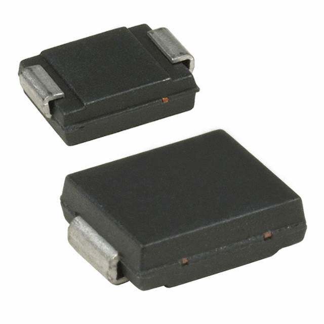
| 产品图片 |
|
| rohs | 符合RoHS不受无铅要求限制 / 符合限制有害物质指令(RoHS)规范要求 |
| 产品系列 | 二极管与整流器,TVS二极管,TVS 二极管 - 瞬态电压抑制器,Littelfuse 1.5KE150A1.5KE |
| 数据手册 | |
| 产品型号 | 1.5KE150A |
| 不同频率时的电容 | - |
| 产品培训模块 | http://www.digikey.cn/PTM/IndividualPTM.page?site=cn&lang=zhs&ptm=22970 |
| 产品目录绘图 |
|
| 产品目录页面 | |
| 产品种类 | TVS 二极管 - 瞬态电压抑制器 |
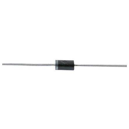
| 供应商器件封装 | DO-201 |
| 其它名称 | 1.5KE150ALFCT |
| 击穿电压 | 143 V |
| 功率-峰值脉冲 | 1500W (1.5kW) |
| 包装 | 剪切带 (CT) |
| 单向通道 | 1 |
| 双向通道 | - |
| 商标 | Littelfuse |
| 安装类型 | 通孔 |
| 安装风格 | Through Hole |
| 封装 | Reel |
| 封装/外壳 | DO-201AA,DO-27,轴向 |
| 封装/箱体 | DO-201 |
| 尺寸 | 5.3 mm Dia. x 9.5 mm L |
| 峰值浪涌电流 | 7.3 A |
| 峰值脉冲功率耗散 | 1.5 kW |
| 工作温度 | -55°C ~ 150°C (TJ) |
| 工作电压 | 128 V |
| 工厂包装数量 | 1200 |
| 应用 | 通用 |
| 最大工作温度 | + 175 C |
| 最小工作温度 | - 55 C |
| 极性 | Unidirectional |
| 标准包装 | 1 |
| 电压-击穿(最小值) | 143V |
| 电压-反向关态(典型值) | 128V |
| 电压-箝位(最大值)@Ipp | 207V |
| 电流-峰值脉冲(10/1000µs) | 7.3A |
| 电源线路保护 | 无 |
| 端接类型 | Axial |
| 类型 | 齐纳 |
| 系列 | 1.5KE |
| 钳位电压 | 207 V |


- 商务部:美国ITC正式对集成电路等产品启动337调查
- 曝三星4nm工艺存在良率问题 高通将骁龙8 Gen1或转产台积电
- 太阳诱电将投资9.5亿元在常州建新厂生产MLCC 预计2023年完工
- 英特尔发布欧洲新工厂建设计划 深化IDM 2.0 战略
- 台积电先进制程称霸业界 有大客户加持明年业绩稳了
- 达到5530亿美元!SIA预计今年全球半导体销售额将创下新高
- 英特尔拟将自动驾驶子公司Mobileye上市 估值或超500亿美元
- 三星加码芯片和SET,合并消费电子和移动部门,撤换高东真等 CEO
- 三星电子宣布重大人事变动 还合并消费电子和移动部门
- 海关总署:前11个月进口集成电路产品价值2.52万亿元 增长14.8%


PDF Datasheet 数据手册内容提取
1N6267A Series (cid:2) 1500 Watt Mosorb Zener Transient Voltage Suppressors Unidirectional* http://onsemi.com Mosorb devices are designed to protect voltage sensitive components from high voltage, high−energy transients. They have Cathode Anode excellent clamping capability, high surge capability, low zener impedance and fast response time. These devices are ON Semiconductor’s exclusive, cost-effective, highly reliable Surmetic(cid:2) axial leaded package and are ideally-suited for use in communication systems, numerical controls, process controls, medical equipment, business machines, power supplies and many AXIAL LEAD other industrial/consumer applications, to protect CMOS, MOS and CASE 41A Bipolar integrated circuits. PLASTIC Features MARKING DIAGRAM • Working Peak Reverse Voltage Range − 5.8 V to 214 V • Peak Power − 1500 Watts @ 1 ms A 1.5KE • ESD Rating of Class 3 (>16 kV) per Human Body Model xxxA 1N6 • Maximum Clamp Voltage @ Peak Pulse Current xxxA YYWW(cid:3) • Low Leakage < 5 (cid:2)A Above 10 V (cid:3) • UL 497B for Isolated Loop Circuit Protection A = Assembly Location • Response Time is Typically < 1 ns 1.5KExxxA = ON Device Code • 1N6xxxA = JEDEC Device Code Pb−Free Packages are Available YY = Year WW = Work Week Mechanical Characteristics = (See Table on Page 3) CASE: Void-free, transfer-molded, thermosetting plastic (cid:3) = Pb−Free Package (Note: Microdot may be in either location) FINISH: All external surfaces are corrosion resistant and leads are readily solderable ORDERING INFORMATION MAXIMUM LEAD TEMPERATURE FOR SOLDERING PURPOSES: 230°C, 1/16 in from the case for 10 seconds Device Package Shipping† POLARITY: Cathode indicated by polarity band 1.5KExxxA Axial Lead 500 Units/Box MOUNTING POSITION: Any 1.5KExxxAG Axial Lead 500 Units/Box (Pb−Free) 1.5KExxxARL4 Axial Lead 1500/Tape & Reel 1.5KExxxARL4G Axial Lead 1500/Tape & Reel (Pb−Free) 1N6xxxA Axial Lead 500 Units/Box 1N6xxxAG Axial Lead 500 Units/Box (Pb−Free) 1N6xxxARL4 Axial Lead 1500/Tape & Reel 1N6xxxARL4G Axial Lead 1500/Tape & Reel (Pb−Free) †For information on tape and reel specifications, including part orientation and tape sizes, please refer to our Tape and Reel Packaging Specifications *For additional information on our Pb−Free strategy and soldering details, please Brochure, BRD8011/D. download the ON Semiconductor Soldering and Mounting Techniques Preferred devices are recommended choices for future use Reference Manual, SOLDERRM/D. and best overall value. © Semiconductor Components Industries, LLC, 2005 1 Publication Order Number: July, 2005 − Rev. 7 1N6267A/D
1N6267A Series MAXIMUM RATINGS Rating Symbol Value Unit Peak Power Dissipation (Note 1) @ TL ≤ 25°C PPK 1500 W Steady State Power Dissipation PD 5.0 W @ TL ≤ 75°C, Lead Length = 3/8 in Derated above TL = 75°C 20 mW/°C Thermal Resistance, Junction−to−Lead R(cid:3)JL 20 °C/W Forward Surge Current (Note 2) @ TA = 25°C IFSM 200 A Operating and Storage TJ, Tstg −65 to +175 °C Temperature Range Maximum ratings are those values beyond which device damage can occur. Maximum ratings applied to the device are individual stress limit values (not normal operating conditions) and are not valid simultaneously. If these limits are exceeded, device functional operation is not implied, damage may occur and reliability may be affected. 1. Nonrepetitive current pulse per Figure 5 and derated above TA = 25°C per Figure 2. 2. 1/2 sine wave (or equivalent square wave), PW = 8.3 ms, duty cycle = 4 pulses per minute maximum. NOTES: Please see 1.5KE6.8CA to 1.5KE250CA for Bidirectional Devices ELECTRICAL CHARACTERISTICS (TA = 25°C unless otherwise noted, VF = 3.5 V Max., IF (Note 3) = 100 A) I Symbol Parameter IF IPP Maximum Reverse Peak Pulse Current VC Clamping Voltage @ IPP VRWM Working Peak Reverse Voltage IR Maximum Reverse Leakage Current @ VRWM VCVBRVRWM V IR VF VBR Breakdown Voltage @ IT IT IT Test Current (cid:4)VBR Maximum Temperature Coefficient of VBR IF Forward Current IPP VF Forward Voltage @ IF Uni−Directional TVS http://onsemi.com 2
1N6267A Series ELECTRICAL CHARACTERISTICS (TA = 25°C unless otherwise noted, VF = 3.5 V Max. @ IF (Note 3) = 100 A) Breakdown Voltage VC @ IPP (Note 7) JEDEC VRWM Device† (Note 5) IR @ VRWM VBR (Note 6) (Volts) @ IT VC IPP (cid:2)VBR Device† (Note 4) (Volts) ((cid:2)A) Min Nom Max (mA) (Volts) (A) (%/°C) 1.5KE6.8A, G 1N6267A, G 5.8 1000 6.45 6.8 7.14 10 10.5 143 0.057 1.5KE7.5A, G 1N6268A, G 6.4 500 7.13 7.5 7.88 10 11.3 132 0.061 1.5KE8.2A, G 1N6269A, G 7.02 200 7.79 8.2 8.61 10 12.1 124 0.065 1.5KE9.1A, G 1N6270A, G 7.78 50 8.65 9.1 9.55 1 13.4 112 0.068 1.5KE10A, G 1N6271A, G 8.55 10 9.5 10 10.5 1 14.5 103 0.073 1.5KE11A, G 1N6272A, G 9.4 5 10.5 11 11.6 1 15.6 96 0.075 1.5KE12A, G 1N6273A, G 10.2 5 11.4 12 12.6 1 16.7 90 0.078 1.5KE13A, G 1N6274A, G 11.1 5 12.4 13 13.7 1 18.2 82 0.081 1.5KE15A, G 1N6275A, G 12.8 5 14.3 15 15.8 1 21.2 71 0.084 1.5KE16A, G 1N6276A, G 13.6 5 15.2 16 16.8 1 22.5 67 0.086 1.5KE18A, G 1N6277A, G 15.3 5 17.1 18 18.9 1 25.2 59.5 0.088 1.5KE20A, G 1N6278A, G 17.1 5 19 20 21 1 27.7 54 0.09 1.5KE22A, G 1N6279A, G 18.8 5 20.9 22 23.1 1 30.6 49 0.092 1.5KE24A, G 1N6280A, G 20.5 5 22.8 24 25.2 1 33.2 45 0.094 1.5KE27A, G 1N6281A, G 23.1 5 25.7 27 28.4 1 37.5 40 0.096 1.5KE30A, G 1N6282A, G 25.6 5 28.5 30 31.5 1 41.4 36 0.097 1.5KE33A, G 1N6283A, G 28.2 5 31.4 33 34.7 1 45.7 33 0.098 1.5KE36A, G 1N6284A, G 30.8 5 34.2 36 37.8 1 49.9 30 0.099 1.5KE39A, G 1N6285A, G 33.3 5 37.1 39 41 1 53.9 28 0.1 1.5KE43A, G 1N6286A, G 36.8 5 40.9 43 45.2 1 59.3 25.3 0.101 1.5KE47A, G 1N6287A, G 40.2 5 44.7 47 49.4 1 64.8 23.2 0.101 1.5KE51A, G 1N6288A, G 43.6 5 48.5 51 53.6 1 70.1 21.4 0.102 1.5KE56A, G 1N6289A, G 47.8 5 53.2 56 58.8 1 77 19.5 0.103 1.5KE62A, G 1N6290A, G 53 5 58.9 62 65.1 1 85 17.7 0.104 1.5KE68A, G 1N6291A, G 58.1 5 64.6 68 71.4 1 92 16.3 0.104 1.5KE75A, G 1N6292A, G 64.1 5 71.3 75 78.8 1 103 14.6 0.105 1.5KE82A, G 1N6293A, G 70.1 5 77.9 82 86.1 1 113 13.3 0.105 1.5KE91A, G 1N6294A, G 77.8 5 86.5 91 95.5 1 125 12 0.106 1.5KE100A, G 1N6295A, G 85.5 5 95 100 105 1 137 11 0.106 1.5KE110A, G 1N6296A, G 94 5 105 110 116 1 152 9.9 0.107 1.5KE120A, G 1N6297A, G 102 5 114 120 126 1 165 9.1 0.107 1.5KE130A, G 1N6298A, G 111 5 124 130 137 1 179 8.4 0.107 1.5KE150A, G 1N6299A, G 128 5 143 150 158 1 207 7.2 0.108 1.5KE160A, G 1N6300A, G 136 5 152 160 168 1 219 6.8 0.108 1.5KE170A, G 1N6301A, G 145 5 162 170 179 1 234 6.4 0.108 1.5KE180A, G 1N6302A, G* 154 5 171 180 189 1 246 6.1 0.108 1.5KE200A, G 1N6303A, G 171 5 190 200 210 1 274 5.5 0.108 1.5KE220A, G 185 5 209 220 231 1 328 4.6 0.109 1.5KE250A, G 214 5 237 250 263 1 344 5 0.109 Devices listed in bold, italic are ON Semiconductor Preferred devices. Preferred devices are recommended choices for future use and best overall value. 3. 1/2 sine wave (or equivalent square wave), PW = 8.3 ms, duty cycle = 4 pulses per minute maximum. 4. Indicates JEDEC registered data 5. A transient suppressor is normally selected according to the maximum working peak reverse voltage (VRWM), which should be equal to or greater than the dc or continuous peak operating voltage level. 6. VBR measured at pulse test current IT at an ambient temperature of 25°C 7. Surge current waveform per Figure 5 and derate per Figures 1 and 2. †The “G” suffix indicates Pb−Free package available. *Not Available in the 1500/Tape & Reel http://onsemi.com 3
1N6267A Series 100 NONREPETITIVE C PULSE WAVEFORM F25° SHOWN IN FIGURE 5 % OT= A POWER (kW) 10 DERATING IN CURRENT @ 10800 PEAK ULSE R OR 60 P, PK AK POWE 40 EP PK A 20 E P 1 0 0.1(cid:2)(cid:2)s 1(cid:2)(cid:2)s 10(cid:2)(cid:2)s 100(cid:2)(cid:2)s 1 ms 10 ms 0 25 50 75 100 125 150 175 200 tP, PULSE WIDTH TA, AMBIENT TEMPERATURE (°C) Figure 1. Pulse Rating Curve Figure 2. Pulse Derating Curve 1N6373, ICTE-5, MPTE-5, 1N6267A/1.5KE6.8A through through 1N6389, ICTE-45,C, MPTE-45,C 1N6303A/1.5KE200A 10,000 10,000 MEASURED @ ZERO BIAS MEASURED @ ZERO BIAS 1000 1000 F) F) p p E ( MEASURED @ VRWM E ( C C N N A A MEASURED @ V T T RWM ACI 100 ACI 100 P P A A C C C, C, 10 10 1 10 100 1000 1 10 100 1000 VBR, BREAKDOWN VOLTAGE (VOLTS) VBR, BREAKDOWN VOLTAGE (VOLTS) Figure 3. Capacitance versus Breakdown Voltage S) T T A W PULSE WIDTH (t ) IS DEFINED AS TION ( 3/8″ tr TCHUARTR PEONTIN DT EWCHAPEYRSE T OTH 5E0 %PE OAFK IPP. SSIPA 5 3/8″ %) 100 PEAK VALUE − IPP tr ≤ 10(cid:2)(cid:2)s OWER DI 4 VALUE ( HALF VALUE − IPP E P 3 , PP 50 2 T I A T S 2 Y D t EA 1 P T S , D 0 0 P 0 25 50 75 100 125 150 175 200 0 1 2 3 4 TL, LEAD TEMPERATURE (°C) t, TIME (ms) Figure 4. Steady State Power Derating Figure 5. Pulse Waveform http://onsemi.com 4
1N6267A Series 1N6373, ICTE-5, MPTE-5, 1.5KE6.8CA through through 1N6389, ICTE-45,C, MPTE-45,C 1.5KE200CA 1000 V (cid:2)=(cid:2)6.8 to 13(cid:2)V 1000 V (cid:2)=(cid:2)6.8 to 13(cid:2)V T (cid:2)=(cid:2)25°C BR(NOM) T (cid:2)=(cid:2)25°C BR(NOM) 500 tL(cid:2)=(cid:2)10(cid:2)(cid:2)s 20(cid:2)V 500 tL(cid:2)=(cid:2)10(cid:2)(cid:2)s 20(cid:2)V P 24(cid:2)V 43(cid:2)V P 24(cid:2)V 43(cid:2)V S) 200 S) 200 75(cid:2)V P P AM 100 AM 100 T ( T ( N 50 N 50 E E R R R R CU 20 CU 20 180(cid:2)V ST 10 ST 10 120(cid:2)V E E , T 5 , T 5 T T I I 2 2 1 1 0.3 0.5 0.7 1 2 3 5 7 10 20 30 0.3 0.5 0.7 1 2 3 5 7 10 20 30 (cid:5)V , INSTANTANEOUS INCREASE IN V ABOVE V (VOLTS) (cid:5)V , INSTANTANEOUS INCREASE IN V ABOVE V (VOLTS) BR BR BR(NOM) BR BR BR(NOM) Figure 6. Dynamic Impedance 1 0.7 0.5 0.3 R 0.2 O PULSE WIDTH T C 10 ms FA 0.1 G N 0.07 ATI 0.05 R 1 ms E D 0.03 0.02 100 (cid:2)s 10 (cid:2)s 0.01 0.1 0.2 0.5 1 2 5 10 20 50 100 D, DUTY CYCLE (%) Figure 7. Typical Derating Factor for Duty Cycle APPLICATION NOTES RESPONSE TIME application, since the main purpose for adding a transient In most applications, the transient suppressor device is suppressor is to clamp voltage spikes. These devices have placed in parallel with the equipment or component to be excellent response time, typically in the picosecond range protected. In this situation, there is a time delay associated and negligible inductance. However, external inductive with the capacitance of the device and an overshoot effects could produce unacceptable overshoot. Proper condition associated with the inductance of the device and circuit layout, minimum lead lengths and placing the the inductance of the connection method. The capacitance suppressor device as close as possible to the equipment or effect is of minor importance in the parallel protection components to be protected will minimize this overshoot. scheme because it only produces a time delay in the Some input impedance represented by Zin is essential to transition from the operating voltage to the clamp voltage as prevent overstress of the protection device. This impedance shown in Figure 8. should be as high as possible, without restricting the circuit The inductive effects in the device are due to actual operation. turn-on time (time required for the device to go from zero DUTY CYCLE DERATING current to full current) and lead inductance. This inductive The data of Figure 1 applies for non-repetitive conditions effect produces an overshoot in the voltage across the and at a lead temperature of 25°C. If the duty cycle increases, equipment or component being protected as shown in the peak power must be reduced as indicated by the curves Figure 9. Minimizing this overshoot is very important in the of Figure 7. Average power must be derated as the lead or http://onsemi.com 5
1N6267A Series ambient temperature rises above 25°C. The average power the 10 (cid:2)s pulse. However, when the derating factor for a derating curve normally given on data sheets may be given pulse of Figure 7 is multiplied by the peak power value normalized and used for this purpose. of Figure 1 for the same pulse, the results follow the At first glance the derating curves of Figure 7 appear to be expected trend. in error as the 10 ms pulse has a higher derating factor than TYPICAL PROTECTION CIRCUIT Z in V LOAD V in L V (TRANSIENT) in OVERSHOOT DUE TO V V (TRANSIENT) V INDUCTIVE EFFECTS in V L V L V in t d t = TIME DELAY DUE TO CAPACITIVE EFFECT D t t Figure 8. Figure 9. UL RECOGNITION* The entire series has Underwriters Laboratory Conditioning, Temperature test, Dielectric Voltage- Recognition for the classification of protectors (QVGV2) Withstand test, Discharge test and several more. under the UL standard for safety 497B and File #116110. Whereas, some competitors have only passed a Many competitors only have one or two devices recognized flammability test for the package material, we have been or have recognition in a non-protective category. Some recognized for much more to be included in their Protector competitors have no recognition at all. With the UL497B category. recognition, our parts successfully passed several tests including Strike Voltage Breakdown test, Endurance *Applies to 1.5KE6.8A, CA thru 1.5KE250A, CA CLIPPER BIDIRECTIONAL DEVICES 1. Clipper-bidirectional devices are available in the 3. The 1N6267A through 1N6303A series are JEDEC 1.5KEXXA series and are designated with a “CA” registered devices and the registration does not include suffix; for example, 1.5KE18CA. Contact your nearest a “CA” suffix. To order clipper-bidirectional devices ON Semiconductor representative. one must add CA to the 1.5KE device title. 2. Clipper-bidirectional part numbers are tested in both directions to electrical parameters in preceding table (except for V which does not apply). F http://onsemi.com 6
1N6267A Series OUTLINE DIMENSIONS MOSORB CASE 41A−04 ISSUE D B NOTES: 1. DIMENSIONING AND TOLERANCING PER ANSI D Y14.5M, 1982. 2. CONTROLLING DIMENSION: INCH. 3. LEAD FINISH AND DIAMETER UNCONTROLLED IN DIMENSION P. 4. 041A−01 THRU 041A−03 OBSOLETE, NEW STANDARD 041A−04. K P INCHES MILLIMETERS DIM MIN MAX MIN MAX A 0.335 0.374 8.50 9.50 P B 0.189 0.209 4.80 5.30 A D 0.038 0.042 0.96 1.06 K 1.000 −−− 25.40 −−− P −−− 0.050 −−− 1.27 K http://onsemi.com 7
1N6267A Series Mosorb and Surmetic are trademarks of Semiconductor Components Industries, LLC. ON Semiconductor and are registered trademarks of Semiconductor Components Industries, LLC (SCILLC). SCILLC reserves the right to make changes without further notice to any products herein. SCILLC makes no warranty, representation or guarantee regarding the suitability of its products for any particular purpose, nor does SCILLC assume any liability arising out of the application or use of any product or circuit, and specifically disclaims any and all liability, including without limitation special, consequential or incidental damages. “Typical” parameters which may be provided in SCILLC data sheets and/or specifications can and do vary in different applications and actual performance may vary over time. All operating parameters, including “Typicals” must be validated for each customer application by customer’s technical experts. SCILLC does not convey any license under its patent rights nor the rights of others. SCILLC products are not designed, intended, or authorized for use as components in systems intended for surgical implant into the body, or other applications intended to support or sustain life, or for any other application in which the failure of the SCILLC product could create a situation where personal injury or death may occur. Should Buyer purchase or use SCILLC products for any such unintended or unauthorized application, Buyer shall indemnify and hold SCILLC and its officers, employees, subsidiaries, affiliates, and distributors harmless against all claims, costs, damages, and expenses, and reasonable attorney fees arising out of, directly or indirectly, any claim of personal injury or death associated with such unintended or unauthorized use, even if such claim alleges that SCILLC was negligent regarding the design or manufacture of the part. SCILLC is an Equal Opportunity/Affirmative Action Employer. This literature is subject to all applicable copyright laws and is not for resale in any manner. PUBLICATION ORDERING INFORMATION LITERATURE FULFILLMENT: N. American Technical Support: 800−282−9855 Toll Free ON Semiconductor Website: http://onsemi.com Literature Distribution Center for ON Semiconductor USA/Canada P.O. Box 61312, Phoenix, Arizona 85082−1312 USA Order Literature: http://www.onsemi.com/litorder Phone: 480−829−7710 or 800−344−3860 Toll Free USA/Canada Japan: ON Semiconductor, Japan Customer Focus Center Fax: 480−829−7709 or 800−344−3867 Toll Free USA/Canada 2−9−1 Kamimeguro, Meguro−ku, Tokyo, Japan 153−0051 For additional information, please contact your Email: orderlit@onsemi.com Phone: 81−3−5773−3850 local Sales Representative. http://onsemi.com 1N6267A/D 8
Mouser Electronics Authorized Distributor Click to View Pricing, Inventory, Delivery & Lifecycle Information: O N Semiconductor: 1.5KE100ARL4 1.5KE100ARL4G 1.5KE10A 1.5KE10AG 1.5KE10ARL4 1.5KE10ARL4G 1.5KE110ARL4 1.5KE110ARL4G 1.5KE11A 1.5KE11AG 1.5KE11ARL4 1.5KE11ARL4G 1.5KE120ARL4 1.5KE120ARL4G 1.5KE12A 1.5KE12AG 1.5KE12ARL4 1.5KE12ARL4G 1.5KE130A 1.5KE130AG 1.5KE130ARL4 1.5KE130ARL4G 1.5KE13ARL4 1.5KE13ARL4G 1.5KE150A 1.5KE150AG 1.5KE150ARL4 1.5KE150ARL4G 1.5KE15A 1.5KE15AG 1.5KE15ARL4 1.5KE15ARL4G 1.5KE160ARL4 1.5KE160ARL4G 1.5KE16A 1.5KE16AG 1.5KE16ARL4 1.5KE16ARL4G 1.5KE170ARL4 1.5KE170ARL4G 1.5KE180A 1.5KE180AG 1.5KE180ARL4 1.5KE180ARL4G 1.5KE18A 1.5KE18AG 1.5KE18ARL4 1.5KE18ARL4G 1.5KE200A 1.5KE200AG 1.5KE200ARL4 1.5KE200ARL4G 1.5KE20A 1.5KE20AG 1.5KE20ARL4 1.5KE20ARL4G 1.5KE220ARL4 1.5KE220ARL4G 1.5KE22A 1.5KE22AG 1.5KE22ARL4 1.5KE22ARL4G 1.5KE24A 1.5KE24AG 1.5KE24ARL4 1.5KE24ARL4G 1.5KE250A 1.5KE250AG 1.5KE250ARL4 1.5KE250ARL4G 1.5KE27A 1.5KE27AG 1.5KE27ARL4 1.5KE27ARL4G 1.5KE30A 1.5KE30AG 1.5KE30ARL4 1.5KE30ARL4G 1.5KE33A 1.5KE33AG 1.5KE33ARL4 1.5KE33ARL4G 1.5KE36A 1.5KE36AG 1.5KE36ARL4 1.5KE36ARL4G 1.5KE39ARL4 1.5KE39ARL4G 1.5KE43A 1.5KE43AG 1.5KE43ARL4 1.5KE43ARL4G 1.5KE47A 1.5KE47AG 1.5KE47ARL4 1.5KE47ARL4G 1.5KE51ARL4 1.5KE51ARL4G 1.5KE56A 1.5KE56AG